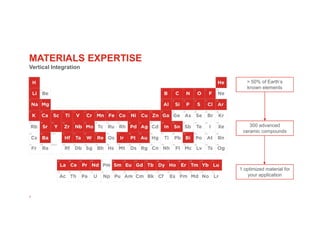
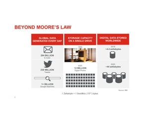
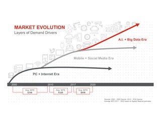
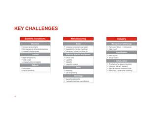
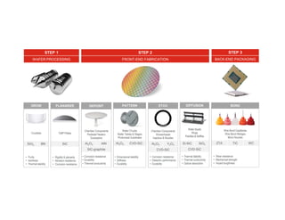
Dean Warner
02 May 2018
Image: TESCAN
Ceramic Solutions enabling the
Evolution of Semiconductor
Processing
2
ENGINEERED CERAMICS
Technology leader
61/118
5000
CoorsTek
61 / 118
Applying over half the known elements
VISION
We make the world measurably better
EXPERTISE
5000 ceramics-focused employees
Technology Roadshow
3
MATERIALS EXPERTISE
Vertical Integration
> 50% of Earth’s
known elements
300 advanced
ceramic compounds
1 optimized material for
your application
4
“Age of Si” limited by:
• Heat (thermodynamics)
• Leakage (quantum mechanics)
Remains effective “Coordination device”
BEYOND MOORE’S LAW
“Moore’s Law is more what you’d
call a ‘guideline’ than actual rule”
Image: Intel
5
GLOBAL DATA
GENERATED EVERY DAY
294 BILLION
E-mails
230 MILLION
Tweets
1+ BILLION
Google Searches
STORAGE CAPACITY
ON A SINGLE DRIVE
1956:
2 Digital Photos
2020:
12 MILLION
Digital Photos
Source: IBM
1 Zettabyte = 1 Sextillion (1021) bytes
BEYOND MOORE’S LAW
DIGITAL DATA STORED
WORLDWIDE
2018:
~4.4 zettabytes
2020:
~44 zettabytes
6
A.I. + Big Data Era
Mobile + Social Media Era
PC + Internet Era
MARKET EVOLUTION
Avg. WFE
$25B
Avg. WFE
$32B
Avg. WFE
$45B
Sources: 2000 – 2009 Gartner. 2010 – 2016 Gartner.
Average WFE 2017 – 2020 based on Applied Material estimates.
2000 2010 2017 2020
Layers of Demand Drivers
7
“Internet of Things” (IoT)
EXPLOSION OF DATA GENERATION
A city of 1M people will generate 200M GB of data per day by 2020
Source: Applied Materials model based on forecasts
published by Cisco, Intel, Western Digital.
SMART BUILDINGS
55M
GB/day
SMART FACTORIES
50M
GB/day
PUBLIC SAFETY
SYSTEMS
50M
GB/day
SOCIAL MEDIA +
OTHER
2M
GB/day
SMART VEHICLES
40M
GB/day
SMART AIRPLANES
4M
GB/day
8
• 3D - NAND (5x ≥ x 96, 128)
• String stacking (3D - NAND)
• Multiple Patterning DRAM
(1x, 1y, 1z)
• High Aspect Ratio DRAM
• Next-Gen Memory (Cross-
point, ReRam, MRam)
MEMORY PROCESSES
• ALE
• ALD
• EUV Lithography
• Advanced EPI
CITIUS, ALTIUS, FORTIUS
LAM Research
Applied
Materials
Too Many Options?
LOGIC
• Bulk FinFET (≤10 nm, N20/N7)
• SOI FinFET (N7/N5)
• <10 nm Line Width
• Gate-All-Around
(GAA)/Nanowire)
• GAAFETS (≤ 5 nm), (X)FETs
9
DRAM
Logic
Source: Lam Research
NAND
>mid 2x
20 nm/
1x nm
<1y nm
Gen 5+
Gen 4
Gen 3
3D NAND
Gen 1/2/3
2D NAND
<10 nm
14/16 nm
>20 nm
2017 20202017 2020 2017 2020
DRAM NAND
Increasing WFE Intensity to Support BIT
Supply Growth
WFE Needed to Achieve 1% BIT Supply Growth
Storage (Memory)
Node ReductionNext-Gen Architecture
CITIUS, ALTIUS, FORTIUS
Increasing Process Complexity and Intensity
10
Affordability
&
Sustainability
Process
Complexity
Output Density Product Cost Sustainability
• Wafer size
• Wafer yield, full
usage
Surface
Integrity
Selectivity Damage Killer Defects
Metal
Contamination • Particle generation
• Purity
• Robustness
Considerations
Atomic-Scale
Precision
High Aspect
Ratio Structures
Feature-Scale
Uniformity
Wafer-Scale
Uniformity
Repeatability
• Enabling processes
- ALD, ALE, EUV
• Chamber matching
CITIUS, ALTIUS, FORTIUS
Source: Lam Research
11
Extreme Conditions Manufacturing Industry
Chemical
Thermal
Defects
Scale
Ceramic-
Specific
Equipment
CollaborationSkills
Metrology
Specification
Management of
Change
Key Challenges
WHAT CERAMICS BRING TO THE PARTY
12
KEY CHALLENGES
Extreme Conditions
Chemical
• Corrosive environments
• More aggressive etchants/atmospheres
• Increased chamber power
Thermal
• Higher temperatures
• Faster cycles
• Increased uniformity/stability
Defects
• Particulation
• Impurity sensitivity
Manufacturing
Scale
• Increasing component size (wafer)
• Repeatability (chamber matching)
• Tolerances - inches to achieve nm
Ceramic-Specific Equipment
• Critical mass
• Capability
• Reliability
• Integrated systems
Skills
• Machining
• Lean Engineering
Metrology
• Capability/detectability
• Practicality (real-time, cost effective)
Industry
Management of Change
• High cost of failure → risk aversion
• Copy Exact!
Specification
• Make-to-print
• Ship-to-control
Collaboration
• IP protection (eg plasma chemistry)
• Edisonian “fail fast” approach
• Rapid & intensive investment cycle
• Resources – iterate while sustaining
13
WHAT CERAMICS BRING TO THE PARTY
Materials
Critical Properties
Chemical
• Purity
• Corrosion/Plasma resistance
Mechanical
• Erosion/abrasion resistance
• Strength
• Stiffness
• Polishability
Thermal
• Stability
• Uniformity
• Shock resistance
Electrical
• Resistivity
• Dielectrics
• Electrostatic discharging
Optical
• Absorption
Processing
Key Factors
Microstructure/Phase Control
• Purity
• Corrosion/Plasma resistance
Dimensional
• Shape complexity
• Size
• Tolerancing
• Features
Surface Properties
• Surface finish
• Integrity
Repeatabilty
• Stack-ups
• Chamber matching
Materials
• Purity
• Targeted functionality/performance
Manufacturing
• Process control
• Equipment size
• In-situ metrology
• DFM
• Modelling
• Progressive training
Industry
Major Trends
14
DIFFUSION
Wafer Boats
Rings
Paddles & Baffles
Si-SiC SiO2
CVD-SiC
• Thermal stability
• Thermal conductivity
• Optical absorption
ETCH
Chamber Components
Showerheads
Injectors & Nozzles
Al2O3 Y2O3
CVD-SiC
• Corrosion resistance
• Dielectric performance
• Durability
PATTERN
Wafer Chucks
Wafer Tables & Stages
Photomask Substrates
Al2O3 CVD-SiC
• Dimensional stability
• Stiffness
• Durability
DEPOSIT
Chamber Components
Pedestal Heaters
Susceptors
Al2O3 AlN
SiC-graphite
• Corrosion resistance
• Durability
• Thermal conductivity
BOND
Wire Bond Capillaries
Wire Bond Wedges
Micro Nozzles
ZTA TiC WC
• Wear resistance
• Mechanical strength
• Impact toughness
PLANARIZE
CMP Plates
SiC
• Rigidity & planarity
• Abrasion resistance
• Corrosion resistance
GROW
Crucibles
SiO2 BN
• Purity
• Inertness
• Thermal stability
STEP 1
WAFER PROCESSING
STEP 2
FRONT-END FABRICATION
STEP 3
BACK-END PACKAGING
Questions?
Come visit us in
booth #200
16 CoorsTek Confidential
The average IC design cost for a 16nm/14nm chip is $80 million,
compared to $30 million for a 28nm planar device, according to
Gartner. It costs $271 million to design a 7nm chip, according to
Gartner.
Intel is America’s largest high-technology capital expenditure investor
($5.1 billion in the U.S. 2015) and its third largest investor in global
R&D ($12.1 billion in 20151).
Chipmakers want EUV for 7nm and/or 5nm
Others agree. “7nm will be a big node,” said Rick Gottscho,
executive vice president and chief technology officer at Lam
Research. “The industry cadence seems to be that every other
node is bigger.
Samsung will invest $7 billion over a three-year period to ramp
up a Chinese fab to expand production of NAND flash memory
that’s in strong demand for smartphones and other mobile
devices. 08-17
At $99.6 billion, the DRAM market is forecast to be by
far the largest single product category in the IC industry
in 2018, exceeding the expected NAND flash market
($62.1 billion) by $37.5 billion. (IC Industry)
The '22nm,' '32nm' etc. number you refer to is the device half-
pitch. This number is half of the distance between a feature on
one transistor and an identical feature on the next transistor
over.
17 CoorsTek Confidential
3D NAND will continue to be a big driver for equipment in 2018. In 3D
NAND alone, Samsung’s capital spending outlays will reach a
staggering $14 billion in 2017, according to IC Insights. In total,
Samsung’s capital outlays are $26 billion in 2017, including 3D NAND,
DRAM ($7 billion) and foundry ($5 billion). (SemiEngineering)
In 2017, memory has been the big driver for fab equipment.
2018 is expected to follow a similar pattern. “The tremendous
demand for memory technology has produced record shipment
levels,” Applied’s Sherman said. “DRAM and NAND content in
smartphones continues to grow. The average NAND content in
smartphones has been growing by roughly 50% recently, going
from approximately 24 gigabytes in 2016 to approximately 38
gigabytes today. (SemiEngineering)
SSDs also are driving demand for NAND.
Besides the conversion rate, there are questions about how far 3D NAND
will scale. In 2017, 3D NAND suppliers have been migrating from 48 layer
to 64 layer devices with 96 layer products in R&D. “We will see 96 layer
devices (in 2018),” Lam’s Gottscho said. “The new generation will double
the density every year.”
The development of a 96-layer NAND device is challenging, however.
Today’s etch tools and hard masks could run out of steam for this
technology. As a result, the industry is migrating towards a manufacturing
technique called string stacking. For this, vendors will develop two 48-
layer 3D NAND devices and connect them, thereby forming a 96-layer 3D
device. “So we’ll have two-tier 3D NAND—48 plus 48 layers. That will be
done out of necessity,” Gottscho said.
With string stacking, 3D NAND could scale up to 512 or more layers.
String stacking, however, adds more manufacturing costs to the equation,
presenting some new and difficult challenges for the industry
German engineering company Bosch has placed a
big bet on the future value of the IoT, with a €1 billion
investment to build a wafer fabrication centre in
Dresden, Germany. 06-17
3D NAND will lead product sector spending, growing 3
percent each in 2018 and 2019, to US$16 billion and
US$17 billion, respectively. DRAM will see robust growth
of 26 percent in 2018, to US$14 billion, but is expected to
decline 14 percent to US$12 billion in 2019. Foundries will
increase equipment spending by 2 percent to US$17
billion in 2018 and by 26 percent to US$22 billion in 2019,
primarily to support 7nm investments and ramp of new
capacity (Semi 03/18)
18
19

Ceramic Solutions Enabling the Evolution of Semiconductor Processing

  • 1.
    Dean Warner 02 May2018 Image: TESCAN Ceramic Solutions enabling the Evolution of Semiconductor Processing
  • 2.
    2 ENGINEERED CERAMICS Technology leader 61/118 5000 CoorsTek 61/ 118 Applying over half the known elements VISION We make the world measurably better EXPERTISE 5000 ceramics-focused employees Technology Roadshow
  • 3.
    3 MATERIALS EXPERTISE Vertical Integration >50% of Earth’s known elements 300 advanced ceramic compounds 1 optimized material for your application
  • 4.
    4 “Age of Si”limited by: • Heat (thermodynamics) • Leakage (quantum mechanics) Remains effective “Coordination device” BEYOND MOORE’S LAW “Moore’s Law is more what you’d call a ‘guideline’ than actual rule” Image: Intel
  • 5.
    5 GLOBAL DATA GENERATED EVERYDAY 294 BILLION E-mails 230 MILLION Tweets 1+ BILLION Google Searches STORAGE CAPACITY ON A SINGLE DRIVE 1956: 2 Digital Photos 2020: 12 MILLION Digital Photos Source: IBM 1 Zettabyte = 1 Sextillion (1021) bytes BEYOND MOORE’S LAW DIGITAL DATA STORED WORLDWIDE 2018: ~4.4 zettabytes 2020: ~44 zettabytes
  • 6.
    6 A.I. + BigData Era Mobile + Social Media Era PC + Internet Era MARKET EVOLUTION Avg. WFE $25B Avg. WFE $32B Avg. WFE $45B Sources: 2000 – 2009 Gartner. 2010 – 2016 Gartner. Average WFE 2017 – 2020 based on Applied Material estimates. 2000 2010 2017 2020 Layers of Demand Drivers
  • 7.
    7 “Internet of Things”(IoT) EXPLOSION OF DATA GENERATION A city of 1M people will generate 200M GB of data per day by 2020 Source: Applied Materials model based on forecasts published by Cisco, Intel, Western Digital. SMART BUILDINGS 55M GB/day SMART FACTORIES 50M GB/day PUBLIC SAFETY SYSTEMS 50M GB/day SOCIAL MEDIA + OTHER 2M GB/day SMART VEHICLES 40M GB/day SMART AIRPLANES 4M GB/day
  • 8.
    8 • 3D -NAND (5x ≥ x 96, 128) • String stacking (3D - NAND) • Multiple Patterning DRAM (1x, 1y, 1z) • High Aspect Ratio DRAM • Next-Gen Memory (Cross- point, ReRam, MRam) MEMORY PROCESSES • ALE • ALD • EUV Lithography • Advanced EPI CITIUS, ALTIUS, FORTIUS LAM Research Applied Materials Too Many Options? LOGIC • Bulk FinFET (≤10 nm, N20/N7) • SOI FinFET (N7/N5) • <10 nm Line Width • Gate-All-Around (GAA)/Nanowire) • GAAFETS (≤ 5 nm), (X)FETs
  • 9.
    9 DRAM Logic Source: Lam Research NAND >mid2x 20 nm/ 1x nm <1y nm Gen 5+ Gen 4 Gen 3 3D NAND Gen 1/2/3 2D NAND <10 nm 14/16 nm >20 nm 2017 20202017 2020 2017 2020 DRAM NAND Increasing WFE Intensity to Support BIT Supply Growth WFE Needed to Achieve 1% BIT Supply Growth Storage (Memory) Node ReductionNext-Gen Architecture CITIUS, ALTIUS, FORTIUS Increasing Process Complexity and Intensity
  • 10.
    10 Affordability & Sustainability Process Complexity Output Density ProductCost Sustainability • Wafer size • Wafer yield, full usage Surface Integrity Selectivity Damage Killer Defects Metal Contamination • Particle generation • Purity • Robustness Considerations Atomic-Scale Precision High Aspect Ratio Structures Feature-Scale Uniformity Wafer-Scale Uniformity Repeatability • Enabling processes - ALD, ALE, EUV • Chamber matching CITIUS, ALTIUS, FORTIUS Source: Lam Research
  • 11.
    11 Extreme Conditions ManufacturingIndustry Chemical Thermal Defects Scale Ceramic- Specific Equipment CollaborationSkills Metrology Specification Management of Change Key Challenges WHAT CERAMICS BRING TO THE PARTY
  • 12.
    12 KEY CHALLENGES Extreme Conditions Chemical •Corrosive environments • More aggressive etchants/atmospheres • Increased chamber power Thermal • Higher temperatures • Faster cycles • Increased uniformity/stability Defects • Particulation • Impurity sensitivity Manufacturing Scale • Increasing component size (wafer) • Repeatability (chamber matching) • Tolerances - inches to achieve nm Ceramic-Specific Equipment • Critical mass • Capability • Reliability • Integrated systems Skills • Machining • Lean Engineering Metrology • Capability/detectability • Practicality (real-time, cost effective) Industry Management of Change • High cost of failure → risk aversion • Copy Exact! Specification • Make-to-print • Ship-to-control Collaboration • IP protection (eg plasma chemistry) • Edisonian “fail fast” approach • Rapid & intensive investment cycle • Resources – iterate while sustaining
  • 13.
    13 WHAT CERAMICS BRINGTO THE PARTY Materials Critical Properties Chemical • Purity • Corrosion/Plasma resistance Mechanical • Erosion/abrasion resistance • Strength • Stiffness • Polishability Thermal • Stability • Uniformity • Shock resistance Electrical • Resistivity • Dielectrics • Electrostatic discharging Optical • Absorption Processing Key Factors Microstructure/Phase Control • Purity • Corrosion/Plasma resistance Dimensional • Shape complexity • Size • Tolerancing • Features Surface Properties • Surface finish • Integrity Repeatabilty • Stack-ups • Chamber matching Materials • Purity • Targeted functionality/performance Manufacturing • Process control • Equipment size • In-situ metrology • DFM • Modelling • Progressive training Industry Major Trends
  • 14.
    14 DIFFUSION Wafer Boats Rings Paddles &Baffles Si-SiC SiO2 CVD-SiC • Thermal stability • Thermal conductivity • Optical absorption ETCH Chamber Components Showerheads Injectors & Nozzles Al2O3 Y2O3 CVD-SiC • Corrosion resistance • Dielectric performance • Durability PATTERN Wafer Chucks Wafer Tables & Stages Photomask Substrates Al2O3 CVD-SiC • Dimensional stability • Stiffness • Durability DEPOSIT Chamber Components Pedestal Heaters Susceptors Al2O3 AlN SiC-graphite • Corrosion resistance • Durability • Thermal conductivity BOND Wire Bond Capillaries Wire Bond Wedges Micro Nozzles ZTA TiC WC • Wear resistance • Mechanical strength • Impact toughness PLANARIZE CMP Plates SiC • Rigidity & planarity • Abrasion resistance • Corrosion resistance GROW Crucibles SiO2 BN • Purity • Inertness • Thermal stability STEP 1 WAFER PROCESSING STEP 2 FRONT-END FABRICATION STEP 3 BACK-END PACKAGING
  • 15.
  • 16.
    16 CoorsTek Confidential Theaverage IC design cost for a 16nm/14nm chip is $80 million, compared to $30 million for a 28nm planar device, according to Gartner. It costs $271 million to design a 7nm chip, according to Gartner. Intel is America’s largest high-technology capital expenditure investor ($5.1 billion in the U.S. 2015) and its third largest investor in global R&D ($12.1 billion in 20151). Chipmakers want EUV for 7nm and/or 5nm Others agree. “7nm will be a big node,” said Rick Gottscho, executive vice president and chief technology officer at Lam Research. “The industry cadence seems to be that every other node is bigger. Samsung will invest $7 billion over a three-year period to ramp up a Chinese fab to expand production of NAND flash memory that’s in strong demand for smartphones and other mobile devices. 08-17 At $99.6 billion, the DRAM market is forecast to be by far the largest single product category in the IC industry in 2018, exceeding the expected NAND flash market ($62.1 billion) by $37.5 billion. (IC Industry) The '22nm,' '32nm' etc. number you refer to is the device half- pitch. This number is half of the distance between a feature on one transistor and an identical feature on the next transistor over.
  • 17.
    17 CoorsTek Confidential 3DNAND will continue to be a big driver for equipment in 2018. In 3D NAND alone, Samsung’s capital spending outlays will reach a staggering $14 billion in 2017, according to IC Insights. In total, Samsung’s capital outlays are $26 billion in 2017, including 3D NAND, DRAM ($7 billion) and foundry ($5 billion). (SemiEngineering) In 2017, memory has been the big driver for fab equipment. 2018 is expected to follow a similar pattern. “The tremendous demand for memory technology has produced record shipment levels,” Applied’s Sherman said. “DRAM and NAND content in smartphones continues to grow. The average NAND content in smartphones has been growing by roughly 50% recently, going from approximately 24 gigabytes in 2016 to approximately 38 gigabytes today. (SemiEngineering) SSDs also are driving demand for NAND. Besides the conversion rate, there are questions about how far 3D NAND will scale. In 2017, 3D NAND suppliers have been migrating from 48 layer to 64 layer devices with 96 layer products in R&D. “We will see 96 layer devices (in 2018),” Lam’s Gottscho said. “The new generation will double the density every year.” The development of a 96-layer NAND device is challenging, however. Today’s etch tools and hard masks could run out of steam for this technology. As a result, the industry is migrating towards a manufacturing technique called string stacking. For this, vendors will develop two 48- layer 3D NAND devices and connect them, thereby forming a 96-layer 3D device. “So we’ll have two-tier 3D NAND—48 plus 48 layers. That will be done out of necessity,” Gottscho said. With string stacking, 3D NAND could scale up to 512 or more layers. String stacking, however, adds more manufacturing costs to the equation, presenting some new and difficult challenges for the industry German engineering company Bosch has placed a big bet on the future value of the IoT, with a €1 billion investment to build a wafer fabrication centre in Dresden, Germany. 06-17 3D NAND will lead product sector spending, growing 3 percent each in 2018 and 2019, to US$16 billion and US$17 billion, respectively. DRAM will see robust growth of 26 percent in 2018, to US$14 billion, but is expected to decline 14 percent to US$12 billion in 2019. Foundries will increase equipment spending by 2 percent to US$17 billion in 2018 and by 26 percent to US$22 billion in 2019, primarily to support 7nm investments and ramp of new capacity (Semi 03/18)
  • 18.
  • 19.