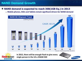
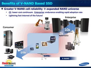
The document discusses Samsung's new 3D V-NAND flash memory technology.
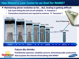
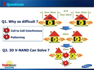
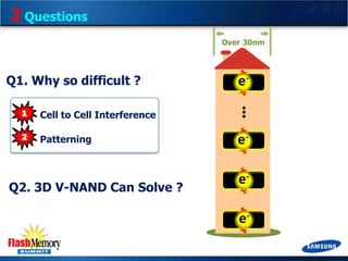
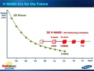
[1] Planar NAND scaling limitations meant that continued density increases required prohibitively expensive manufacturing processes and posed reliability risks, threatening the ability to satisfy future demands for high-capacity, low-cost storage.
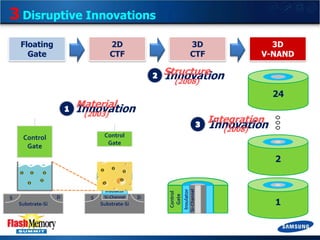
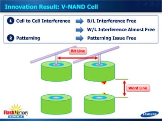
[2] Samsung's new 3D V-NAND technology solves these issues by stacking multiple layers of memory cells vertically. This novel 3D structure eliminates cell interference issues and removes patterning limitations of planar NAND.
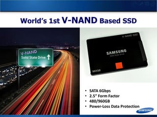
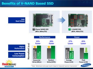
[3] Samsung has launched the first V-NAND-based SSDs, which offer significant benefits like higher performance, lower power consumption, and reduced manufacturing costs compared to planar


![SSD Market Forecast
SSD market growth has always been constrained
• Doubts about keeping up $/Gb improvements
• Concerns about degrading NAND Flash parameters
Planar NAND
(Endurance, Performance, Retention..)
Endurance
Performance
$/Gb
[Samsung Projection based on 2013 2Q iSuppli market forecast ]](https://image.slidesharecdn.com/20130813keynotebelliotjung-131014180752-phpapp01/85/Samsung-presents-Ushering-in-the-3D-Memory-Era-with-V-NAND-at-Flash-Memory-Summit-2013-26-320.jpg)
![SSD Market Forecast
SSD market growth has always been constrained
• Doubts about keeping up $/Gb improvements
• Concerns about degrading NAND Flash parameters
Planar NAND
(Endurance, Performance, Retention..)
Endurance
Performance
$/Gb
K Units
Enterprise
K Units
[Samsung Projection based on 2013 2Q iSuppli market forecast ]
Client](https://image.slidesharecdn.com/20130813keynotebelliotjung-131014180752-phpapp01/85/Samsung-presents-Ushering-in-the-3D-Memory-Era-with-V-NAND-at-Flash-Memory-Summit-2013-27-320.jpg)
![SSD Market Forecast with V-NAND Impact
V-NAND
“SSD for Everyone!”
K Units
Enterprise
K Units
Client
2X
3X
[Samsung Projection based on 2013 2Q iSuppli market forecast ]](https://image.slidesharecdn.com/20130813keynotebelliotjung-131014180752-phpapp01/85/Samsung-presents-Ushering-in-the-3D-Memory-Era-with-V-NAND-at-Flash-Memory-Summit-2013-28-320.jpg)