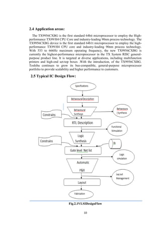
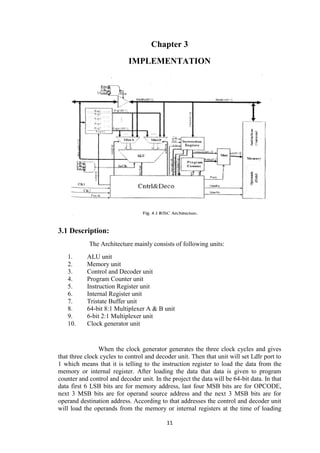
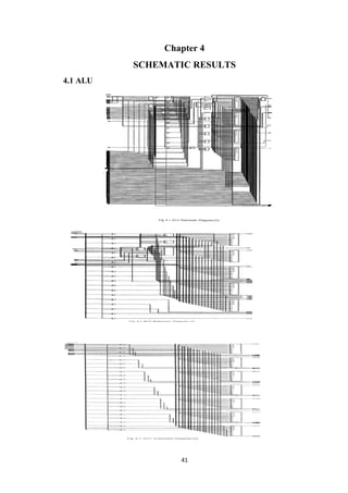
This document discusses the design of a 64-bit RISC processor IP core. It was submitted as a project report by four students for their Bachelor of Technology degree. The report covers the implementation of various blocks of the RISC processor like the ALU, memory, control unit, program counter, registers, etc. using Verilog HDL. It provides algorithms, code snippets, waveform diagrams to explain the design and functioning of each block. The overall goal of the project was to design a 64-bit RISC processor IP core that can execute basic instructions involving arithmetic, logical and data transfer operations within a single clock cycle for applications that require fast instruction execution.
![14
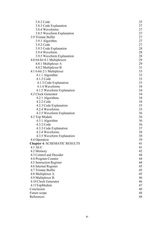
17. If SelC is 1101 it is allocated to skip operation
18. If SelC is 1110 it is allocated to jump operation
19. If SelC is 1111 it is allocated to halt operation
20. If SelC is default pass OutA to AluOut
21. Stop
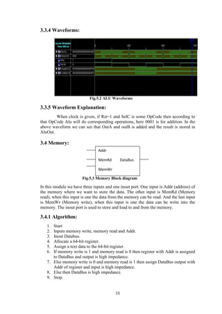
3.3.2 Code:
„timescale 1ns/1ps
module alu_1 (OutA, OutB, Rst, SelC, InClk, AluOut);
input Rst, InClk;
input [3:0] SelC;
input [63:0] OutA, OutB;
output reg [63:0] AluOut;
always @ (negedge InClk)
Begin
If (Rst == 1'b1)
Case (SelC)
//4'b0000:AluOut=default;
4'b0001: AluOut=OutA+OutB;
4'b0010: AluOut=OutA-OutB;
4'b0011: AluOut=OutA*OutB;
4'b0100: AluOut=OutA+1'b1;
4'b0101: AluOut=OutA-1'b1;
4'b0110: AluOut=OutA&OutB;
4'b0111: AluOut=OutA| OutB;
4'b1000: AluOut=OutA^OutB;
4'b1001: AluOut=OutA<<1;
4'b1010: AluOut=OutA>>1;
4'b1011: AluOut=OutA;
4'b1100: AluOut=~OutA;
endcase
end
endmodule
3.3.3 Code explanation:
As mention above ALU module collects two input data, one is OpCode and
one InClk and a reset. When InClk go to negative edge and Rst indicate low; then a
case statement is written as SelC (OpCode) as selection. This choice is given to a
specific OpCode (operation needs to perform) using the two input data‟s.
We left four choices for DEFALT, JMP, SKIP and HALT operations. We
assigned 0000 OpCode for DEFALT, 1101 is for SKIP, 1110 for JMP and 1111 for
HALT.](https://image.slidesharecdn.com/1a9d8d2d-4e61-4036-b742-5804091f8619-150213201742-conversion-gate01/85/cd-2-Batch-id-33-22-320.jpg)
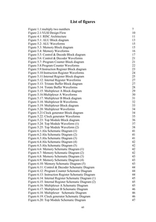
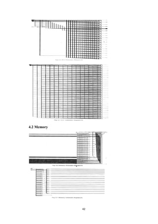
![16
3.4.2 Code
„timescale 1ns/1ps
module memory_1 (DataBus, MemWr, MemRd, Addr);
inout [63:0] DataBus;
input MemWr;
input MemRd;
input [5:0] Addr;
reg [63:0] datareg;
reg [63:0] Mem [0:63];
//initial $fread ("om.bin", Mem);
initial $readmemh ("om.txt", Mem);
always @ (MemWr or MemRd or Addr or datareg)
begin
if (MemWr==1'b1 && MemRd==1'b0)
begin
Mem [Addr] =DataBus;
datareg=64'hzzzzzzzzzzzzzzzz;
end
else if (MemWr==1'b0 && MemRd==1'b1)
datareg= Mem [Addr];
else
datareg=64'hzzzzzzzzzzzzzzzz;
end
assign DataBus = datareg;
endmodule
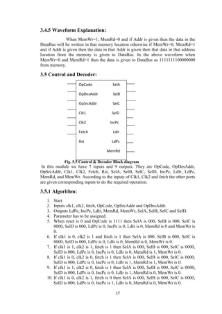
3.4.3 Code Explanation:
When the inputs MemWr==1’b1 and MemRd==1’b0 the data which is in the
DataBus is loaded into the memory the specified address and if the inputs MemWr==1’b0
and MemRd==1’b1 the data from the memory is loaded into the datareg(internal register)
after that it is loaded into the DataBus.
3.4.4 Waveforms:
Fig. 5.4 Memory waveforms](https://image.slidesharecdn.com/1a9d8d2d-4e61-4036-b742-5804091f8619-150213201742-conversion-gate01/85/cd-2-Batch-id-33-24-320.jpg)
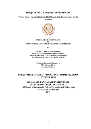
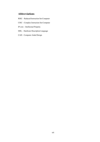
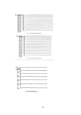
![18
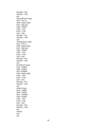
11. If clk1 is 1, clk2 is 1, fetch is 0 then SelA is 111, SelB is 000, SelC is 0000,
SelD is 000, LdPc is 0, IncPc is 0, LdIr is 0, MemRd is 1, MemWr is 0.
12. If clk 1 is 0, clk2 is 0, fetch is 0 then SelA is 111, SelB is 000, SelC is 0000,
SelD is 000, LdPc is 0, IncPc is 0, LdIr is 0, MemRd is 1, and MemWr is 0.
13. If clk1 is 1, clk2 is 0, fetch is 0 then SelA is 000, SelB is 000, SelC is 0000,
SelD is 000, LdPc is 0, IncPc is 0, LdIr is 0, MemRd is 0, and MemWr is 0.
14. Default is SelA is 000, SelB is 000, SelC is 0000, SelD is 000, LdPc is o,
IncPc is 0, LdIr is 0, MemRd is 0, and MemWr is 0.
15. Stop.
3.5.2 Code:
„timescale 1ns/1ps
module
controler1(Clk1,Clk2,Fetch,Rst,OpCode,OpSrcAddr,OpDesAddr,LdIr,Ldpc,Incpc,Me
mRd,MemWr, SelA, SelB b, SelC, SelD);
input Clk1, Clk2, Fetch, Rst; input [3:0] OpCode; input [2:0] OpSrcAddr,
OpDesAddr;
output reg LdIr, LdPc, IncPc, MemRd, MemWr;
output reg [2:0] SelA, SelB, SelD;
output reg [3:0] SelC;
parameter AddrSetUp1 =3'b011;
parameter InstrFetch =3'b111;
parameter InstrLoad =3'b001;
parameter Idle =3'b101;
parameter AddrSetUp2 =3'b010;
parameter OperandFetch =3'b110;
parameter AluOperation =3'b000;
parameter StoreResult =3'b100;
wire [2:0] Control;
assign Control={Clk1,Clk2,Fetch};
always @ (Control or Rst or OpCode or OpSrcAddr or OpDesAddr)
begin
if(Rst==1'b0 && OpCode==4'b1111)
begin
SelA =3'b000;
SelB =3'b000;
SelC =4'b0000;
SelD =3'b000;
LdPc =1'b0;
IncPc=1'b0;
LdIr =1'b0;
MemRd =1'b0;
MemWr =1'b0;
end
else
begin
case (Control)
AddrSetUp1: begin
SelA =3'b000;](https://image.slidesharecdn.com/1a9d8d2d-4e61-4036-b742-5804091f8619-150213201742-conversion-gate01/85/cd-2-Batch-id-33-26-320.jpg)

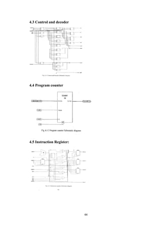
![22
4. If positive edge of IncPc and negative edge of Rst.
5. Then if reset is 0 then PcOut is 0.
6. Else LdPc is 1 then PcOut is Mem Addr.
7. Else IncPc by one.
8. Stop.
3.6.2 Code:
„timescale 1ns/1ps
module pro_count (MemAddr, IncPc, LdPc, Rst, Pcout);
input [5:0] MemAddr; input IncPc, LdPc, Rst;
output [5:0] Pcout; reg [5:0] sreg;
assign Pcout = sreg [5:0];
always @(posedge IncPc or negedge Rst)
begin
if (Rst == 1'b0)
sreg = 6'b000000;
else if (LdPc == 1'b1)
begin
sreg = MemAddr;
end
else
sreg = sreg + 1;
end endmodule
3.6.3 Code Explanation:
If Rst is 0 then sreg (internal register) is set to 0 and if Rst is 1 and if LdPc
(Load program counter) is 1 then memory address is loaded into the sreg and if LdPc
is 0 then sreg is incremented.
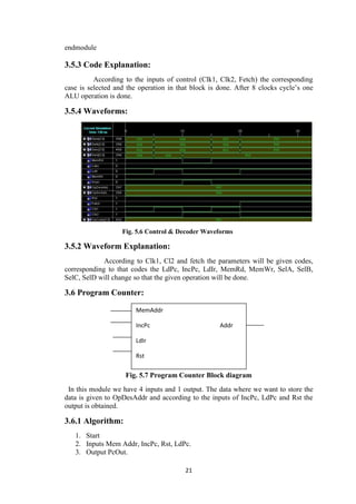
3.6.4 Waveforms:
Fig. 5.8 Program Counter Waveforms
3.6.5 Waveform Explanation:
When Rst is 1 is given (here is a Clk) if LdPc is 1 then the MemAddr is
given to Pcout else if LdPc is 0 then the MemAddr is incremented. In the above](https://image.slidesharecdn.com/1a9d8d2d-4e61-4036-b742-5804091f8619-150213201742-conversion-gate01/85/cd-2-Batch-id-33-30-320.jpg)
![23
waveform when LdPc is 1, 11 from MemAddr is loaded into PcOut else if it is
incremented to 12, etc.
3.7 Instruction Register:
Fig.5.9 Instruction Register Block diagram
In this module we have 4 inputs and 4 outputs. According to the inputs of LdIr
(instruction register) and Clk the data from the DataBus is loaded into dreg (internal
register) or incremented. And if Reset is 0 then the data in the dreg is 0. The required
number of bits is given to the corresponding output ports like OpCode, OpDesAddr,
OpSrcAddr and MemAddr.
3.7.1 Algorithm:
1. Start.
2. Inputs Clk, Rst, LdIr, DataBus.
3. Output OpCode, OpDesAddr, OpSrcAddr, MemAddr.
4. Parameters OpCode is DataBus (63-60), OpSrcAddr is DataBus (59-57),
OpDesAddr (56-54) and MemAddr is DataBus (5-0) has to be assigned.
5. If Clk is positive edge and Rst is negative edge then if Rst is 0 then Databus is
zero.
6. Else if LdIr is 1 then DataBus is DataBus and if OpCode is 1101 then
increment MemAddr by one.
7. Else DataBus is DataBus.
8. Stop.
3.7.2 Code:
timescale 1ns/1ps
module m1 (DataBus, Clk, LdIr, Rst, OpCode, OpSrcAddr, OpDesAddr, MemAddr);
input Clk;
input Rst;
input LdIr;
input [63:0] DataBus;
output [5:0] OpCode;
output [5:0] OpSrcAddr;;
output [5:0] OpDesAddr;
output [5:0] MemAddr;
reg [5:0] sreg;
assign OpCode=dreg [63:60];
assign OpSrcAddr=dreg [59:57];
assign OpDesAddr=dreg [56:54];
assign MemAddr=dreg [5:0];
always @ (posedge Clk or negedge Rst)
DataBus MemAddr
Clk OpCode
LdIr
OpSrcAddr
Rst
OpDesAddr](https://image.slidesharecdn.com/1a9d8d2d-4e61-4036-b742-5804091f8619-150213201742-conversion-gate01/85/cd-2-Batch-id-33-31-320.jpg)
![24
begin
if (Rst==1'b0)
dreg=64'h0000000000000000;
else if (LdIr==1'b1)
begin
dreg=DataBus;
if (dreg [63:60] =4'b1101)
dreg [5:0] =dreg [5:0] +1;
end
else
dreg=dreg;
end
endmodule
3.7.3 Code Explanation:
If Rst is 0 then dreg is 0. And if Rst is 1 and if LdIr is 1 then DataBus is
loaded into dreg or else dreg is unchanged. The last 4 bits (63:60) of DataBus is given
to OpCode, the 3 bits (59:57) is given to OpSrcAddr, the next 3 bits (56:54) are given
to OpDesAddr and the first 6 bits are given to (5:0) is given to MemAddr.
3.7.4 Waveforms:
Fig. 5.10 Instruction Register Waveforms
3.7.5 Waveform Explanation:
When Clk and Rst are given and if LdIr is 1 then the DataBus is given to
OpCode, OpSrcAddr, OpDesAddr and MemAddr to their bit length. In the above
waveform if LdIr is 1 then OpCode= B, OpSrcAddr=0, OpDesAddr=5 and
MemAddr=00.](https://image.slidesharecdn.com/1a9d8d2d-4e61-4036-b742-5804091f8619-150213201742-conversion-gate01/85/cd-2-Batch-id-33-32-320.jpg)
![25
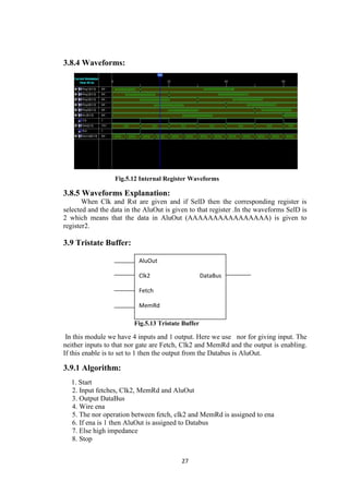
3.8 Internal Registers:
Fig.5.11 Internal Register Block diagram
In this module we have 4 inputs and 6 outputs. Based on the input of SelD the output
of Alu (AluOut) is loaded into the dreg (internal register). And if reset is 0 then all the
registers are set to zero.
3.8.1 Algorithm:
1. Start
2. Input Clk, Rst, SelD, AluOut.
3. Output Reg1, Reg2, Reg3, Reg4, Reg5, Acc
4. Assign data registers to registers
5. If Clk is positive edge is negative edge then if reset is zero then Reg1=0, Reg2=0,
Reg3=0, Reg4=0, Reg5=0 and Acc=0
6. Else if Rst=1 and is SelD is 001then reg1=AluOut, if SelD is 010 then
reg2=AluOut, if SelD is 011then reg3=AluOut, if SelD is 100then reg4=AluOut, if
SelD is 101 then reg5=AluOut, if SelD is 110 then reg6=AluOut
7. Else default is reg1=reg1, reg2=reg2, reg3=reg3, reg4=reg4, reg5=reg5, reg6=reg6
8. Stop
3.8.2 Code:
„Timescale 1ns/1ps
module Program _Counter (Clk, Rst, SelD, AluOut, Reg1, Reg2, Reg3, Reg4, Reg5,
Acc);
input Clk;
input Rst;
input [2:0] SelD;
input [63:0] AluOut;
output [63:0] Reg1;
output [63:0] Reg2;
output [63:0] Reg3;
output [63:0] Reg4;
output [63:0] Reg5;
output [5:0] Acc;
reg [5:0] dreg1, dreg2, dreg3, dreg4, dreg5, dreg5;
AluOut Acc
SelD Reg1
Clk Reg2
Rst Reg3
Reg4
Reg5](https://image.slidesharecdn.com/1a9d8d2d-4e61-4036-b742-5804091f8619-150213201742-conversion-gate01/85/cd-2-Batch-id-33-33-320.jpg)
![26
assign Reg1=dreg1;
assign Reg2=dreg2;
assign Reg3=dreg3;
assign Reg4=dreg4;
assign Reg5=dreg5;
assign Acc=dreg6;
always @ (posedge Clk or negedge Rst or SelD)
begin
if (Rst==1'b0)
dreg1=64'h0000000000000000;
dreg2=64'h0000000000000000;
dreg3=64'h0000000000000000;
dreg4=64'h0000000000000000;
dreg5=64'h0000000000000000;
dreg6=64'h0000000000000000;
end
else
case (SelD)
3'b001:dreg1=AluOut;
3'b010:dreg2=AluOut;
3'b011:dreg3=AluOut;
3'b100:dreg4=AluOut;
3'b101:dreg5=AluOut;
3'b110:dreg6=AluOut;
default:
begin dreg1=dreg1;
dreg2=dreg2;
dreg3=dreg3;
dreg4=dreg4;
dreg5=dreg5;
dreg6=dreg6;
end
endcase
end
endmodule
else if (LdIr==1'b1)
begin
dreg=DataBus;
if (dreg [63:60] = 4'b1101)
dreg [5:0] = dreg [5:0] +1;
end
else
dreg=dreg;
end
endmodule
3.8.3 Code Explanation:
If Rst is 0 then all the registers are set to zero or else according to the
input of SelD the AluOut is loaded into the corresponding (based on SelD) register.](https://image.slidesharecdn.com/1a9d8d2d-4e61-4036-b742-5804091f8619-150213201742-conversion-gate01/85/cd-2-Batch-id-33-34-320.jpg)
![28
3.9.2 Code:
„timescale 1ns/1ps
module buffer (fetch, clk2, MemRd, AluOut, Databus)
input fetch;
input clk2;
input MemRd;
wire ena;
input [63:0] AluOut;
output [63:0] Databus;
reg [63:0] Databus;
nor n1 (ena, fetch, clk2, MemRd);
always@ (AluOut or ena)
begin
if (ena==1'b1)
Databus=AluOut;
else
Databus=64'hzzzzzzzzzzzzzzzz;
end
endmodule
3.9.3 Code Explanation:
If the output from the nor gate (enable) is 1 then the data in the AluOut is
loaded into DataBus which means the output and if the enable is 0 then Databus
output is high independence state.
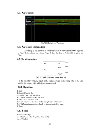
3.9.4 Waveforms:
Fig.5.14 Tristate buffer Waveforms
3.9.5 Waveforms Explanation:
When Clk2, Fetch and MemRd are given then the ena will be either 1 or 0.
If ena is 1 then the data in the AluOut is given to the Databus else Databus is in high
impedance state. In the above example ena=1 then the data in AluOut
(101010101010110) is given to the Databus.](https://image.slidesharecdn.com/1a9d8d2d-4e61-4036-b742-5804091f8619-150213201742-conversion-gate01/85/cd-2-Batch-id-33-36-320.jpg)
![29
4.0 64-bit 8:1 Multiplexers:
4.0.1 Multiplexer A:
Fig.5.15 Multiplexer. A Block diagram
In this module we have 8 inputs and 1 output. The inputs are internal
registers and one select line. Based on the select input corresponding register is
selected and the data which is in loaded into the output port (OutA).
Algorithm:
1. Start
2. Input Databus, reg1, reg2, reg3, reg4, reg5, Acc and SelA.
3. Output OutA.
4. If SelA is 001 OutA is assigned to reg1.
5. Else if SelA is 010 OutA is assigned to reg2.
6. Else if SelA is 011 OutA is assigned to reg3.
7. Else if SelA is 100 OutA is assigned to reg4.
8. Else if SelA is 101 OutA is assigned to reg 5.
9. Else if SelA is 110 OutA is assigned to Acc.
10. Else if SelA is 111 OutA is assigned to Databus.
11. Stop
Code:
module mux_a (Databus, reg1, reg2, reg3, reg4, reg5, acc, SelA, OutA);
input [63:0] Databus;
input [63:0] reg1;
input [63:0] reg2;
input [63:0] reg3;
Acc
Databus
Reg1 OutA
Reg2
Reg3
Reg4
Reg5
Reg6
SelA](https://image.slidesharecdn.com/1a9d8d2d-4e61-4036-b742-5804091f8619-150213201742-conversion-gate01/85/cd-2-Batch-id-33-37-320.jpg)
![30
input [63:0] reg4;
input [63:0] reg5;
input [63:0] acc;
input [2:0] SelA;
output [63:0] OutA;
reg [63:0] OutA;
always @ (SelA or Databus or reg1 or reg2 or reg3 or reg4 or reg5 or acc)
begin
case (SelA)
3'b001: OutA=reg1;
3'b010: OutA=reg2;
3'b011: OutA=reg3;
3'b100: OutA=reg4;
3'b101: OutA=reg5;
3'b110: OutA=acc;
3'b111: OutA=Databus;
default: OutA=64'hzz;
endcase
end
endmodule
Code Explanation:
Based on the select line the corresponding register is selected and the data in
the register is loaded into the output port (out A).And if the selection is not suited to
any one of the case then the output is high impedance state.
Waveforms Explanation:
According to the selection of SelA the dreg in DatabuReg1, Reg2, Reg3,
Reg4, Reg5, Acc is given to OutA. In the above waveforms SelA=1 then the dreg1
(AAAAAAAAAAAAAAAAAA) is given to OutA.
Waveforms:
Fig.5.16 Multiplexer A Waveform
.](https://image.slidesharecdn.com/1a9d8d2d-4e61-4036-b742-5804091f8619-150213201742-conversion-gate01/85/cd-2-Batch-id-33-38-320.jpg)
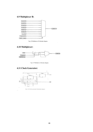
![31
4.0.2 Multiplexer B:
Fig.5.17 Multiplexer B Block diagram
In this module we have 8 inputs and 1 output. The inputs are internal
registers and one select line. Based on the select input corresponding register is
selected and the dat which is in loaded into the output port (OutA).
Algorithm:
1. Start
2. Input Databus reg1, reg2, reg3, reg4, reg5, Acc and SelB.
3. Output outB.
4. If SelB is 001 outB is assigned to reg1.
5. Else if SelB is 010 outB is assigned to reg2.
6. Else if SelB is 011 outB is assigned to reg3.
7. Else if SelB is 100 outB is assigned to reg4.
8. Else if SelB is 101 outB is assigned to reg 5.
9. Else if SelB is 110 OutB is assigned to Acc.
10. Else if SelB is 111 OutB is assigned to Databus.
11. Stop
Code:
module muxb (databus, reg1, reg2, reg3, reg4, reg5, acc, SelA, OutB);
input [63:0] Databus;
input [63:0] reg1;
input [63:0] reg2;
input [63:0] reg3;
input [63:0] reg4;
input [63:0] reg5;
input [63:0] acc;
input [2:0] SelB;
Acc
Databus
Reg1 OutB
Reg2
Reg3
Reg4
Reg5
Reg6
SelB](https://image.slidesharecdn.com/1a9d8d2d-4e61-4036-b742-5804091f8619-150213201742-conversion-gate01/85/cd-2-Batch-id-33-39-320.jpg)
![32
output [63:0] OutB;
reg [63:0] OutB;
always@ (SelB or Databus or reg1 or reg2 or reg3 or reg4 or reg5 or acc)
begin
case (SelB)
3'b001: outB=reg1;
3'b010: outB=reg2;
3'b011: outB=reg3;
3'b100: outB=reg4;
3'b101: outB=reg5;
3'b110: outB=acc;
3'b111: outB=Databus;
default: outB=64'hzz;
endcase
end
endmodule
Code Explanation:
Based on the select line the corresponding register is selected and the data in
the register is loaded into the output port (out B).And if the selection is not suited to
any one of the case then the output is high impedance state.
Waveforms:
Fig.5.17 Multiplexer B Waveforms
Waveforms Explanation:
According to the selection of SelB the data in Databus Reg1, Reg2, Reg3,
Reg4, Reg5, Acc is given to OutB. In the above waveforms SelB=1 then the data in
reg1 (BBBBBBBBBBBBBBBBBB) is given to outB.](https://image.slidesharecdn.com/1a9d8d2d-4e61-4036-b742-5804091f8619-150213201742-conversion-gate01/85/cd-2-Batch-id-33-40-320.jpg)
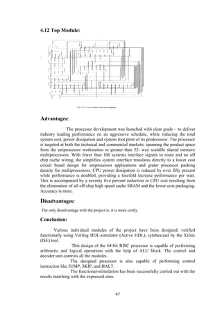
![33
4.1 6-bit 2:1 Multiplexer:
Fig.5.19 Multiplexer Block diagram
In this module we have 3 inputs and 1 output. Based on the input of Fetch output is
depended. The two possible outputs from this module are either MemAddr or PcOut.
4.1.1 Algorithm:
1. Start
2. Inputs MemAddr, PcOut and Fetch
3. Output Addr
If Fetch is 0 then Addr is MemAddr
5. Else Addr is PcOut
6. Stop
4.1.2 Code:
'timescale 1ns/1ps
module mux (MemAddr, PcOut, fetch, Addr);
input [5:0] MemAddr;
input [5:0] Pcout;
input fetch;
output [5:0] Addr;
reg [5:0] Addr;
always@ (fetch or Pcout or MemAddr)
begin
if (fetch==1'b0)
Addr=MemAddr;
else
Addr=PcOut;
end
endmodule
4.1.3 Code Explanation:
If the input Fetch is set to 0 then the output from the port Addr is MemAddr
and if the input Fetch is set to 1 then the output from the port Addr is PcOut.
MemAddr
Addr
Fetch
PcOut](https://image.slidesharecdn.com/1a9d8d2d-4e61-4036-b742-5804091f8619-150213201742-conversion-gate01/85/cd-2-Batch-id-33-41-320.jpg)
![36
4.2.5 Waveforms Explanation:
According to Clk and Rst then ck1, clk2 and fetch are generated. In the
above example when Clk and Rst are 1 then clk1=clk, clk2=1 and fetch is 0.
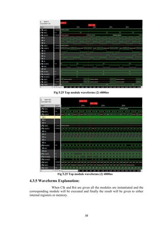
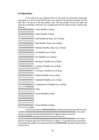
4.3 Top Module:
Fig. 5.23 Top Module Block diagram
In this module only two inputs will be there. The output is data which can be
stored in either memory or internal register. And if we want to take the data from the
memory or internal register data is used as input which means that the data (output) is
used as both input and output. So there is no particular for this module.
4.3.1 Algorithm:
1. Start
2. Inputs Clk, Rst
3. Declare all the inputs and outputs of all individual modules as wires.
4. Create objects for all modules.
5. Stop.
4.3.2 Code:
„Timescale 1ns/1ps
Module topmod_1 (Clk, Rst);
Input Clk, Rst;
Wire Clk1,Clk2,Fetch,Rst,LdIr,Ldpc,Incpc,MemRd,MemWr,InClk;
Wire [2:0] OpSrcAddr, OpDesAddr, SelA, SelB, SelD;
Wire [3:0] OpCode, SelC;
Wire [5:0] MemAddr, Pcout, Addr;
wire [63:0] DataBus,Acc,Reg1,Reg2,Reg3,Reg4,Reg5,AluOut,Data,Outa,Outb;
inst_reg om1 (DataBus, Clk, LdIr, Rst, MemAddr, OpCode, OpDesAddr,
OpSrcAddr);
pro_count om2 (MemAddr, IncPc, LdPc, Rst, Pcout);
mux_2x1 om3 (MemAddr, Pcout, Fetch, Addr);
mux_a om4 (DataBus, Reg1, Reg2, Reg3, Reg4, Reg5, Acc, SelA, OutA);
mux_b om5 (DataBus, Reg1, Reg2, Reg3, Reg4, Reg5, Acc, SelB, OutB);
alu_1 om6 (OutA, OutB, Rst, SelC, InClk, AluOut);
Clk om7 (Clk, Rst, Clk1, Clk2, Fetch);
tri12 om8 (Fetch, Clk2, MemRd, AluOut, DataBus);
memory_1 om9 (DataBus, MemWr, MemRd, Addr);
controller1
om1(Clk1,Clk2,Fetch,Rst,OpCode,OpSrcAddr,OpDesAddr,LdIr,Ldpc,Incpc,MemRd,
MemWr, SelA, SelB, SelC, SelD)
internal_reg_1 om12 (Clk, Rst, SelD, AluOut, Reg1, Reg2, Reg3, Reg4, Reg5, Acc);
Clk
Rst](https://image.slidesharecdn.com/1a9d8d2d-4e61-4036-b742-5804091f8619-150213201742-conversion-gate01/85/cd-2-Batch-id-33-44-320.jpg)


![[Japanese Content] Sumant Mandal_Opportunites in Big Data, The Hive in Japan,...](https://cdn.slidesharecdn.com/ss_thumbnails/sumantmadalopportunitesinbigdataoct29-130920153150-phpapp01-thumbnail.jpg?width=640&height=640&fit=bounds)