Swan(sea) Song – personal research during my six years at Swansea ... and bey...
Ijet12 04-04-020
1. Design and Implementation of I2c master
controller on FPGA using VHDL
Prof. Jai Karan Singh
HOD Electronics and Communication
SSSIST Sehore (MP)-INDIA
Prof. Mukesh Tiwari
Dean Academic
SSSIST Sehore (MP)-INDIA
Vishal Sharma
Dept. of Electronic and Communication
SSSIST Sehore (MP)-INDIA
Abstract - The focus of this paper is on I2C protocol following master controller. This controller is connected to
a microprocessor or computer and reads 8 bit instructions following I2C protocol. The instructions are then
processed and converted to instructions which follow SPI protocol. 32 bit register is designed to send data
serially as per SPI instructions. The complete module is designed in VHDL and simulated in ModelSIM. The
design is also synthesized in Xilinx XST 12.1 and optimized for area and power. This concept is widely
applicable where a microprocessor wants to communicate with SPI device. This module acts as a slave for the
microprocessor at the same time acts like a master for the SPI device which can be considered as a slave. This
design is customized for slowing the data rate according to SPI device, which assures no data loss.
Keywords: – I2C; Handshaking; Master & slave; Serial data transfer ; ISP.
I Introduction
In the world of multiple application based product it is very much a mandatory to have multiple devices
connected to a system, this includes peripherals following different communication protocols as well. This
requirement give rise to the need for an intermediate system which can act as a bridge between 2 devices
following different communication protocols. This is where I2C master controller design is very useful.
Today a system is connected to a number of devices and make the communication smooth and fast, I2C protocol
is considered as one of the very best. But there are number of devices which follow SPI protocol as well. So
such devices can be considered as a slave. The I2C master controller on one end is connected to a PC or
microprocessor, and on the other end it will be connected to the SPI slave. Its main function will be, to
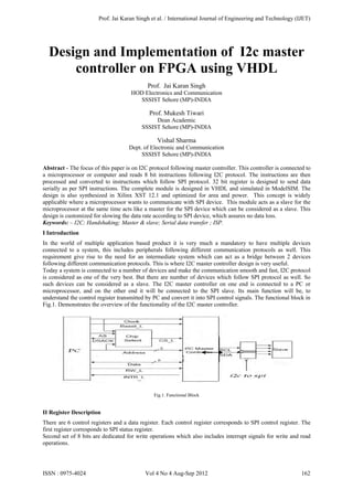
understand the control register transmitted by PC and convert it into SPI control signals. The functional block in
Fig.1. Demonstrates the overview of the functionality of the I2C master controller.
Fig.1. Functional Block
II Register Description
There are 6 control registers and a data register. Each control register corresponds to SPI control register. The
first register corresponds to SPI status register.
Second set of 8 bits are dedicated for write operations which also includes interrupt signals for write and read
operations.
Prof. Jai Karan Singh et al. / International Journal of Engineering and Technology (IJET)
ISSN : 0975-4024 Vol 4 No 4 Aug-Sep 2012 162
2. Third set of 8 bits are dedicated to read operations only 2 bits of this registers are used as bus busy and abort
read signals and rest of the bits are tied to ‘0’.
Fourth and fifth set of 8 bits corresponds to 1st
control register and 2nd
control register of SPI respectively.
Finally sixth set of 8 bits corresponds to baud rate register of SPI.
III Implementation
The PC connected to the controller sends data serially and every 8 bits corresponds a value specified by the i2c
protocol.
The address and the chip select signal selects the I2C device. In this design both chip select and address of the
device are default to 1, as the design is for a specific slave only.
Every set of 8 bits which corresponds to a control registers which controls the flow of data, is stored in registers.
A counter is initialized after successful transmission of 8 bits from the PC to the controller. As the complete set
of control registers are transmitted, all the values of the registers are inverted and stored in a 32 bit register.
32 bit registers are decided on the basis of SPI slave as there are only 4 control register before the data register.
Every bit of the 32 bit register corresponds to a specific signal of SPI protocol.
Once the 32 bit register is fed by the corresponding registers, the serial transmission takes place, which is the
MOSI input of the SPI slave. A clock signal is also transmitted to the SPI slave as SCLK which acts the main
clock for the slave.
IV Results
The following Fig.2. is the simulation results of I2C master controller.
This result shows successful storage of data transmitted by the master on the mentioned address location.
Prof. Jai Karan Singh et al. / International Journal of Engineering and Technology (IJET)
ISSN : 0975-4024 Vol 4 No 4 Aug-Sep 2012 163
3. Fig. 2. Simulation result
Prof. Jai Karan Singh et al. / International Journal of Engineering and Technology (IJET)
ISSN : 0975-4024 Vol 4 No 4 Aug-Sep 2012 164
4. Fig.3. Shows the Technology tree of the I2C master controller
Fig.3. Technology Tree
Prof. Jai Karan Singh et al. / International Journal of Engineering and Technology (IJET)
ISSN : 0975-4024 Vol 4 No 4 Aug-Sep 2012 165
5. Table no1 Shows the Design Summary of the I2C master controller.
Table no 1 . Design Summary
The result shows that minimal resources are utilized in designing the I2C master as only 1 % slices, 1% flip
flops and 1% LUTs are utilized.
V Future Scope & Conclusion
The design of i2c master controller has immense applications in future as the number of devices connected to a
system is only going to increase. So there is always a need for a system which supports multiple protocols. In all
these situations, I2C master controller acts as a great support and will be a key in future design to support
multiple parallel functions. I2C master controller is successfully designed in VHDL and simulated in
ModelSIM. Simulation results verify that the communication has been established between the microprocessor
and the controller. Data processed and the output has been successfully verified as per SPI slave input. The
design meets timing constraints and there are no timing violations. And all these have been achieved with
minimal utilization of resources.
References
[1] A.K. Oudjida, M.L. Berrandjia, R. Tiar, A.Liacha, K. Tahraoui, “FPGA Implementation of I2c & SPI Protocols: A Com-parative
Study” Electronics, Circuits, and Systems, 2009. ICECS 2009
[2] A.K. Oudjida et al, “Master-Slave Wrapper Communication Protocol: A Case Study,” Proceedings of the 1st IEEE International
Computer Systems and Information Tec-hnology Con-ference ICSIT’05, pp 461-467, 19-21 July 2006, Algiers, Algeria.
[3] F. Leens, “An Introduction to I2C and SPI Protocols,” IEEE Instrumentation & Measurement Magazine, pp. 8-13, February
2009.
[4] J.M. Irazabel & S. Blozis, Philips Semiconductors, “I2C-Manual,”Application Note, ref. AN10216-0, March 2003.
[5] M.D. Anu, “I2C to SPI Bridge”, AN49217 Cypress application note, October 2008.
[6] P. Myers, “Interfacing Using Serial Protocoles: Using SPI and I2C”.Available:
http://intranet.daiict.ac.in/~ranjan/esp2005/paper/i2c_spi_341.pdf
[7] Philips Semiconductors, “The IIC-Bus Specifications,” version 2.1, January 2000.
[8] R. Hanabusa, “Comparing JTAG, SPI and I2C,” Spansion’s application note, pp. 1-7, revision 01, April 2007.
Prof. Jai Karan Singh et al. / International Journal of Engineering and Technology (IJET)
ISSN : 0975-4024 Vol 4 No 4 Aug-Sep 2012 166