This document describes a buck converter subsystem and current sensing techniques. It contains the following key points:
1. The objective is to efficiently step down DC voltage while reducing ripple to produce a smooth output voltage, and to measure the inductor current.
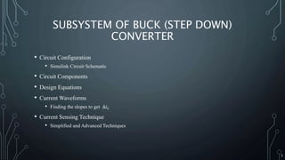
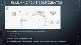
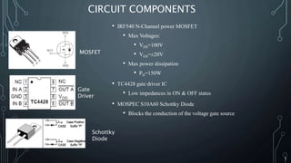
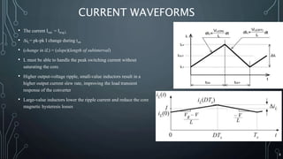
2. The subsystem includes a circuit configuration, components, design equations, and current waveforms. Techniques for current sensing include simplified and advanced methods.
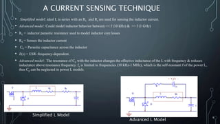
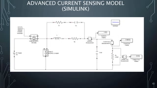
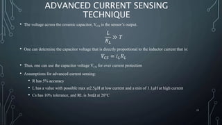
3. An advanced current sensing model uses a simplified inductor model with a parasitic resistance and capacitor to determine the inductor current based on the voltage across a sensing capacitor. Assumptions are provided for component values and tolerances.