Avnet Electronics Marketing, IBM and Endicott Interconnect (EI) are trusted and dependable supply sources
for electronics. US manufacturing facilities and logistics centers provide a highly secure solution, while                         DoMEStIC SuPPlIErS
delivering rapid turnaround on applications. IBM and EI products meet ISO, IPC and military specifications,
RoHS compliance, ITAR registration and are compatible with lead-free assembly processes.

Size, Weight and Power (SWaP) Challenges
Reducing system size, weight, and power (SWaP) is critical to the development of new applications for the
defense aerospace industry. By achieving reductions in the form factor and power consumption of today’s
military electronics, developers are able to improve mobility and extend operational life, enhancing the
overall viability of the product in the marketplace. Avnet Electronics Marketing, IBM and EI have partnered to
help customers leverage System-in-Package (SiP) technology to achieve SWaP goals; bring differentiated
products to market quickly and efficiently and to establish design and supply chain continuity.

Endicott Interconnect
EI is a leading developer of SiP products that integrate multiple IC, assembly and test technologies into modular IC packages. One such product optimized for
aerospace applications is the CoreEZ™. EI’s CoreEZ semiconductor package utilizes the HyperBGA® manufacturing platform to offer a thin core build-up flip chip
package with very dense core vias using a cost sensitive material set. The core via density provides 199 micron via-to-via core pitch resulting in an essentially
coreless structure, which can accommodate ASIC, FPGA and many other semiconductor solutions. EI also offers HyperBGA® packages that are composed of
materials that have passed NASA outgassing testing and are recommended for aerospace applications up to radiation tolerant.

IBM and Avnet
IBM and Avnet work closely together to implement IBM System-on-Chip (SoC) ASIC solutions. IBM’s proven ASIC design systems reduce chip count by combining
FPGAs and older ASICs on single chips. The integration and implementation of qualified sets of tools, libraries, cores and packages enable customers to predictably
design ASICs while closely managing risk. The IBM ASIC design system has been validated through ten generations of ASIC development and more than a thousand
designs, many done in collaboration with Avnet Engineering Services (AES).


           Design & supply Chain expertise                              asiCs anD FounDry                                     Custom paCkaging
          »»Partnerships with IBM and others allow Avnet      »»IBM’s leading-edge technologies,                    »»Proven high-quality, high-reliability and
             to provide ASIC and FPGA solutions from             including Si and SiGe, enable extremely               high-performance ASIC/FPGA packaging
             prototype to production through obsolescence        high-performance, high-density designs
                                                                                                                    »»Turnkey SiP technical solutions
          »»Avnet employs experienced engineers               »» IBM IP portfolio includes
                                                                The
             who expertly staff seven design centers             high-speed serializer and deserializer (HSS)
                                                                                                                    »»Trusted design and packaging capability
             across the United States to maximize                cores, which feature ultra-low jitter generation   »»Substrate & Module Design
             efficiency and provide local support                and enhanced jitter tolerance characteristics          −   Physical design
                                                                 for significant performance advantages
          »»Collaborations with customers have                                                                          −   High-speed, controlled impedance
             yielded more than 2,000 ASIC and FPGA            »»Trusted design and foundry capabilities                 −   Mechanical layout for SiP (MCM)
             designs and have helped Avnet establish                                                                    −   Electrical, mechanical and
             a 100% first time right ASIC design
                                                              »»World-class design, implementation                          thermal modeling
             and implementation track record                     and verification tools plus
                                                                 industry-standard models                           »»Substrate Fabrication
          »» every ASIC and FPGA design
            With                                                                                                        −   50 µm laser-drilled vias
             engagement, customers are able to
                                                              »»Integrated design flow takes ASIC designs
                                                                 from design entry and planning to the                  −   25/25 µm line width & space
             leverage Avnet’s supply chain expertise                                                                    −   Embedded passive
                                                                 silicon implementation of the design
          »»Avnet has serviced the defense aerospace             produced on IBM manufacturing lines                    −   Cu/in/Cu cores
             industry for more than 50+ years and                                                                   »» Assembly
             currently has supply chain solutions in
                                                              »»Established technology provider to the                IC
             place for many key, multi-generational              defense aerospace industry through                     − Flip chip pitch down to 150 µm
             Department of Defense (DoD) programs                MPO and commercial engagements                         − Wirebond, 60 µm inline,
                                                                                                                          43 µm staggered
                                                                                                                        − Flip chip, wirebond, SMD on both sides
IBM ASICs and Foundry
IBM’s leading-edge technologies, including Si and SiGe, enable extremely high-performance, high-density designs. This technology portfolio is complemented by
Avnet Engineering Services’ design engineers and field application engineers (FAEs) who excel at explaining the strengths and challenges associated with myriad
custom logic architectures and are adept at taking customers through a variety of decision-making scenarios to explain the tradeoffs and benefits unique to each.
Together, Avnet and IBM are ready to help customers with diverse needs overcome specific SWaP challenges.


                          SA27E                    Cu11                      Cu08                    Cu65                     Cu45
                      6th Generation           7th Generation            8th Generation           9th Generation          10th Generation
                    ASIC Design System       ASIC Design System        ASIC Design System       ASIC Design System      ASIC Design System


SiP Benefits & SWaP reductions
The push for miniaturization and lightweight, portable computing power has led to breakthroughs in
high-performance electronics packaging by companies such as EI.

  »»
   Organic substrates enable more functionality in            »»
                                                               Reduction in trace length increases
     smaller packages                                             electrical performance

  »»
   Integration of multiple devices into a single package,     »»
                                                               Reduction in signal path length between
     including pre-packaged ICs, surface mount                    die lowers inductance
     components, memory, passives and connectors,
     increases reliability and reduces weight                 »» become less complex or can be
                                                               PCBs
                                                                  eliminated entirely


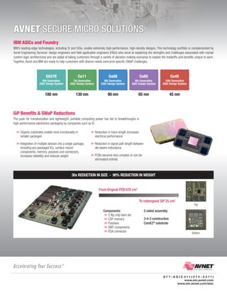
                                              30x rEDuCtIoN IN SIZE - 90% rEDuCtIoN IN WEIGHt


                                                                     From original pCB 670 cm2


                                                                                                     to redesigned sip 25 cm2
                                                                                                                                                 Top
                                                                        Components:                      2-sided assembly
                                                                        »» flip chip bare die
                                                                           5
                                                                        »» memory
                                                                           CSP                           3-4-3 construction
                                                                        »» Passives                      CoreeZ® substrate
                                                                        »» components
                                                                           SMT
                                                                        »» connector
                                                                           PGA                                                                 Bottom


                                                                                                                        8 7 7 - A S I C 4 1 1 ( 2 7 4 - 2 4 1 1 )»
                                                                                                                                        www.em.avnet.com
                                                                                                                                   www.em.avnet.com/asic

Avnet Secure Micro Solutions

  • 1.
    Avnet Electronics Marketing,IBM and Endicott Interconnect (EI) are trusted and dependable supply sources for electronics. US manufacturing facilities and logistics centers provide a highly secure solution, while DoMEStIC SuPPlIErS delivering rapid turnaround on applications. IBM and EI products meet ISO, IPC and military specifications, RoHS compliance, ITAR registration and are compatible with lead-free assembly processes. Size, Weight and Power (SWaP) Challenges Reducing system size, weight, and power (SWaP) is critical to the development of new applications for the defense aerospace industry. By achieving reductions in the form factor and power consumption of today’s military electronics, developers are able to improve mobility and extend operational life, enhancing the overall viability of the product in the marketplace. Avnet Electronics Marketing, IBM and EI have partnered to help customers leverage System-in-Package (SiP) technology to achieve SWaP goals; bring differentiated products to market quickly and efficiently and to establish design and supply chain continuity. Endicott Interconnect EI is a leading developer of SiP products that integrate multiple IC, assembly and test technologies into modular IC packages. One such product optimized for aerospace applications is the CoreEZ™. EI’s CoreEZ semiconductor package utilizes the HyperBGA® manufacturing platform to offer a thin core build-up flip chip package with very dense core vias using a cost sensitive material set. The core via density provides 199 micron via-to-via core pitch resulting in an essentially coreless structure, which can accommodate ASIC, FPGA and many other semiconductor solutions. EI also offers HyperBGA® packages that are composed of materials that have passed NASA outgassing testing and are recommended for aerospace applications up to radiation tolerant. IBM and Avnet IBM and Avnet work closely together to implement IBM System-on-Chip (SoC) ASIC solutions. IBM’s proven ASIC design systems reduce chip count by combining FPGAs and older ASICs on single chips. The integration and implementation of qualified sets of tools, libraries, cores and packages enable customers to predictably design ASICs while closely managing risk. The IBM ASIC design system has been validated through ten generations of ASIC development and more than a thousand designs, many done in collaboration with Avnet Engineering Services (AES). Design & supply Chain expertise asiCs anD FounDry Custom paCkaging »»Partnerships with IBM and others allow Avnet »»IBM’s leading-edge technologies, »»Proven high-quality, high-reliability and to provide ASIC and FPGA solutions from including Si and SiGe, enable extremely high-performance ASIC/FPGA packaging prototype to production through obsolescence high-performance, high-density designs »»Turnkey SiP technical solutions »»Avnet employs experienced engineers »» IBM IP portfolio includes The who expertly staff seven design centers high-speed serializer and deserializer (HSS) »»Trusted design and packaging capability across the United States to maximize cores, which feature ultra-low jitter generation »»Substrate & Module Design efficiency and provide local support and enhanced jitter tolerance characteristics − Physical design for significant performance advantages »»Collaborations with customers have − High-speed, controlled impedance yielded more than 2,000 ASIC and FPGA »»Trusted design and foundry capabilities − Mechanical layout for SiP (MCM) designs and have helped Avnet establish − Electrical, mechanical and a 100% first time right ASIC design »»World-class design, implementation thermal modeling and implementation track record and verification tools plus industry-standard models »»Substrate Fabrication »» every ASIC and FPGA design With − 50 µm laser-drilled vias engagement, customers are able to »»Integrated design flow takes ASIC designs from design entry and planning to the − 25/25 µm line width & space leverage Avnet’s supply chain expertise − Embedded passive silicon implementation of the design »»Avnet has serviced the defense aerospace produced on IBM manufacturing lines − Cu/in/Cu cores industry for more than 50+ years and »» Assembly currently has supply chain solutions in »»Established technology provider to the IC place for many key, multi-generational defense aerospace industry through − Flip chip pitch down to 150 µm Department of Defense (DoD) programs MPO and commercial engagements − Wirebond, 60 µm inline, 43 µm staggered − Flip chip, wirebond, SMD on both sides
  • 2.
    IBM ASICs andFoundry IBM’s leading-edge technologies, including Si and SiGe, enable extremely high-performance, high-density designs. This technology portfolio is complemented by Avnet Engineering Services’ design engineers and field application engineers (FAEs) who excel at explaining the strengths and challenges associated with myriad custom logic architectures and are adept at taking customers through a variety of decision-making scenarios to explain the tradeoffs and benefits unique to each. Together, Avnet and IBM are ready to help customers with diverse needs overcome specific SWaP challenges. SA27E Cu11 Cu08 Cu65 Cu45 6th Generation 7th Generation 8th Generation 9th Generation 10th Generation ASIC Design System ASIC Design System ASIC Design System ASIC Design System ASIC Design System SiP Benefits & SWaP reductions The push for miniaturization and lightweight, portable computing power has led to breakthroughs in high-performance electronics packaging by companies such as EI. »» Organic substrates enable more functionality in »» Reduction in trace length increases smaller packages electrical performance »» Integration of multiple devices into a single package, »» Reduction in signal path length between including pre-packaged ICs, surface mount die lowers inductance components, memory, passives and connectors, increases reliability and reduces weight »» become less complex or can be PCBs eliminated entirely 30x rEDuCtIoN IN SIZE - 90% rEDuCtIoN IN WEIGHt From original pCB 670 cm2 to redesigned sip 25 cm2 Top Components: 2-sided assembly »» flip chip bare die 5 »» memory CSP 3-4-3 construction »» Passives CoreeZ® substrate »» components SMT »» connector PGA Bottom 8 7 7 - A S I C 4 1 1 ( 2 7 4 - 2 4 1 1 )» www.em.avnet.com www.em.avnet.com/asic