AFM.pptx
•Download as PPTX, PDF•
1 like•15 views
This is a physics related presentation that covers the basics , construction , components and working of an atomic force microscope with examples.
Report
Share
Report
Share

Recommended
5. ATOMIC FORCE MICROSCOPE (AFM).pdf
The Atomic Force Microscope (AFM) was invented in 1982 and came to market in 1989. It uses a probe with a very sharp tip to scan over a sample surface, detecting intermolecular forces. As the tip gets closer to the surface and interacts with it, a laser detects deflection in the cantilever probe to create a topographic image map of the surface at nanoscale resolution. The AFM provides 3D imaging of surfaces with accuracy at the nanoscale and can be used in air, liquids, or vacuums to study both living and non-living samples.
nanoscale visualization and characterization.pptx
Scanning probe microscopy (SPM) techniques like atomic force microscopy (AFM) and scanning tunneling microscopy (STM) allow for high-resolution visualization and characterization of materials at the nanoscale. AFM works by scanning a probe with a sharp tip across a sample surface, measuring deflections to create a topography image, while STM uses quantum tunneling of electrons between a tip and conductive surface. These techniques provide sub-nanometer resolution and enable measurement of properties like conductivity, adhesion, and magnetic fields. SPM has advanced understanding of nanoscale phenomena in fields such as electronics, catalysis, and biophysics.
ATOMIC FORCE MICROSCOPE MITHILESH CHOUDHARY
Atomic Force Microscopy is an instrument that gives a complete informatition about topology of specimen.
Afm modified
The document presents a study on characterizing the structure of turtle erythrocyte membranes using atomic force microscopy (AFM). The study isolated turtle erythrocytes, prepared the inner and outer leaflets of the cell membranes, and used AFM imaging and force spectroscopy. Results showed a smooth outer surface with fewer exposed proteins compared to the inner leaflet, which had many proteins covering its surface. Digestion of the inner leaflet with proteinase K removed these proteins. The conclusion is that the inner leaflet of turtle erythrocyte membranes has a large number of proteins, while the outer leaflet has fewer exposed proteins that are mostly glycosylated.
Microscopy
The document discusses different types of microscopy techniques. It describes three main branches of microscopy - optical, electron, and scanning probe microscopy. Optical and electron microscopy use light and electron beams respectively to image samples, while scanning probe microscopy uses a physical probe that interacts with the sample surface. The document then focuses on atomic force microscopy (AFM), providing details on its working principle, modes, image generation process, and applications in measuring surface roughness and thickness. Other scanning probe techniques are also briefly mentioned.
AFM (Atomic Force Microscopy)
Atomic force microscopy (AFM) was developed in 1986 as an extension of scanning tunneling microscopy to image non-conductive surfaces. AFM uses a sharp probe at the end of a flexible cantilever to measure the tiny forces between the probe and sample surface. As the probe scans the surface, these interatomic forces cause the cantilever to deflect, and a laser detects these deflections to create a 3D topographic image of the surface with angstrom-scale resolution. AFM provides topographic and force measurements and can image surfaces in open air or liquid with minimal sample preparation. It has applications in fields including solid state physics, molecular biology, and materials science.
atomicforcemicroscopy-150320212250-conversion-gate01 (1).pptx
The document summarizes atomic force microscopy (AFM). It describes how AFM works by scanning a probe over a sample surface to build a topography map. The key components of an AFM are a microscope stage, control electronics, and computer. AFM uses a piezoelectric transducer to move the tip over the sample while a force transducer senses the force between them. Different scanning modes are contact, non-contact, and tapping mode. AFM provides high resolution imaging at the single atomic level and can be used to image a variety of biological and material science samples.
ETE444-lec2-atomic_scale_characterization_techniques.pdf
The document discusses atomic force microscopy (AFM) and scanning tunneling microscopy (STM) techniques for nanoscale characterization, including a history of their development, operating principles, imaging modes, commercial applications, and examples of AFM tip fabrication methods and molecular imaging. It provides technical details on topics like non-contact versus contact AFM modes, carbon nanotube and other tip materials, and examples of DNA, protein, and nanofabrication imaging.
ETE444-lec2-atomic_scale_characterization_techniques.pdf
The document discusses atomic force microscopy (AFM) and scanning tunneling microscopy (STM) techniques for nanoscale characterization, including a history of their development, operating principles, imaging modes, commercial applications, and examples of AFM tip fabrication methods and molecular imaging. It provides technical details on topics like non-contact dynamic mode AFM, carbon nanotube tips, and single-molecule force recognition events measured with AFM.
Nanolithography
This document discusses various nanofabrication techniques and photoresist materials. It begins by explaining the benefits of nanotechnology including higher reactivity, better mechanical strength, and designed physical properties. It then describes methods of nano-manipulation and micro/nanofabrication including photolithography, soft lithography, deposition, etching, and bonding. Photolithography and electron beam lithography processes are explained in detail. Finally, it discusses various types of nanolithography such as optical, X-ray, electron beam, nanoimprint, scanning probe, and charged particle lithography.
ATOMIC FORCE MICROSCOPY.ppt
Atomic force microscopy (AFM) is a type of scanning probe microscopy with very high resolution. It uses a sharp tip at the end of a flexible cantilever to scan the surface of a sample and measure forces. As the tip scans the surface, a laser detects how the cantilever bends from surface forces. This allows creating 3D images of surfaces with resolutions down to fractions of a nanometer. AFM can image in various modes including contact, non-contact, and tapping and has applications in biology, materials science, and nanotechnology.
Atomic force microscopy
Atomic force microscopy (AFM) is a type of scanning probe microscopy with very high resolution. It uses a sharp tip at the end of a flexible cantilever to scan the surface of a sample and measure forces. As the tip scans the surface, a laser detects how the cantilever bends from surface forces. This allows creating 3D images of surfaces with resolutions down to fractions of a nanometer. AFM can image in various modes including contact, non-contact, and tapping and has applications in biology, materials science, and nanotechnology.
SCANNING PROBE MICROSCOPY .
Scanning probe microscopy (SPM) uses a probe that interacts with the sample surface without lenses to resolve images. The first SPM was invented in 1981 by Binning and Roher, winning them the Nobel Prize. For SPM techniques like STM and AFM to provide atomic-level surface structure information, the tip-sample position must be controlled within 0.1 Angstroms and the tip must be very sharp. STM uses tunneling current between a biased tip and conducting sample, while AFM measures cantilever deflection from tip-surface interactions to map topography. SPM provides higher resolution than diffraction-limited techniques and can image insulators and conductors.
CNM.docx
Ultraviolet-visible (UV-Vis) spectroscopy analyzes samples by measuring the wavelengths of UV or visible light absorbed after passing through a sample. It can identify the composition and concentration of components in a sample. Scanning electron microscopes (SEM) produce magnified images of samples by scanning them with a focused electron beam, revealing information about the sample's physical features and composition. Atomic force microscopes (AFM) use a cantilever with a tip that interacts with and detects sample surfaces via intermolecular forces, enabling measurement of properties like height, friction, and magnetism at the atomic scale.
Topographic analysis of dental materials :A review of current devices
This document discusses topographic analysis of dental materials. It describes various techniques used to analyze surface properties including surface roughness, composition, hardness, and crystallinity. Methods covered are light microscopy, SEM, EDX, XRD, profilometry, confocal microscopy, AFM, hardness tests, and contact angle measurement. Locations mentioned where some techniques can be performed are the dental biomaterials lab, faculty of science, engineering, and SRTA at EJUST university.
scanning electron microscope
The document provides an overview of scanning electron microscopes (SEMs), including their history, key parts, working principle, applications, and sample preparation process. Some key points:
- SEMs use a beam of electrons to produce high-resolution images of sample surfaces, allowing examination of microscopic structural features. They have greater depth of field than light microscopes.
- Early development began in the 1930s. Commercial instruments became available in the 1960s. Continued improvements have increased resolution to the atomic scale.
- Key components include an electron gun, electromagnetic lenses, vacuum system, specimen stage, and detectors. Secondary electrons emitted from the sample are used to form images.
- Applications span biology, materials
UNIT 4.pptx
This document provides information about material characterization testing techniques. It discusses various microscopy techniques like optical microscopy, SEM, TEM and their principles. It also covers diffraction techniques, spectroscopic techniques, electrical and magnetic techniques for material characterization. The document elaborates on different scales for material testing and various applications of material characterization. It focuses on characterization of properties like mechanical, thermal, electrical, magnetic and optical properties of materials.
ATOMIC FORCE MICROSCOPY (AFM) Analysis.pptx
Atomic force microscopy (AFM) uses a sharp probe at the end of a flexible cantilever to scan over a sample surface and measure forces between the probe and surface. This allows AFM to generate 3D topographic images of surfaces with angstrom-scale resolution without the need for sample preparation. A laser detects cantilever deflections caused by interactions between the probe and surface features to create highly accurate maps of the surface. AFM can image both conducting and non-conducting samples and has applications in fields including solid state physics, molecular biology, and materials science.
Chaitrali jadhav:- scanning electron microscope
The document discusses the scanning electron microscope (SEM), including its history, principle of operation, key components, and applications. The SEM works by using an electron beam to scan the surface of a sample. Electrons emitted from the sample are detected to form an image. Key components include the electron gun, condenser lenses, objective aperture, scan coils, chamber, detectors, and vacuum system. SEMs provide 3D imaging and compositional analysis of samples and are used across various scientific and industrial fields.
AFM.ppt
Atomic force microscopy (AFM) is a very high-resolution type of scanning probe microscopy that can image surfaces at the atomic scale. An AFM works by scanning a probe with a very sharp tip over a sample surface, measuring the forces between the tip and surface. There are three main imaging modes: contact mode, non-contact mode, and tapping mode. AFMs can be used to image topography, measure forces, and manipulate samples at the nanoscale. While providing atomic resolution, AFM also has limitations such as limited range and data dependence on the tip. Future improvements may enable even sharper tips and atomic resolution of living systems.
Microscopy presentation
This presentation is about the introduction of microscopy, its history, parts of a microscope and different types of microscopes along with a brief discussion of their working principles.
Atomic force microscopy
Atomic force microscopy (AFM) works by scanning a probe over a sample surface to build up a topographic map with single-atom level resolution without the need for sample preparation. It was invented in 1986 by Binning and first used a cantilever with a diamond tip. The main components are a microscope stage to move the tip and sample, control electronics, and a computer. A piezoelectric transducer moves the tip while a force transducer senses the force and feedback control maintains a set force. There are different imaging modes including contact, non-contact, and tapping modes that use repulsive or attractive forces between the probe and sample. AFM can image a variety of biological and material science samples with limitations
AFM talk ASAS 10dec2015 Jenny to publish.pptx
AFM was invented in 1986 by Binning and colleagues and belongs to the scanning probe microscopy family. It uses a sharp tip on a flexible cantilever to scan a sample surface at an atomic scale resolution and detect short-range forces between the tip and sample. AFM can operate in various modes including contact, tapping, and dynamic contact modes and is capable of imaging in air, liquid, and other environments.
Ceramic testing menna_koriam
This document provides information about testing methods for ceramics. It discusses several techniques for analyzing the chemical composition, optical properties, and mechanical properties of ceramics. Specifically, it describes X-ray photoelectron spectroscopy for elemental analysis, secondary ion mass spectrometry for surface composition analysis, energy dispersive X-ray spectroscopy for elemental quantification, and various tests for measuring hardness, strength, gloss, refractive index, and color.
Applications of atomic force microscope(by kanupriya)
The document discusses applications of atomic force microscopy (AFM) in physical and materials sciences as well as nanotechnology. Some key applications discussed include:
1) Measuring surface roughness of materials like metals, polymers, and medical implants to understand properties.
2) Probing mechanical properties like hardness of polymer films and crystals at the nanoscale.
3) Imaging crystal structures with atomic resolution to study arrangements of atoms.
In nanotechnology, AFM is used for measuring nanoparticles, studying mechanical properties of nanotubes, and constructing nanodevices through direct manipulation of components.
Microscopy and Microscopic techniques
Microscopy is the technical field of using microscopes to view objects and areas that cannot be seen with the naked eye. There are several types of microscopes, including optical microscopes, electron microscopes, and scanning probe microscopes. Optical microscopes use lenses to magnify objects using visible light, while electron microscopes use electron beams which have much shorter wavelengths allowing for higher resolution images. Scanning probe microscopes use a physical probe that scans over a sample to characterize topography and other properties. Sample preparation and different imaging modes are used to reveal microstructural features for analysis.
Scanning Probe Microscopy
Scanning probe microscopy
Scanning probe microscopy is a part of microscopy. That structures pictures of surfaces utilizing an actual test that filters the example. SPM was established in 1981. With the innovation of the checking burrowing magnifying lens. An instrument for imaging surfaces at the nuclear level.
Scanning probe microscopy
The primary fruitful examining burrowing magnifying instrument explore was finished. By Gerd Binnig and Heinrich Rohrer. The way to their prosperity was by utilizing. A criticism circle to direct the hole distance between the example and the probe. Many checking test magnifying instruments can picture a few corporations all the while.
Scanning probe microscopy
The way of utilizing these communications. To get a picture is for the most part called a mode. The goal changes to some degree from one procedure to another. However, a few test strategies arrive at a fairly noteworthy nuclear resolution. This is expected to a great extent. Because piezoelectric actuators can execute movements. With accuracy and precision at the nuclear level or better on electronic order.
This group of methods can be designated "piezoelectric strategies". The other shared factor is that the information. Is commonly acquired as a two-layered framework of main items. Imagined in bogus shading as a PC picture.
Types of Scanning Probe Microscopy
AFM, atomic force microscopy
Contact AFM
Non-contact AFM
Dynamic contact AFM
Taping AFM AFM-IR
CFM, chemical force microscopy
C-AFM, conductive atomic force microscopy
EFM, electrostatic force microscopy
KPFM, kelvin probe force microscopy
MFM, magnetic force microscope
PFM, piezoresponse force microscopy
PTMS, photothermal microspectroscopy / microscopy
SCM, scanning capacitance microscopy
SGM, scanner gate microscopy
SQDM, scanner quantum dot microscopy
SVM, scanner voltage microscopy
FMM, force modulation microscopy
STM, scanning tunneling microscope
BEEM, ballistic electron emission microscopy
ASTM, electrochemical scanning tunnel microscope
SHPM, scanner Hall probe microscopy
SPSM, Spin-polarized scanning microscopy,
PSTM, photon scanning tunneling microscopy
STP, scanning tunneling potentiometry
SXSTM, synchrotron x-ray scanning tunneling microscopy
SPE, Scanning Probe Electrochemistry
The way of utilizing these communications. To get a picture is for the most part called a mode. The goal changes to some degree from one procedure to another. But, a few test strategies arrive at a noteworthy nuclear resolution. This is expected to a great extent.
Because piezoelectric actuators can execute movements. With accuracy and precision at the nuclear level or better on electronic order. This group of methods can be designated "piezoelectric strategies". The other shared factor is the information. Is acquired as a two-layered framework of main items. Imagined in bogus shading as a PC picture.
Types of Scanning Probe Microscopy
AFM, atomic force microscopy Contact AFM N
physical and topographic analysis of dental materials
This document discusses topographic analysis and physical testing of dental materials. It describes various methods for analyzing surface topography, including contact methods using a profilometer and non-contact methods like confocal microscopy, SEM, and atomic force microscopy. Physical testing methods are also outlined, such as using a rheometer, colorimeter, XRD, DSC, and pycnometry to analyze properties like flow, color, structure, thermal transitions, and density. References are provided for additional information on techniques like SEM, atomic force microscopy, and confocal microscopy.
ACEP Magazine edition 4th launched on 05.06.2024
This document provides information about the third edition of the magazine "Sthapatya" published by the Association of Civil Engineers (Practicing) Aurangabad. It includes messages from current and past presidents of ACEP, memories and photos from past ACEP events, information on life time achievement awards given by ACEP, and a technical article on concrete maintenance, repairs and strengthening. The document highlights activities of ACEP and provides a technical educational article for members.
More Related Content
Similar to AFM.pptx
ETE444-lec2-atomic_scale_characterization_techniques.pdf
The document discusses atomic force microscopy (AFM) and scanning tunneling microscopy (STM) techniques for nanoscale characterization, including a history of their development, operating principles, imaging modes, commercial applications, and examples of AFM tip fabrication methods and molecular imaging. It provides technical details on topics like non-contact dynamic mode AFM, carbon nanotube tips, and single-molecule force recognition events measured with AFM.
Nanolithography
This document discusses various nanofabrication techniques and photoresist materials. It begins by explaining the benefits of nanotechnology including higher reactivity, better mechanical strength, and designed physical properties. It then describes methods of nano-manipulation and micro/nanofabrication including photolithography, soft lithography, deposition, etching, and bonding. Photolithography and electron beam lithography processes are explained in detail. Finally, it discusses various types of nanolithography such as optical, X-ray, electron beam, nanoimprint, scanning probe, and charged particle lithography.
ATOMIC FORCE MICROSCOPY.ppt
Atomic force microscopy (AFM) is a type of scanning probe microscopy with very high resolution. It uses a sharp tip at the end of a flexible cantilever to scan the surface of a sample and measure forces. As the tip scans the surface, a laser detects how the cantilever bends from surface forces. This allows creating 3D images of surfaces with resolutions down to fractions of a nanometer. AFM can image in various modes including contact, non-contact, and tapping and has applications in biology, materials science, and nanotechnology.
Atomic force microscopy
Atomic force microscopy (AFM) is a type of scanning probe microscopy with very high resolution. It uses a sharp tip at the end of a flexible cantilever to scan the surface of a sample and measure forces. As the tip scans the surface, a laser detects how the cantilever bends from surface forces. This allows creating 3D images of surfaces with resolutions down to fractions of a nanometer. AFM can image in various modes including contact, non-contact, and tapping and has applications in biology, materials science, and nanotechnology.
SCANNING PROBE MICROSCOPY .
Scanning probe microscopy (SPM) uses a probe that interacts with the sample surface without lenses to resolve images. The first SPM was invented in 1981 by Binning and Roher, winning them the Nobel Prize. For SPM techniques like STM and AFM to provide atomic-level surface structure information, the tip-sample position must be controlled within 0.1 Angstroms and the tip must be very sharp. STM uses tunneling current between a biased tip and conducting sample, while AFM measures cantilever deflection from tip-surface interactions to map topography. SPM provides higher resolution than diffraction-limited techniques and can image insulators and conductors.
CNM.docx
Ultraviolet-visible (UV-Vis) spectroscopy analyzes samples by measuring the wavelengths of UV or visible light absorbed after passing through a sample. It can identify the composition and concentration of components in a sample. Scanning electron microscopes (SEM) produce magnified images of samples by scanning them with a focused electron beam, revealing information about the sample's physical features and composition. Atomic force microscopes (AFM) use a cantilever with a tip that interacts with and detects sample surfaces via intermolecular forces, enabling measurement of properties like height, friction, and magnetism at the atomic scale.
Topographic analysis of dental materials :A review of current devices
This document discusses topographic analysis of dental materials. It describes various techniques used to analyze surface properties including surface roughness, composition, hardness, and crystallinity. Methods covered are light microscopy, SEM, EDX, XRD, profilometry, confocal microscopy, AFM, hardness tests, and contact angle measurement. Locations mentioned where some techniques can be performed are the dental biomaterials lab, faculty of science, engineering, and SRTA at EJUST university.
scanning electron microscope
The document provides an overview of scanning electron microscopes (SEMs), including their history, key parts, working principle, applications, and sample preparation process. Some key points:
- SEMs use a beam of electrons to produce high-resolution images of sample surfaces, allowing examination of microscopic structural features. They have greater depth of field than light microscopes.
- Early development began in the 1930s. Commercial instruments became available in the 1960s. Continued improvements have increased resolution to the atomic scale.
- Key components include an electron gun, electromagnetic lenses, vacuum system, specimen stage, and detectors. Secondary electrons emitted from the sample are used to form images.
- Applications span biology, materials
UNIT 4.pptx
This document provides information about material characterization testing techniques. It discusses various microscopy techniques like optical microscopy, SEM, TEM and their principles. It also covers diffraction techniques, spectroscopic techniques, electrical and magnetic techniques for material characterization. The document elaborates on different scales for material testing and various applications of material characterization. It focuses on characterization of properties like mechanical, thermal, electrical, magnetic and optical properties of materials.
ATOMIC FORCE MICROSCOPY (AFM) Analysis.pptx
Atomic force microscopy (AFM) uses a sharp probe at the end of a flexible cantilever to scan over a sample surface and measure forces between the probe and surface. This allows AFM to generate 3D topographic images of surfaces with angstrom-scale resolution without the need for sample preparation. A laser detects cantilever deflections caused by interactions between the probe and surface features to create highly accurate maps of the surface. AFM can image both conducting and non-conducting samples and has applications in fields including solid state physics, molecular biology, and materials science.
Chaitrali jadhav:- scanning electron microscope
The document discusses the scanning electron microscope (SEM), including its history, principle of operation, key components, and applications. The SEM works by using an electron beam to scan the surface of a sample. Electrons emitted from the sample are detected to form an image. Key components include the electron gun, condenser lenses, objective aperture, scan coils, chamber, detectors, and vacuum system. SEMs provide 3D imaging and compositional analysis of samples and are used across various scientific and industrial fields.
AFM.ppt
Atomic force microscopy (AFM) is a very high-resolution type of scanning probe microscopy that can image surfaces at the atomic scale. An AFM works by scanning a probe with a very sharp tip over a sample surface, measuring the forces between the tip and surface. There are three main imaging modes: contact mode, non-contact mode, and tapping mode. AFMs can be used to image topography, measure forces, and manipulate samples at the nanoscale. While providing atomic resolution, AFM also has limitations such as limited range and data dependence on the tip. Future improvements may enable even sharper tips and atomic resolution of living systems.
Microscopy presentation
This presentation is about the introduction of microscopy, its history, parts of a microscope and different types of microscopes along with a brief discussion of their working principles.
Atomic force microscopy
Atomic force microscopy (AFM) works by scanning a probe over a sample surface to build up a topographic map with single-atom level resolution without the need for sample preparation. It was invented in 1986 by Binning and first used a cantilever with a diamond tip. The main components are a microscope stage to move the tip and sample, control electronics, and a computer. A piezoelectric transducer moves the tip while a force transducer senses the force and feedback control maintains a set force. There are different imaging modes including contact, non-contact, and tapping modes that use repulsive or attractive forces between the probe and sample. AFM can image a variety of biological and material science samples with limitations
AFM talk ASAS 10dec2015 Jenny to publish.pptx
AFM was invented in 1986 by Binning and colleagues and belongs to the scanning probe microscopy family. It uses a sharp tip on a flexible cantilever to scan a sample surface at an atomic scale resolution and detect short-range forces between the tip and sample. AFM can operate in various modes including contact, tapping, and dynamic contact modes and is capable of imaging in air, liquid, and other environments.
Ceramic testing menna_koriam
This document provides information about testing methods for ceramics. It discusses several techniques for analyzing the chemical composition, optical properties, and mechanical properties of ceramics. Specifically, it describes X-ray photoelectron spectroscopy for elemental analysis, secondary ion mass spectrometry for surface composition analysis, energy dispersive X-ray spectroscopy for elemental quantification, and various tests for measuring hardness, strength, gloss, refractive index, and color.
Applications of atomic force microscope(by kanupriya)
The document discusses applications of atomic force microscopy (AFM) in physical and materials sciences as well as nanotechnology. Some key applications discussed include:
1) Measuring surface roughness of materials like metals, polymers, and medical implants to understand properties.
2) Probing mechanical properties like hardness of polymer films and crystals at the nanoscale.
3) Imaging crystal structures with atomic resolution to study arrangements of atoms.
In nanotechnology, AFM is used for measuring nanoparticles, studying mechanical properties of nanotubes, and constructing nanodevices through direct manipulation of components.
Microscopy and Microscopic techniques
Microscopy is the technical field of using microscopes to view objects and areas that cannot be seen with the naked eye. There are several types of microscopes, including optical microscopes, electron microscopes, and scanning probe microscopes. Optical microscopes use lenses to magnify objects using visible light, while electron microscopes use electron beams which have much shorter wavelengths allowing for higher resolution images. Scanning probe microscopes use a physical probe that scans over a sample to characterize topography and other properties. Sample preparation and different imaging modes are used to reveal microstructural features for analysis.
Scanning Probe Microscopy
Scanning probe microscopy
Scanning probe microscopy is a part of microscopy. That structures pictures of surfaces utilizing an actual test that filters the example. SPM was established in 1981. With the innovation of the checking burrowing magnifying lens. An instrument for imaging surfaces at the nuclear level.
Scanning probe microscopy
The primary fruitful examining burrowing magnifying instrument explore was finished. By Gerd Binnig and Heinrich Rohrer. The way to their prosperity was by utilizing. A criticism circle to direct the hole distance between the example and the probe. Many checking test magnifying instruments can picture a few corporations all the while.
Scanning probe microscopy
The way of utilizing these communications. To get a picture is for the most part called a mode. The goal changes to some degree from one procedure to another. However, a few test strategies arrive at a fairly noteworthy nuclear resolution. This is expected to a great extent. Because piezoelectric actuators can execute movements. With accuracy and precision at the nuclear level or better on electronic order.
This group of methods can be designated "piezoelectric strategies". The other shared factor is that the information. Is commonly acquired as a two-layered framework of main items. Imagined in bogus shading as a PC picture.
Types of Scanning Probe Microscopy
AFM, atomic force microscopy
Contact AFM
Non-contact AFM
Dynamic contact AFM
Taping AFM AFM-IR
CFM, chemical force microscopy
C-AFM, conductive atomic force microscopy
EFM, electrostatic force microscopy
KPFM, kelvin probe force microscopy
MFM, magnetic force microscope
PFM, piezoresponse force microscopy
PTMS, photothermal microspectroscopy / microscopy
SCM, scanning capacitance microscopy
SGM, scanner gate microscopy
SQDM, scanner quantum dot microscopy
SVM, scanner voltage microscopy
FMM, force modulation microscopy
STM, scanning tunneling microscope
BEEM, ballistic electron emission microscopy
ASTM, electrochemical scanning tunnel microscope
SHPM, scanner Hall probe microscopy
SPSM, Spin-polarized scanning microscopy,
PSTM, photon scanning tunneling microscopy
STP, scanning tunneling potentiometry
SXSTM, synchrotron x-ray scanning tunneling microscopy
SPE, Scanning Probe Electrochemistry
The way of utilizing these communications. To get a picture is for the most part called a mode. The goal changes to some degree from one procedure to another. But, a few test strategies arrive at a noteworthy nuclear resolution. This is expected to a great extent.
Because piezoelectric actuators can execute movements. With accuracy and precision at the nuclear level or better on electronic order. This group of methods can be designated "piezoelectric strategies". The other shared factor is the information. Is acquired as a two-layered framework of main items. Imagined in bogus shading as a PC picture.
Types of Scanning Probe Microscopy
AFM, atomic force microscopy Contact AFM N
physical and topographic analysis of dental materials
This document discusses topographic analysis and physical testing of dental materials. It describes various methods for analyzing surface topography, including contact methods using a profilometer and non-contact methods like confocal microscopy, SEM, and atomic force microscopy. Physical testing methods are also outlined, such as using a rheometer, colorimeter, XRD, DSC, and pycnometry to analyze properties like flow, color, structure, thermal transitions, and density. References are provided for additional information on techniques like SEM, atomic force microscopy, and confocal microscopy.
Similar to AFM.pptx (20)
ETE444-lec2-atomic_scale_characterization_techniques.pdf
ETE444-lec2-atomic_scale_characterization_techniques.pdf
Topographic analysis of dental materials :A review of current devices
Topographic analysis of dental materials :A review of current devices
Applications of atomic force microscope(by kanupriya)
Applications of atomic force microscope(by kanupriya)
physical and topographic analysis of dental materials
physical and topographic analysis of dental materials
Recently uploaded
ACEP Magazine edition 4th launched on 05.06.2024
This document provides information about the third edition of the magazine "Sthapatya" published by the Association of Civil Engineers (Practicing) Aurangabad. It includes messages from current and past presidents of ACEP, memories and photos from past ACEP events, information on life time achievement awards given by ACEP, and a technical article on concrete maintenance, repairs and strengthening. The document highlights activities of ACEP and provides a technical educational article for members.
2008 BUILDING CONSTRUCTION Illustrated - Ching Chapter 02 The Building.pdf
2008 BUILDING CONSTRUCTION Illustrated - Ching Chapter 02 The Building
DEEP LEARNING FOR SMART GRID INTRUSION DETECTION: A HYBRID CNN-LSTM-BASED MODEL
As digital technology becomes more deeply embedded in power systems, protecting the communication
networks of Smart Grids (SG) has emerged as a critical concern. Distributed Network Protocol 3 (DNP3)
represents a multi-tiered application layer protocol extensively utilized in Supervisory Control and Data
Acquisition (SCADA)-based smart grids to facilitate real-time data gathering and control functionalities.
Robust Intrusion Detection Systems (IDS) are necessary for early threat detection and mitigation because
of the interconnection of these networks, which makes them vulnerable to a variety of cyberattacks. To
solve this issue, this paper develops a hybrid Deep Learning (DL) model specifically designed for intrusion
detection in smart grids. The proposed approach is a combination of the Convolutional Neural Network
(CNN) and the Long-Short-Term Memory algorithms (LSTM). We employed a recent intrusion detection
dataset (DNP3), which focuses on unauthorized commands and Denial of Service (DoS) cyberattacks, to
train and test our model. The results of our experiments show that our CNN-LSTM method is much better
at finding smart grid intrusions than other deep learning algorithms used for classification. In addition,
our proposed approach improves accuracy, precision, recall, and F1 score, achieving a high detection
accuracy rate of 99.50%.
Optimizing Gradle Builds - Gradle DPE Tour Berlin 2024
Sinan from the Delivery Hero mobile infrastructure engineering team shares a deep dive into performance acceleration with Gradle build cache optimizations. Sinan shares their journey into solving complex build-cache problems that affect Gradle builds. By understanding the challenges and solutions found in our journey, we aim to demonstrate the possibilities for faster builds. The case study reveals how overlapping outputs and cache misconfigurations led to significant increases in build times, especially as the project scaled up with numerous modules using Paparazzi tests. The journey from diagnosing to defeating cache issues offers invaluable lessons on maintaining cache integrity without sacrificing functionality.
ISPM 15 Heat Treated Wood Stamps and why your shipping must have one
For International shipping and maritime laws all wood must contain the ISPM 15 Stamp. Here is how and why.
Advanced control scheme of doubly fed induction generator for wind turbine us...
This paper describes a speed control device for generating electrical energy on an electricity network based on the doubly fed induction generator (DFIG) used for wind power conversion systems. At first, a double-fed induction generator model was constructed. A control law is formulated to govern the flow of energy between the stator of a DFIG and the energy network using three types of controllers: proportional integral (PI), sliding mode controller (SMC) and second order sliding mode controller (SOSMC). Their different results in terms of power reference tracking, reaction to unexpected speed fluctuations, sensitivity to perturbations, and resilience against machine parameter alterations are compared. MATLAB/Simulink was used to conduct the simulations for the preceding study. Multiple simulations have shown very satisfying results, and the investigations demonstrate the efficacy and power-enhancing capabilities of the suggested control system.
Hematology Analyzer Machine - Complete Blood Count
The CBC machine is a common diagnostic tool used by doctors to measure a patient's red blood cell count, white blood cell count and platelet count. The machine uses a small sample of the patient's blood, which is then placed into special tubes and analyzed. The results of the analysis are then displayed on a screen for the doctor to review. The CBC machine is an important tool for diagnosing various conditions, such as anemia, infection and leukemia. It can also help to monitor a patient's response to treatment.
LLM Fine Tuning with QLoRA Cassandra Lunch 4, presented by Anant
Slides for the 4th Presentation on LLM Fine-Tuning with QLoRA Presented by Anant, featuring DataStax Astra
官方认证美国密歇根州立大学毕业证学位证书原版一模一样
原版一模一样【微信:741003700 】【美国密歇根州立大学毕业证学位证书】【微信:741003700 】学位证,留信认证(真实可查,永久存档)offer、雅思、外壳等材料/诚信可靠,可直接看成品样本,帮您解决无法毕业带来的各种难题!外壳,原版制作,诚信可靠,可直接看成品样本。行业标杆!精益求精,诚心合作,真诚制作!多年品质 ,按需精细制作,24小时接单,全套进口原装设备。十五年致力于帮助留学生解决难题,包您满意。
本公司拥有海外各大学样板无数,能完美还原海外各大学 Bachelor Diploma degree, Master Degree Diploma
1:1完美还原海外各大学毕业材料上的工艺:水印,阴影底纹,钢印LOGO烫金烫银,LOGO烫金烫银复合重叠。文字图案浮雕、激光镭射、紫外荧光、温感、复印防伪等防伪工艺。材料咨询办理、认证咨询办理请加学历顾问Q/微741003700
留信网认证的作用:
1:该专业认证可证明留学生真实身份
2:同时对留学生所学专业登记给予评定
3:国家专业人才认证中心颁发入库证书
4:这个认证书并且可以归档倒地方
5:凡事获得留信网入网的信息将会逐步更新到个人身份内,将在公安局网内查询个人身份证信息后,同步读取人才网入库信息
6:个人职称评审加20分
7:个人信誉贷款加10分
8:在国家人才网主办的国家网络招聘大会中纳入资料,供国家高端企业选择人才
哪里办理(csu毕业证书)查尔斯特大学毕业证硕士学历原版一模一样
原版一模一样【微信:741003700 】【(csu毕业证书)查尔斯特大学毕业证硕士学历】【微信:741003700 】学位证,留信认证(真实可查,永久存档)offer、雅思、外壳等材料/诚信可靠,可直接看成品样本,帮您解决无法毕业带来的各种难题!外壳,原版制作,诚信可靠,可直接看成品样本。行业标杆!精益求精,诚心合作,真诚制作!多年品质 ,按需精细制作,24小时接单,全套进口原装设备。十五年致力于帮助留学生解决难题,包您满意。
本公司拥有海外各大学样板无数,能完美还原海外各大学 Bachelor Diploma degree, Master Degree Diploma
1:1完美还原海外各大学毕业材料上的工艺:水印,阴影底纹,钢印LOGO烫金烫银,LOGO烫金烫银复合重叠。文字图案浮雕、激光镭射、紫外荧光、温感、复印防伪等防伪工艺。材料咨询办理、认证咨询办理请加学历顾问Q/微741003700
留信网认证的作用:
1:该专业认证可证明留学生真实身份
2:同时对留学生所学专业登记给予评定
3:国家专业人才认证中心颁发入库证书
4:这个认证书并且可以归档倒地方
5:凡事获得留信网入网的信息将会逐步更新到个人身份内,将在公安局网内查询个人身份证信息后,同步读取人才网入库信息
6:个人职称评审加20分
7:个人信誉贷款加10分
8:在国家人才网主办的国家网络招聘大会中纳入资料,供国家高端企业选择人才
KuberTENes Birthday Bash Guadalajara - K8sGPT first impressions
K8sGPT is a tool that analyzes and diagnoses Kubernetes clusters. This presentation was used to share the requirements and dependencies to deploy K8sGPT in a local environment.
Recently uploaded (20)
2008 BUILDING CONSTRUCTION Illustrated - Ching Chapter 02 The Building.pdf
2008 BUILDING CONSTRUCTION Illustrated - Ching Chapter 02 The Building.pdf
DEEP LEARNING FOR SMART GRID INTRUSION DETECTION: A HYBRID CNN-LSTM-BASED MODEL
DEEP LEARNING FOR SMART GRID INTRUSION DETECTION: A HYBRID CNN-LSTM-BASED MODEL
Generative AI leverages algorithms to create various forms of content
Generative AI leverages algorithms to create various forms of content
Optimizing Gradle Builds - Gradle DPE Tour Berlin 2024
Optimizing Gradle Builds - Gradle DPE Tour Berlin 2024
ISPM 15 Heat Treated Wood Stamps and why your shipping must have one
ISPM 15 Heat Treated Wood Stamps and why your shipping must have one
Advanced control scheme of doubly fed induction generator for wind turbine us...
Advanced control scheme of doubly fed induction generator for wind turbine us...
Hematology Analyzer Machine - Complete Blood Count
Hematology Analyzer Machine - Complete Blood Count
john krisinger-the science and history of the alcoholic beverage.pptx
john krisinger-the science and history of the alcoholic beverage.pptx
LLM Fine Tuning with QLoRA Cassandra Lunch 4, presented by Anant
LLM Fine Tuning with QLoRA Cassandra Lunch 4, presented by Anant
gray level transformation unit 3(image processing))
gray level transformation unit 3(image processing))
KuberTENes Birthday Bash Guadalajara - K8sGPT first impressions
KuberTENes Birthday Bash Guadalajara - K8sGPT first impressions
AFM.pptx
- 3. HISTORY • In 1929 Shmalz described Stylus Profiler. • In 1950 Becker suggested oscillating the probe that approach contact with surface. • In 1971 Young described non contact type stylys. • In 1982 Binning and Rohrer described STM(Scanning Tunnelling Microscope). • AFM was invented in 1986 by Binning.
- 4. ATOMIC FORCE MICROSCOPY Atomic force microscopy or scanning force microscopy is a very-high-resolution type of scanning probe microscopy, with demonstrated resolution on the order of fractions of a nanometer, more than 1000 times better than the optical diffraction limit. It is an invaluable tool not only to obtain high-resolution topographical images, but also to determine certain physical properties of specimens, such as their mechanical properties and composition. The atomic force microscope (AFM) was developed to overcome a basic drawback with STM – it can only image conducting or semiconducting surfaces. The AFM has the advantage of imaging almost any type of surface, including polymers, ceramics, composites, glass, and biological samples. Binnig, Quate, and Gerber invented the AFM in 1985. Their original AFM consisted of a diamond shard attached to a strip of gold foil.
- 5. THE FIRST ORIGINAL ATOMIC FORCE MICROSCOPE
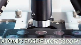
- 6. BASIC COMPONENTS • The basic components of an Atomic force microscope include : • Photo-detector and feedback control • Probe • Scanner • Cantilever and tip • Laser
- 7. PROBE
- 8. CANTILEVER
- 9. SCANNER
- 10. PHOTO DETECTOR AND FEEDBACK CONTROL
- 11. OVERVIEW OF COMPONENTS AND FUNCTIONS
- 12. PATHWAY
- 15. TAPPING MODE
- 16. NON CONTACT MODE
- 17. ADVANTAGES DISADVANTAGES ADVANTAGES AND DISADVANTAGES OF AFM ‣ Easy sample preparation. ‣ Non-destructive imaging. ‣ Accurate height information. ‣ Works in vacuum , air and liquids. ‣ Living systems can be studied. ‣ Sample not required to be conductive. ‣ Polymers , ceramics , glass , metals , ‣ Limited vertical range. ‣ Limited magnification range. ‣ Highly dependent on AFM probes. ‣ Tip or sample can be damaged.
- 18. APPLICATIONS A. Digitally images a topographical surface. B. Determines the roughness of a surface sample or to measure the thickness of a crystal growth layer. C. Any sample like ceramic material , human cells or individual molecules of DNA. D. In biological applications: 1.Study of unfolding particles 2.Imagining of biomolecules 3.Force measurements in real solvent environments 4.Antibody-Antigen Binding studies 5.Ligand-Receptor Binding studies 6.Binding Forces of complimentary DNA strands
- 20. SUMMARY • AFM stands for Atomic Force Microscopy. • It works by scanning a probe over the sample surface, building up a map of the height or topography of the surface as it goes along. • AFM microscopy is different from other microscopes as it physically feels the sample’s surface with a sharp probe , building up a map of the height of sample’s surface. • It provides single atomic level structure so provides high resolution. • It doesn’t need focusing , illumination , depth of field.
- 21. • Main components of the AFM instrument include: • Microscope stage : Moving AFM tip , Sample holder , Force sensor • Control electronics : Optical microscope , Vibration controller • Computer : The control electronics usually takes the form of a large box interfaced to both the microscope stage and the computer.
- 22. AFM has 3 basic modes of operation: 1. Contact mode : Strong , Repulsive • High Resolution Images • Fastest of all the topographic modes. • Sensitive to the nature of sample.
- 23. 2. Non-Contact Mode : Weak , Attractive • Oscillating modes can measure images with a small probe-sample force. 3. Tapping Mode : Strong , Repulsive • No Capillary effect. • Amplitude signals are used in feedback. • Used for imaging in air.