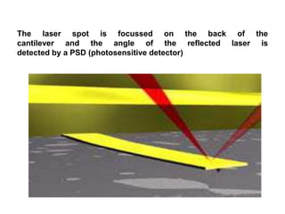
18PYB103J
SEMICONDUCTOR PHYSICS
MODULE 5
Atomic Force Microscopy
BY
Dr.T.BEENA
ASSISTANT PROFESSOR
DEPARTMENT OF PHYSICS
SRM IST, RAMAPURAM, CHENNAI – 600089
Scanning Probe Microscopes
(SPMs)
• Two types of microscopy
– Scanning Tunneling Microscope (STM)
– Atomic Force Microscope (AFM)
2
Atomic Force Microscopy
Definition of AFM
• The atomic force microscope (AFM) is a very high-
resolution type of scanning probe microscopy.
• Resolution is fractions of a nanometer.
• The AFM is one of the foremost tools for imaging,
measuring and manipulating matter at the nanoscale.
• The information is gathered by "feeling" the surface
with a mechanical probe.
Basic Arrangement & Alignment of AFM
The laser spot is focussed on the back of the
cantilever and the angle of the reflected laser is
detected by a PSD (photosensitive detector)
How It Works
http://www.molec.com/what_is_afm.html
• Invented in 1986
• Cantilever
• Tip
• Surface
• Laser
• Multi-segment photodetector
Figure 4. Three common types of AFM tip. (a) normal tip (3 µm tall); (b)
supertip; (c) Ultralever (also 3 µm tall). Electron micrographs by Jean-
Paul Revel, Caltech. Tips from Park Scientific Instruments; supertip
made by Jean-Paul Revel.
http://stm2.nrl.navy.mil/how-afm/how-afm.html#imaging%20modes
• AFM consist of micro scale cantilever with
a sharp tip and its end scan that is used to
scan the specimen surface .
• The cantilever is made up of silicon or
silicon nitride with a tip radius of curvature
on the order of nanometre.
Scanning Modes:
• 1.) Tapping/Contact Mode
• 2.) Non contact Mode
Non-Contact Mode
• Measures attractive forces between tip and
sample
• Tip doesn’t touch sample
• Van der Waals forces between tip and sample
detected
• Problems: Can’t use with samples in fluid
• Used to analyze semiconductors
• Doesn’t degrade or interfere with sample- better
for soft samples
Topography
• Contact Mode
– High resolution
– Damage to sample
– Can measure
frictional forces
• Non-Contact Mode
– Lower resolution
– No damage to
sample
• Tapping Mode
– Better resolution
– Minimal damage to
sample
13
Sources: http://www.almaden.ibm.com/vis/stm/blue.html
http://www.asylumresearch.com/ImageGallery/Mat/Mat.shtml#M7
Nickel from an STM ZnO from an AFM
Applications
• Study Unfolding Of Proteins
• Imagining Of Biomolecules
• Force Measurements In Real Solvent
Environments
• Antibody-Antigen Binding Studies
• Ligand-Receptor Binding Studies
• Binding Forces Of Complimentary DNA
Strands
• Study Surface Frictional Forces
• Ion Channel Localization
Various Application of AFM:
• 1.) Beam Deflection
• Detection
• 2.) Force Spectroscopy
• 3.) Nanolithography
• Using AFMs in Nanoscience
– Allows atom by atom (or clumps of atoms by
clumps of atoms) manipulation as shown by
the images below
16
Xenon atoms
Carbon monoxide molecules
Source: http://www.almaden.ibm.com/vis/stm/atomo.html
ADVANTAGES OF AFM
• The AFM has several advantages over the scanning
electron microscope (SEM). Unlike the electron
microscope which provides a two-dimensional
projection or a two-dimensional image of a sample, the
AFM provides a true three-dimensional surface profile.
• Additionally, samples viewed by AFM do not require
any special treatments (such as metal/carbon coatings)
that would irreversibly change or damage the sample.
While an electron microscope needs an expensive
vacuum environment for proper operation, most AFM
modes can work perfectly well in ambient air or even a
liquid environment.
• This makes it possible to study biological macromolecules and
even living organisms.
• In principle, AFM can provide higher resolution than SEM. It has
been shown to give true atomic resolution in ultra-high vacuum
(UHV) and, more recently, in liquid environments.
• High resolution AFM is comparable in resolution to Scanning
Tunneling Microscopy and Transmission Electron Microscopy.
DISADVANTAGES OF AFM
• A disadvantage of AFM compared with the scanning
electron microscope (SEM) is the image size. The SEM
can image an area on the order of millimetres by
millimetres with a depth of field on the order of
millimetres.
• The AFM can only image a maximum height on the
order of micrometres and a maximum scanning area of
around 150 by 150 micrometres.
DISADVANTAGES OF AFM
• Another inconvenience is that an incorrect choice of
tip for the required resolution can lead to image
artifacts.
• Traditionally the AFM could not scan images as fast
as an SEM, requiring several minutes for a typical
scan, while a SEM is capable of scanning at near
real-time (although at relatively low quality) after the
chamber is evacuated.
• The relatively slow rate of scanning during AFM
imaging often leads to thermal drift in the image

Atomic force microscopy

  • 1.
    18PYB103J SEMICONDUCTOR PHYSICS MODULE 5 AtomicForce Microscopy BY Dr.T.BEENA ASSISTANT PROFESSOR DEPARTMENT OF PHYSICS SRM IST, RAMAPURAM, CHENNAI – 600089
  • 2.
    Scanning Probe Microscopes (SPMs) •Two types of microscopy – Scanning Tunneling Microscope (STM) – Atomic Force Microscope (AFM) 2
  • 3.
  • 4.
    Definition of AFM •The atomic force microscope (AFM) is a very high- resolution type of scanning probe microscopy. • Resolution is fractions of a nanometer. • The AFM is one of the foremost tools for imaging, measuring and manipulating matter at the nanoscale. • The information is gathered by "feeling" the surface with a mechanical probe.
  • 6.
    Basic Arrangement &Alignment of AFM
  • 7.
    The laser spotis focussed on the back of the cantilever and the angle of the reflected laser is detected by a PSD (photosensitive detector)
  • 8.
    How It Works http://www.molec.com/what_is_afm.html •Invented in 1986 • Cantilever • Tip • Surface • Laser • Multi-segment photodetector Figure 4. Three common types of AFM tip. (a) normal tip (3 µm tall); (b) supertip; (c) Ultralever (also 3 µm tall). Electron micrographs by Jean- Paul Revel, Caltech. Tips from Park Scientific Instruments; supertip made by Jean-Paul Revel. http://stm2.nrl.navy.mil/how-afm/how-afm.html#imaging%20modes
  • 9.
    • AFM consistof micro scale cantilever with a sharp tip and its end scan that is used to scan the specimen surface . • The cantilever is made up of silicon or silicon nitride with a tip radius of curvature on the order of nanometre.
  • 10.
    Scanning Modes: • 1.)Tapping/Contact Mode • 2.) Non contact Mode
  • 11.
    Non-Contact Mode • Measuresattractive forces between tip and sample • Tip doesn’t touch sample • Van der Waals forces between tip and sample detected • Problems: Can’t use with samples in fluid • Used to analyze semiconductors • Doesn’t degrade or interfere with sample- better for soft samples
  • 12.
    Topography • Contact Mode –High resolution – Damage to sample – Can measure frictional forces • Non-Contact Mode – Lower resolution – No damage to sample • Tapping Mode – Better resolution – Minimal damage to sample
  • 13.
  • 14.
    Applications • Study UnfoldingOf Proteins • Imagining Of Biomolecules • Force Measurements In Real Solvent Environments • Antibody-Antigen Binding Studies • Ligand-Receptor Binding Studies • Binding Forces Of Complimentary DNA Strands • Study Surface Frictional Forces • Ion Channel Localization
  • 15.
    Various Application ofAFM: • 1.) Beam Deflection • Detection • 2.) Force Spectroscopy • 3.) Nanolithography
  • 16.
    • Using AFMsin Nanoscience – Allows atom by atom (or clumps of atoms by clumps of atoms) manipulation as shown by the images below 16 Xenon atoms Carbon monoxide molecules Source: http://www.almaden.ibm.com/vis/stm/atomo.html
  • 17.
    ADVANTAGES OF AFM •The AFM has several advantages over the scanning electron microscope (SEM). Unlike the electron microscope which provides a two-dimensional projection or a two-dimensional image of a sample, the AFM provides a true three-dimensional surface profile. • Additionally, samples viewed by AFM do not require any special treatments (such as metal/carbon coatings) that would irreversibly change or damage the sample. While an electron microscope needs an expensive vacuum environment for proper operation, most AFM modes can work perfectly well in ambient air or even a liquid environment.
  • 18.
    • This makesit possible to study biological macromolecules and even living organisms. • In principle, AFM can provide higher resolution than SEM. It has been shown to give true atomic resolution in ultra-high vacuum (UHV) and, more recently, in liquid environments. • High resolution AFM is comparable in resolution to Scanning Tunneling Microscopy and Transmission Electron Microscopy.
  • 19.
    DISADVANTAGES OF AFM •A disadvantage of AFM compared with the scanning electron microscope (SEM) is the image size. The SEM can image an area on the order of millimetres by millimetres with a depth of field on the order of millimetres. • The AFM can only image a maximum height on the order of micrometres and a maximum scanning area of around 150 by 150 micrometres.
  • 20.
    DISADVANTAGES OF AFM •Another inconvenience is that an incorrect choice of tip for the required resolution can lead to image artifacts. • Traditionally the AFM could not scan images as fast as an SEM, requiring several minutes for a typical scan, while a SEM is capable of scanning at near real-time (although at relatively low quality) after the chamber is evacuated. • The relatively slow rate of scanning during AFM imaging often leads to thermal drift in the image