This document is a tutorial on the 8051 microcontroller. It includes chapters that overview the 8051 architecture, provide a design example, and cover topics like interrupts, timers/counters, and the serial port. Reference materials are provided, such as books, websites, and a server location for additional information. A comparison is made between the low-power 8051 and more powerful Pentium processors. The 8051 chip features like two timers/counters and I/O ports are also detailed.


![ET4514 Digital Systems 2 Sample Questions 10/12/1999
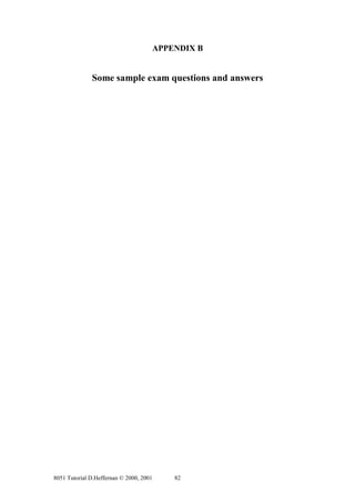
Q1 A simple 8-bit analog-to-digital converter device, as shown, is to be interfaced to an
8051 microcomputer. The READY line goes low when conversion data is available. The
READY line should be used to interrupt the 8051 microcontroller.
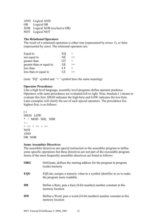
A/D
Vin Converter 8-bit
digital data
Ready
a) With the aid of a block diagram show how this device can be interfaced to the 8051. 10
b) Write an assembly language program which will capture 250 data samples from the 23
A/D converter and store this data in XDATA memory. The program is to be interrupt
driven.
Q2 [33 marks]
Write an 8051 assembly language program which will cause a timed program delay of n seconds,
where n can have a value between 1 and 255. The program design is to be based on the use of
nested subroutines which will include a one milli-second delay subroutine and a one second delay
subroutine. The program is to be based on software timing loops and it will not employ hardware
timers. Show all timing calculations and assumptions. Assume that the basic instruction cycle time
for the 8051 is 1 microsecond.
Q3 A simple burglar alarm system has 4 zone inputs connected to an 8051 I/O port. If any
one of these inputs is activated a bell will sound for 5 minutes and the corresponding zone
LED, or LEDS, will be activated.
a) With the aid of a diagram describe the hardware circuit for this alarm device. 10
b) Design an 8051 assembly language program to implement the required functionality 23
for this system.
8051 Tutorial D.Heffernan © 2000, 2001 83](https://image.slidesharecdn.com/8051tutorial-110522164309-phpapp01/85/8051-tutorial-83-320.jpg)


![Q2 [33 marks]
Write an 8051 assembly language program which will cause a timed program delay of n seconds,
where n can have a value between 1 and 255. The program design is to be based on the use of
nested subroutines which will include a one milli-second delay subroutine and a one second delay
subroutine. The program is to be based on software timing loops and it will not employ hardware
timers. Show all timing calculations and assumptions. Assume that the basic instruction cycle time
for the 8051 is 1 microsecond.
Q2 Sample Answer
Simple calculations for timing loops
No attempt is made to tune out minor inaccuracies due to code overhead
Inner loop
There is an inner loop in the ONE_MILLI_SUB subroutine which will cause a 4 microsecond
delay. Instruction execution times are taken from instruction set data which is given in the back of
the exam paper.
NOP 1
NOP 1
DJNZ R7, LOOP_1_MILLI 2
________________________________
4
ONE_MILLI_SUB
The ONE_MILLI_SUB subroutine simply executes the inner loop 250 times.
250 x 4 = 1000 microseconds = 1 milliseconds
ONE_SEC_SUB
The ONE_SEC_SUB subroutine has an inner loop which calls the ONE_MILLI_SUB
four times; giving an inner delay of 4 milliseconds. This 4 millisecond delay is called 250
times.
250 x 4 milliseconds = 1 second.
PROG_DELAY_SUB
The PROG_DELAY_SUB subroutine is called with a value 1..255 in the accumulator; to
cause the corresponding delay in seconds. If the accumulator has a value of zero the
subroutine immediately returns.
8051 Tutorial D.Heffernan © 2000, 2001 99](https://image.slidesharecdn.com/8051tutorial-110522164309-phpapp01/85/8051-tutorial-99-320.jpg)