SlideShare a Scribd company logo
Dr.Y.Narasimha MurthyPh.D
yayavaram@yahoo.com
1
UNIT-II ARM 7 Microcontroller
INTRODUCTION:
The ARM was originally developed at Acorn Computers Limited of Cambridge , England,
between 1983 and 1985. It was the first RISC microprocessor developed for commercial use and
has some significant differences from subsequent RISC architectures. In 1990 ARM Limited
was established as a separate company specifically to widen the exploitation of ARM technology
and it is established as a market-leader for low-power and cost-sensitive embedded
applications. The ARM is supported by a toolkit which includes an instruction set emulator for
hardware modelling and software testing and benchmarking, an assembler, C and C++
compilers, a linker and a symbolic debugger.
The 16-bit CISC microprocessors that were available in 1983 were slower than standard memory
parts. They also had instructions that took many clock cycles to complete (in some cases, many
hundreds of clock cycles), giving them very long interrupt latencies.As a result of these
frustrations with the commercial microprocessor offerings, the design of a proprietary
microprocessor was considered and ARM chip was designed.
ARM 7TDMI-S Processor : The ARM7TDMI-S processor is a member of the ARM family of
general-purpose 32-bit microprocessors. The ARM family offers high performance for very
low-power consumption and gate count. The ARM7TDMI-S processor has a Von Neumann
architecture, with a single 32-bit data bus carrying both instructions and data. Only load, store,
and swap instructions can access data from memory. The ARM7TDMI-S processor uses a three
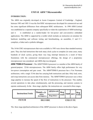
stage pipeline to increase the speed of the flow of instructions to the processor. This enables
several operations to take place simultaneously, and the processing, and memory systems to
operate continuously. In the three-stage pipeline the instructions are executed in three stages.
The three stage pipelined architecture of the ARM7 processor is shown in the above figure.
Dr.Y.Narasimha MurthyPh.D
yayavaram@yahoo.com
2
ARM7TDMIS stands for
T: THUMB ;
D for on-chip Debug support, enabling the processor to halt in response to a debug request,
M: enhanced Multiplier, yield a full 64-bit result, high performance
I: Embedded ICE hardware (In Circuit emulator)
S : Synthesizable
FEATURES OF ARM PROCESSORS
The ARM processors are based on RISC architectures and this architecture has provided small
implementations, and very low power consumption. Implementation size, performance, and very
low power consumption remain the key features in the development of the ARM devices.
The typical RISC architectural features of ARM are :
A large uniform register file
A load/store architecture, where data-processing operations only operate on register
contents, not directly on memory contents
Simple addressing modes, with all load/store addresses being determined from register
contents and instruction fields only uniform and fixed-length instruction fields, to
simplify instruction decode.
Control over both the Arithmetic Logic Unit (ALU) and shifter in most data-processing
instructions to maximize the use of an ALU and a shifter
Auto-increment and auto-decrement addressing modes to optimize program loops
Load and Store Multiple instructions to maximize data throughput
Conditional execution of almost all instructions to maximize execution throughput.
There are three basic instruction sets for ARM.
A 32- bit ARM instruction set
A 16 –bit Thumb instruction set and
The 8-bit Java Byte code used in Jazelle state
The Thumb instruction set is a subset of the most commonly used32-bit ARM
instructions.Thumb instructions operate with the standard ARM register configurations
,enabling excellent interoperability between ARM and Thumb states.This Thumb state is nearly
Dr.Y.Narasimha MurthyPh.D
yayavaram@yahoo.com
3
65% of the ARM code and can provide 160%of the performance of ARM code when working
ona 16-bit memory system. This Thumb mode is used in embedded systems where memory
resources are limited. The Jazelle mode is used in ARM9 processor to work with 8-bit Java
code.
ARCHITECTURE OF ARM PROCESSORS:
The ARM 7 processor is based on Von Neman model with a single bus for both data and
instructions..( The ARM9 uses Harvard model).Though this will decrease the performance of
ARM, it is overcome by the pipe line concept. ARM uses the Advanced Microcontroller Bus
Architecture (AMBA) bus architecture. This AMBA include two system buses: the AMBA
High-Speed Bus (AHB) or the Advanced System Bus (ASB), and the Advanced Peripheral Bus
(APB).
The ARM processor consists of
Arithmetic Logic Unit (32-bit)
One Booth multiplier(32-bit)
One Barrel shifter
One Control unit
Register file of 37 registers each of 32 bits.
In addition to this the ARM also consists of a Program status register of 32 bits, Some
special registers like the instruction register, memory data read and write register and
memory address register ,one Priority encoder which is used in the multiple load and
store instruction to indicate which register in the register file to be loaded or stored and
Multiplexers etc.
Dr.Y.Narasimha MurthyPh.D
yayavaram@yahoo.com
4
ARM Registers : ARM has a total of 37 registers .In which - 31 are general-purpose registers
of 32-bits, and six status registers .But all these registers are not seen at once. The processor
state and operating mode decide which registers are available to the programmer. At any time,
among the 31 general purpose registers only 16 registers are available to the user. The remaining
15 registers are used to speed up exception processing. there are two program status registers:
CPSR and SPSR (the current and saved program status registers, respectively
In ARM state the registers r0 to r13 are orthogonal—any instruction that you can apply to r0 you
can equally well apply to any of the other registers.
The main bank of 16 registers is used by all unprivileged code. These are the User mode
registers. User mode is different from all other modes as it is unprivileged. In addition to this
register bank ,there is also one 32-bit Current Program status Register(CPSR)
Dr.Y.Narasimha MurthyPh.D
yayavaram@yahoo.com
5
In the 15 registers ,the r13 acts as a stack pointer register and r14 acts as a link register and r15
acts as a program counter register.
Register r13 is the sp register ,and it is used to store the address of the stack top. R13 is used by
the PUSH and POP instructions in T variants, and by the SRS and RFE instructions from
ARMv6.
Register 14 is the Link Register (LR). This register holds the address of the next instruction after
a Branch and Link (BL or BLX) instruction, which is the instruction used to make a subroutine
call. It is also used for return address information on entry to exception modes. At all other times,
R14 can be used as a general-purpose register.
Register 15 is the Program Counter (PC). It can be used in most instructions as a pointer to the
instruction which is two instructions after the instruction being executed.
The remaining 13 registers have no special hardware purpose.
CPSR : The ARM core uses the CPSR register to monitor and control internal operations. The
CPSR is a dedicated 32-bit register and resides in the register file. The CPSR is divided into
four fields, each of 8 bits wide : flags, status, extension, and control. The extension and status
fields are reserved for future use. The control field contains the processor mode, state, and
interrupt mask bits. The flags field contains the condition flags. The 32-bit CPSR register is
shown below.
Dr.Y.Narasimha MurthyPh.D
yayavaram@yahoo.com
6
Processor Modes: There are seven processor modes .Six privileged modes abort, fast interrupt
request, interrupt request, supervisor, system, and undefined and one non-privileged mode
called user mode.
The processor enters abort mode when there is a failed attempt to access memory. Fast interrupt
request and interrupt request modes correspond to the two interrupt levels available on the ARM
processor. Supervisor mode is the mode that the processor is in after reset and is generally the
mode that an operating system kernel operates in. System mode is a special version of user mode
that allows full read-write access to the CPSR. Undefined mode is used when the processor
encounters an instruction that is undefined or not supported by the implementation. User mode is
used for programs and applications.
Banked Registers : Out of the 32 registers , 20 registers are hidden from a program at different
times. These registers are called banked registers and are identified by the shading in the
diagram. They are available only when the processor is in a particular mode; for example, abort
mode has banked registers r13_abt , r14_abt and spsr _abt. Banked registers of a particular
mode are denoted by an underline character post-fixed to the mode mnemonic or _mode.
When the T bit is 1, then the processor is in Thumb state. To change states the core executes a
specialized branch instruction and when T= 0 the processor is in ARM state and executes ARM
instructions. There are two interrupt request levels available on the ARM processor core—
interrupt request (IRQ) and fast interrupt request (FIQ).
V, C , Z , N are the Condition flags .
V (oVerflow) : Set if the result causes a signed overflow
C (Carry) : Is set when the result causes an unsigned carry
Z (Zero) : This bit is set when the result after an arithmetic operation is zero, frequently
used to indicate equality
N (Negative) : This bit is set when the bit 31 of the result is a binary 1.
PIPE LINE : Pipeline is the mechanism used by the RISC processor to execute instructions at
an increased speed. This pipeline speeds up execution by fetching the next instruction while
other instructions are being decoded and executed. During the execution of an instruction ,the
processor Fetches the instruction .It means loads an instruction from memory.And decodes the
Dr.Y.Narasimha MurthyPh.D
yayavaram@yahoo.com
7
instruction i.e identifies the instruction to be executed and finally Executes the instruction and
writes the result back to a register.
The ARM7 processor has a three stage pipelining architecture namely Fetch , Decode and
Execute.And the ARM 9 has five stage Pipe line architecture.The three stage pipelining is
explained as below.
To explain the pipelining ,let us consider that there are three instructions Compare, Subtract and
Add.The ARM7 processor fetches the first instruction CMP in the first cycle and during the
second cycle it decodes the CMP instruction and at the same time it will fetch the SUB
instruction. During the third cycle it executes the CMP instruction , while decoding the SUB
instruction and also at the same time will fetch the third instruction ADD. This will improve the
speed of operation. This leads to the concept of parallel processing .This pipeline example is
shown in the following diagram.
Dr.Y.Narasimha MurthyPh.D
yayavaram@yahoo.com
8
As the pipeline length increases, the amount of work done at each stage is reduced, which allows
the processor to attain a higher operating frequency. This in turn increases the performance. One
important feature of this pipeline is the execution of a branch instruction or branching by the
direct modification of the PC causes the ARM core to flush its pipeline.
Exceptions, Interrupts, and the Vector Table :
Exceptions are generated by internal and external sources to cause the ARM processor to handle
an event, such as an externally generated interrupt or an attempt to execute an Undefined
instruction. The processor state just before handling the exception is normally preserved so that
the original program can be resumed after the completion of the exception routine. More than
one exception can arise at the same time.ARM exceptions may be considered in three groups
1. Exceptions generated as the direct effect of executing an instruction.Software interrupts,
undefined instructions (including coprocessor instructions where the requested coprocessor is
absent) and prefetch aborts (instructions that are invalid due to a memory fault occurring during
fetch) come under this group.
2. Exceptions generated as a side-effect of an instruction.Data aborts (a memory fault during a
load or store data access) are in this group.
3. Exceptions generated externally, unrelated to the instruction flow.Reset, IRQ and FIQ are in
this group.
The ARM architecture supports seven types of exceptions.
i.Reset
ii.Undefined Instruction
iii.Software Interrupt(SWI)
iv. Pre-fetch abort(Instruction Fetch memory fault)
v.Data abort (Data access memory fault)
vi. IRQ(normal Interrupt)
vii. FIQ (Fast Interrupt request).
When an Exception occurs , the processor performs the following sequence of actions:
• It changes to the operating mode corresponding to the particular exception.
• It saves the address of the instruction following the exception entry instruction in r14 of the
new mode.
Dr.Y.Narasimha MurthyPh.D
yayavaram@yahoo.com
9
• It saves the old value of the CPSR in the SPSR of the new mode.
• It disables IRQs by setting bit 7 of the CPSR and, if the exception is a fast interrupt, disables
further fast interrupts by setting bit 6 of the CPSR.
• It forces the PC to begin executing at the relevant vector address
Excdption / Interrupt Name Address High Address
Reset RESET 0X00000000 0Xffff0000
Undefined Instruction UNDEF 0X00000004 0Xffff0004
Software Interrupt SWI 0X00000008 0Xffff0008
Pre-fetch Abort PABT 0X0000000C 0Xffff000c
Data Abort DABT 0X00000010 0Xffff0010
Reserved --- 0X00000014 0Xffff0014
Interrupt Request IRQ 0X00000018 0Xffff0018
Fast Interrupt Request FIQ 0X0000001C 0Xffff001c
The exception Vector table shown above gives the address of the subroutine program to be
executed when the exception or interrupt occurs. Each vector table entry contains a form of
branch instruction pointing to the start of a specific routine.
Reset vector is the location of the first instruction executed by the processor when power is
applied. This instruction branches to the initialization code.
Undefined instruction vector is used when the processor cannot decode an instruction.
Software interrupt vector is called when you execute a SWI instruction. The SWI instruction is
frequently used as the mechanism to invoke an operating system routine.
Pre-fetch abort vector occurs when the processor attempts to fetch an instruction from an address
without the correct access permissions. The actual abort occurs in the decode stage.
Data abort vector is similar to a prefetch abort but is raised when an instruction attempts to
access data memory without the correct access permissions.
Interrupt request vector is used by external hardware to interrupt the normal execution flow of
the processor. It can only be raised if IRQs are not masked in the CPSR.
ARM Processor Families
There are various ARM processors available in the market for different application .These are
grouped into different families based on the core .These families are based on the ARM7,
Dr.Y.Narasimha MurthyPh.D
yayavaram@yahoo.com
10
ARM9, ARM10, and ARM11 cores. The numbers 7, 9, 10, and 11 indicate different core
designs. The ascending number indicates an increase in performance and sophistication.
Though ARM 8 was introduced during 1996, it is no more available in the market. The
following table gives a brief comparison of their performance and available resources.
The ARM7 core has a Von Neumann–style architecture, where both data and instructions use the
same bus. The core has a three-stage pipeline and executes the architecture ARMv4T instruction
set. The ARM7TDMI was introduced in 1995 by ARM. It is currently a very popular core and is
used in many 32-bit embedded processors.
The ARM9 family was released in 1997. It has five stage pipeline architecture .Hence , the
ARM9 processor can run at higher clock frequencies than the ARM7 family. The extra stages
improve the overall performance of the processor. The memory system has been redesigned to
follow the Harvard architecture, with separate data and instruction .buses. The first processor in
the ARM9 family was the ARM920T, which includes a separate D + I cache and an MMU. This
processor can be used by operating systems requiring virtual memory support. ARM922T is a
variation on the ARM920T but with half the D +I cache size.
The latest core in the ARM9 product line is the ARM926EJ-S synthesizable processor core,
announced in 2000. It is designed for use in small portable Java-enabled devices such as 3G
phones and personal digital assistants (PDAs).
The ARM10 was released in 1999 . It extends the ARM9 pipeline to six stages. It also supports
an optional vector floating-point (VFP) unit, which adds a seventh stage to the ARM10 pipeline.
The VFP significantly increases floating-point performance and is compliant with the IEEE
754.1985 floating-point standard.
The ARM1136J-S is the ARM11 processor released in the year 2003 and it is designed for high
performance and power efficient applications. ARM1136J-S was the first processor
implementation to execute architecture ARMv6 instructions. It incorporates an eight-stage
pipeline with separate load store and arithmetic pipelines.
A brief comparison of different ARM families is presented below.
Dr.Y.Narasimha MurthyPh.D
yayavaram@yahoo.com
11
ARM
Family
Year of
Release
Architecture Pipeline Operational
Frequency
Multiplier MIPS
ARM7 1995 Von Neumann 3 stage 80 M.Hz 8x32 0.97
ARM9 1997 Harvard 5 stage 150M.Hz 8x32 1.1
ARM10 1999 Harvard 6 stage 260M.Hz 16x32 1.3
ARM11 2003 Harvard 8 stage 335M.Hz 16x32 1.2
ARM INSTRUCTION SET
ARM instructions process data held in registers and only access memory with load and store
instructions. ARM instructions commonly take two or three operands.
For example ,the ADD instruction adds the two values stored in registers r1 and r2 (the source
registers). It stores the result to register r3 (the destination register). ADD r3, r1, r2
ARM instructions are classified into data processing instructions, branch instructions, load-store
instructions, software interrupt instruction, and program status register instructions.
Data Processing Instructions :
The data processing instructions manipulate data within registers. They are move instructions,
Arithmetic instructions, logical instructions, comparison instructions, and multiply instructions.
Most data processing instructions can process one of their operands using the barrel shifter.
Data processing instructions are processed within the arithmetic logic unit (ALU). A unique and
powerful feature of the ARM processor is the ability to shift the 32-bit binary pattern in one of
the source registers left or right by a specific number of positions before it enters the ALU. This
shift increases the power and flexibility of many data processing operations.
There are data processing instructions that do not use the barrel shift, for example, the MUL
(multiply), CLZ (count leading zeros), and QADD (signed saturated 32-bit add) instructions.
i.Move Instructions : Move instruction copies R into a destination register Rd, where R is a
register or immediate value. This instruction is useful for setting initial values and transferring
data between registers.
Dr.Y.Narasimha MurthyPh.D
yayavaram@yahoo.com
12
Example1 : PRE r5 = 5
r7 = 8
MOV r7, r5 ;
POST r5 = 5
r7 = 5
The MOV instruction takes the contents of register r5 and copies them into register r7.
Example 2: MOVS r0, r1, LSL #1
MOVS instruction shifts register r1 left by one bit
Arithmetic Instructions : The arithmetic instructions implement addition and subtraction of
32-bit signed and unsigned values. the various addition and subtraction instructions are given in
table below.
SUB r0, r1, r2 ; This subtract instruction subtracts a value stored in register r2 from a value
stored in register r1. The result is stored in register r0.
RSB r0, r1, #0 ; This reverse subtract instruction (RSB) subtracts r1 from the constant value #0,
writing. the result to r0. You can use this instruction to negate numbers.
SUBS r1, r1, #1 ; The SUBS instruction is useful for decrementing loop counters. In this
example we subtract the immediate value one from the value one stored in
register r1. The result value zero is written to register r1.
Logical Instructions : These Logical instructions perform bitwise logical operations on the two
source registers.
Dr.Y.Narasimha MurthyPh.D
yayavaram@yahoo.com
13
BIC r0, r1, r2 ; BIC, carries out a logical bit clear. register r2 contains a binary pattern where
every binary 1 in r2 clears a corresponding bit location in register r1. This instruction is
particularly useful when clearing status bits and is frequently used to change interrupt masks in
the cpsr.
Comparison Instructions : The comparison instructions are used to compare or test a
register with a 32-bit value. This instruction affects only CPSR register flags.
Branch Instructions: A branch instruction changes the normal flow of execution of a main
program or is used to call a subroutine routine. This type of instruction allows programs to have
subroutines, if-then-else structures, and loops. The change of execution flow forces the program
counter pc to point to a new address.
Example 1: B forward ; (unconditional branch to forward)
ADD r1, r2, #4 ;
ADD r0, r6, #2 ;
ADD r3, r7, #4 ;
forward SUB r1, r2, #4 ;
Similarly Backward branch :
Dr.Y.Narasimha MurthyPh.D
yayavaram@yahoo.com
14
backward : ADD r1, r2, #4 ;
SUB r1, r2, #4 ;
ADD r4, r6, r7 ;
B backward ; branch to the target backward.
The branch with link, or BL, instruction is similar to the B instruction but overwrites the
link register lr with a return address. It performs a subroutine call.
BL subroutine ; branch to subroutine
CMP r1, #5 ; compare r1 with 5
MOVEQ r1, #0 ; if (r1==5) then r1 = 0 :
Subroutine
MOV pc, lr ; return by moving pc = lr
The Branch Exchange (BX) and Branch Exchange with Link (BLX) are the third type of branch instruction.
The BX instruction uses an absolute address stored in register Rm. It is primarily used to branch to and
from Thumb code. The T bit in the cpsr is updated by the least significant bit of the branch register.
Similarly the BLX instruction updates the T bit of the cpsr with the least significant bit and additionally
sets the link register with the return address.
The details of the branch instructions are given in the table above.
Load-Store Instructions : Load-store instructions transfer data between memory and processor
registers. There are three types of load-store instructions:
Single-register transfer
Multiple-register transfer, and
Dr.Y.Narasimha MurthyPh.D
yayavaram@yahoo.com
15
Swap.
Single-Register Transfer : These instructions are used for moving a single data item in and out of a
register. The data types supported are signed and unsigned words (32-bit), half-words (16-bit), and
bytes. Ex1: STR r0, [r1] ; = STR r0, [r1, #0] ; store the contents of register r0 to the
memory address pointed to by register r1.
Ex2 : LDR r0, [r1] ; = LDR r0, [r1, #0] ; load register r0 with the contents of the
memory address pointed to by register r1.
Multiple-Register Transfer : Load-store multiple instructions can transfer multiple registers
between memory and the processor in a single instruction. The transfer occurs from a base
address register Rn pointing into memory. Multiple-register transfer instructions are more
efficient than single-register transfers for moving blocks of data around memory and saving and
restoring context and stacks.
Load-store multiple instructions can increase interrupt latency. ARM implementations do not
usually interrupt instructions while they are executing. For example, on an ARM7 a load
multiple instruction takes 2 + N.t cycles, where N is the number of registers to load and t is the
number of cycles required for each sequential access to memory. If an interrupt has been raised,
then it has no effect until the load-store multiple instruction is complete.
Example 1: LDMIA r0!, {r1-r3} ; In this example, register r0 is the base register Rn and is
followed by !, indicating that the register is updated after the instruction is executed. In this case
the range is from register r1 to r3.
Example 2 : LDMIB : load multiple and increment before
Ex 3: LDMIB r0!, {r1-r3} ;
Ex 4 : LDMDA r0!, {r1-r3}
Dr.Y.Narasimha MurthyPh.D
yayavaram@yahoo.com
16
Stack Operations : The ARM architecture uses the load-store multiple instructions to carry out
stack operations. The pop operation (removing data from a stack) uses a load multiple
instruction; similarly, the push operation (placing data onto the stack) uses a store multiple
instruction.
A stack is either ascending (A) or descending (D). Ascending stacks grow towards higher
memory addresses; in contrast, descending stacks which grow towards lower memory addresses.
When a full stack (F)is used , the stack pointer sp points to an address that is the last used or full
location (i.e., sp points to the last item on the stack). In contrast, if an empty stack (E) is used ,
the sp points to an address that is the first unused or empty location (i.e., it points after the last
item on the stack).
Example1 : The STMFD instruction pushes registers onto the stack, updating the sp.
STMFD sp! , {r1,r4}; Store Multiple Full Descending Stack
PRE r1 = 0x00000002
r4 = 0x00000003
sp = 0x00080014
POST r1 = 0x00000002
r4 = 0x00000003
sp = 0x0008000c.
The stack operation is shown by the following diagram.
Example2: The STMED instruction pushes the registers onto the stack but updates register sp to
point to the next empty location as shown in the below diagram..
Dr.Y.Narasimha MurthyPh.D
yayavaram@yahoo.com
17
PRE r1 = 0x00000002
r4 = 0x00000003
sp = 0x00080010
STMED sp! , {r1,r4} ; Store Multiple Empty Descending Stack
POST r1 = 0x00000002
r4 = 0x00000003
sp = 0x00080008
This operation is explained in the following figure.
Swap Instruction :
The Swap instruction is a special case of a load-store instruction. It swaps (Similar to exchange)
the contents of memory with the contents of a register. This instruction is an atomic operation—
it reads and writes a location in the same bus operation, preventing any other instruction from
reading or writing to that location until it completes.Swap cannot be interrupted by any other
instruction or any other bus access. So, the system ―holds the bus‖ until the transaction is
complete.
Ex 1: SWP : Swap a word between memory and a register tmp = mem32[Rn]
mem32[Rn] =Rm
Rd = tmp
Ex2 : SWPB Swap a byte between memory and a register tmp = mem8[Rn]
mem8[Rn] =Rm
Dr.Y.Narasimha MurthyPh.D
yayavaram@yahoo.com
18
Rd = tmp.
Ex 3: SWP r0, r1, [r2] ; The swap instruction loads a word from memory into register
r0 and overwrites the memory with register r1.
Software Interrupt Instruction : A software interrupt instruction (SWI) is used to generate a
software interrupt exception, which can be used to call operating system routines.When the
processor executes an SWI instruction, it sets the program counter pc to the offset 0x8 in the
vector table. The instruction also forces the processor mode to SVC, which allows an operating
system routine to be called in a privileged mode. Each SWI instruction has an associated SWI
number, which is used to represent a particular function call or feature.
Ex: 0x00008000 SWI 0x123456
Here 0x123456, is the SWI number used by ARM toolkits as a debugging SWI. Typically
the SWI instruction is executed in user mode.
Program Status Register Instructions : There are two instructions available to directly control
a program status register (PSR). The MRS instruction transfers the contents of either the CPSR
or SPSR into a register.Similarly the MSR instruction transfers the contents of a register into
the CPSR or SPSR .These instructions together are used to read and write the CPSR and
SPSR.
MRS : copy program status register to a general-purpose register , Rd= PSR
MSR : move a general-purpose register to a program status register, PSR[field]=Rm
MSR : move an immediate value to a program status register, PSR[field]=immediate
Ex : MRS r1, CPSR
BIC r1, r1, #0x80 ; 0b01000000
MSR CPSR_C, r1.
The MSR first copies the CPSR into register r1. The BIC instruction clears bit 7 of r1. Register
r1 is then copied back into the CPSR, which enables IRQ interrupts. Here the code preserves all
the other settings in the CPSR intact and only modifies the I bit in the control field.
Dr.Y.Narasimha MurthyPh.D
yayavaram@yahoo.com
19
Loading Constants : In ARM instruction set there are no instructions to move the 32-bit
constant into a register. Since ARM instructions are 32 bits in size, they obviously cannot
specify a general 32-bit constant. To overcome this problem .two pseudo instructions are
provided to move a 32-bit value into a register.
LDR : load constant pseudo instruction Rd= 32-bit constant.
ADR : load address pseudo instruction Rd=32-bit relative address.
The first pseudo instruction writes a 32-bit constant to a register using whatever instructions are
available.
The second pseudo instruction writes a relative address into a register, which will be encoded
using a PC -relative expression.
Example 2: LDR r0, [pc, #constant_number-8-{PC}]
constant _number DCD 0xff00ffff.
Here the LDR instruction loads a 32-bit constant 0xff00ffff into register r0.
Example 3: The same constant can be loaded into the register r0 using the MVN instruction also.
MVN r0, #0x00ff0000
After execution r0 = 0xff00ffff.
Introduction to Thumb instruction set : Thumb encodes a subset of the 32-bit ARM
instructions into a 16-bit instruction set space. Since Thumb has higher performance than ARM
on a processor with a 16-bit data bus, but lower performance than ARM on a 32-bit data bus, use
Thumb for memory-constrained systems. Thumb has higher code density—the space taken up in
memory by an executable program—than ARM. For memory-constrained embedded systems,
for example, mobile phones and PDAs, code density is very important. Cost pressures also limit
memory size, width, and speed.
Thumb execution is flagged by the T bit (bit [5] ) in the CPSR. A Thumb implementation of the
same code takes up around 30% less memory than the equivalent ARM implementation. Even
though the Thumb implementation uses more instructions ; the overall memory footprint is
reduced. Code density was the main driving force for the Thumb instruction set. Because it was
also designed as a compiler target, rather than for hand-written assembly code. Below example
explains the difference between ARM and Thumb code
Dr.Y.Narasimha MurthyPh.D
yayavaram@yahoo.com
20
From the above example it is clear that the Thumb code is more denser than the ARM code.
Exceptions generated during Thumb execution switch to ARM execution before executing the
exception handler . The state of the T bit is preserved in the SPSR, and the LR of the exception
mode is set so that the normal return instruction performs correctly, regardless of whether the
exception occurred during ARM or Thumb execution.
In Thumb state, all the registers can not be accessed . Only the low registers r0 to r7 can be
accessed. The higher registers r8 to r12 are only accessible with MOV, ADD, or CMP
instructions. CMP and all the data processing instructions that operate on low registers update
the condition flags in the CPSR
The list of registers and their accessibility in Thumb mode are shown in the following table..
S.No Registers Access
1 r0 – r7 Fully accessible
2 r8 – r12 Only accessible by MOV ,ADD &CMP
3 r13SP Limited accessibility
4 r14 lr Limited accessibility
5 r15 PC Limited accessibility
6 CPSR Only indirect access
7 SPSR No access
Dr.Y.Narasimha MurthyPh.D
yayavaram@yahoo.com
21
Form the above discussion, it is clear that there are no MSR and MRS equivalent Thumb
instructions. To alter the CPSR or SPSR , one must switch into ARM state to use MSR and
MRS. Similarly, there are no coprocessor instructions in Thumb state. You need to be in ARM
state to access the coprocessor for configuring cache and memory management.
ARM-Thumb interworking is the method of linking ARM and Thumb code together for both
assembly and C/C++. It handles the transition between the two states. To call a Thumb routine
from an ARM routine, the core has to change state. This is done with the T bit of CPSR . The
BX and BLX branch instructions cause a switch between ARM and Thumb state while branching
to a routine. The BX lr instruction returns from a routine, also with a state switch if necessary.
The data processing instructions manipulate data within registers. They include move
instructions, arithmetic instructions, shifts, logical instructions, comparison instructions, and
multiply instructions. The Thumb data processing instructions are a subset of the ARM data
processing instructions.
Exs : ADC : add two 32-bit values and carry Rd = Rd + Rm + C flag
ADD : add two 32-bit values Rd = Rn + immediate
Rd = Rd + immediate
Rd = Rd + Rm
AND : logical bitwise AND of two 32-bit values Rd = Rd & Rm
ASR : arithmetic shift right Rd = Rm_immediate,
C flag= Rm[immediate − 1]
Rd = Rd_Rs, C flag = Rd[Rs - 1]
BIC : logical bit clear (AND NOT) of two 32-bit Rd = Rd AND
NOT(Rm)values
CMN : compare negative two 32-bit values Rn + Rm sets flags
CMP : compare two 32-bit integers Rn−immediate sets flags Rn−Rm sets flags
EOR : logical exclusive OR of two 32-bit values Rd = Rd EOR Rm
LSL : logical shift left Rd = Rm_ immediate,
C flag= Rm[32 − immediate]
Rd = Rd_Rs, C flag = Rd[32 − Rs]
LSR : logical shift right Rd = Rm_ immediate,
C flag = Rd [immediate − 1]
Rd = Rd_ Rs, C flag = Rd[Rs − 1]
MOV : move a 32-bit value into a register Rd = immediate
Dr.Y.Narasimha MurthyPh.D
yayavaram@yahoo.com
22
Rd = Rn
Rd = Rm
MUL : multiply two 32-bit values Rd = (Rm * Rd)[31:0]
MVN : move the logical NOT of a 32-bit value into a register Rd = NOT(Rm)
NEG : negate a 32-bit value Rd = 0 − Rm
ORR : logical bitwise OR of two 32-bit values Rd = Rd OR Rm
ROR : rotate right a 32-bit value Rd = Rd RIGHT_ROTATE Rs,
C flag= Rd[Rs−1]
SBC : subtract with carry a 32-bit value Rd = Rd − Rm − NOT(C flag)
SUB : subtract two 32-bit values Rd = Rn − immediate
Rd = Rd − immediate
Rd = Rn − Rm
sp = sp − (immediate_2)
TST : test bits of a 32-bit value Rn AND Rm sets flags
Note : Thumb deviates from the ARM style in that the barrel shift operations (ASR, LSL, LSR,
and ROR) are separate instructions.
Thankful to the following people for their invaluable information .
References : 1. ARM System Developer’s Guide Designing and Optimizing System Software –
Andrew N. Sloss , Dominic Symes and Chris Wright.
2. ARM-System on-Chip Architecture – Steve Furber.
3. ARM Architecture Reference Manual Copyright © 1996-1998, 2000, 2004, 2005
ARM Limited.

More Related Content

What's hot

ARM Architecture
ARM ArchitectureARM Architecture
ARM Architecture
Kshitij Gorde
 
ARM Processors
ARM ProcessorsARM Processors
ARM Processors
Mathivanan Natarajan
 
Arm
ArmArm
Lect 4 ARM PROCESSOR ARCHITECTURE
Lect 4 ARM PROCESSOR ARCHITECTURELect 4 ARM PROCESSOR ARCHITECTURE
Lect 4 ARM PROCESSOR ARCHITECTURE
Dr.YNM
 
Arm processor
Arm processorArm processor
Arm processor
PrashantSingh056
 
Arm modes
Arm modesArm modes
Arm modes
abhi165
 
EMBEDDED SYSTEM DESIGN ARM architecture support for operating system by sanj...
 EMBEDDED SYSTEM DESIGN ARM architecture support for operating system by sanj... EMBEDDED SYSTEM DESIGN ARM architecture support for operating system by sanj...
EMBEDDED SYSTEM DESIGN ARM architecture support for operating system by sanj...
D Y PATIL COLLEGE OF ENGINEERING PUNE
 
Arm architecture overview
Arm architecture overviewArm architecture overview
Arm architecture overview
Sunil Thorat
 
Arm arc-2016
Arm arc-2016Arm arc-2016
Arm arc-2016
Mohammed Gomaa
 
ARM7TDM
ARM7TDMARM7TDM
ARM7TDM
Ramasubbu .P
 
Arm architecture
Arm architectureArm architecture
Arm architecture
MinYeop Na
 
Lect 3 ARM PROCESSOR ARCHITECTURE
Lect 3  ARM PROCESSOR ARCHITECTURE Lect 3  ARM PROCESSOR ARCHITECTURE
Lect 3 ARM PROCESSOR ARCHITECTURE
Dr.YNM
 
Arm cortex-m3 by-joe_bungo_arm
Arm cortex-m3 by-joe_bungo_armArm cortex-m3 by-joe_bungo_arm
Arm cortex-m3 by-joe_bungo_arm
Prashant Ahire
 
Unit II Arm7 Thumb Instruction
Unit II Arm7 Thumb InstructionUnit II Arm7 Thumb Instruction
Unit II Arm7 Thumb Instruction
Dr. Pankaj Zope
 
Arm Lecture
Arm LectureArm Lecture
Arm Lecture
anishgoel
 
ARM- Programmer's Model
ARM- Programmer's ModelARM- Programmer's Model
ARM- Programmer's Model
Ravikumar Tiwari
 
LECT 1: ARM PROCESSORS
LECT 1: ARM PROCESSORSLECT 1: ARM PROCESSORS
LECT 1: ARM PROCESSORS
Dr.YNM
 
Arm corrected ppt
Arm corrected pptArm corrected ppt
Arm corrected ppt
anish jagan
 
ARM Processor
ARM ProcessorARM Processor
ARM Processor
Aniket Thakur
 
Arm architecture chapter2_steve_furber
Arm architecture chapter2_steve_furberArm architecture chapter2_steve_furber
Arm architecture chapter2_steve_furber
asodariyabhavesh
 

What's hot (20)

ARM Architecture
ARM ArchitectureARM Architecture
ARM Architecture
 
ARM Processors
ARM ProcessorsARM Processors
ARM Processors
 
Arm
ArmArm
Arm
 
Lect 4 ARM PROCESSOR ARCHITECTURE
Lect 4 ARM PROCESSOR ARCHITECTURELect 4 ARM PROCESSOR ARCHITECTURE
Lect 4 ARM PROCESSOR ARCHITECTURE
 
Arm processor
Arm processorArm processor
Arm processor
 
Arm modes
Arm modesArm modes
Arm modes
 
EMBEDDED SYSTEM DESIGN ARM architecture support for operating system by sanj...
 EMBEDDED SYSTEM DESIGN ARM architecture support for operating system by sanj... EMBEDDED SYSTEM DESIGN ARM architecture support for operating system by sanj...
EMBEDDED SYSTEM DESIGN ARM architecture support for operating system by sanj...
 
Arm architecture overview
Arm architecture overviewArm architecture overview
Arm architecture overview
 
Arm arc-2016
Arm arc-2016Arm arc-2016
Arm arc-2016
 
ARM7TDM
ARM7TDMARM7TDM
ARM7TDM
 
Arm architecture
Arm architectureArm architecture
Arm architecture
 
Lect 3 ARM PROCESSOR ARCHITECTURE
Lect 3  ARM PROCESSOR ARCHITECTURE Lect 3  ARM PROCESSOR ARCHITECTURE
Lect 3 ARM PROCESSOR ARCHITECTURE
 
Arm cortex-m3 by-joe_bungo_arm
Arm cortex-m3 by-joe_bungo_armArm cortex-m3 by-joe_bungo_arm
Arm cortex-m3 by-joe_bungo_arm
 
Unit II Arm7 Thumb Instruction
Unit II Arm7 Thumb InstructionUnit II Arm7 Thumb Instruction
Unit II Arm7 Thumb Instruction
 
Arm Lecture
Arm LectureArm Lecture
Arm Lecture
 
ARM- Programmer's Model
ARM- Programmer's ModelARM- Programmer's Model
ARM- Programmer's Model
 
LECT 1: ARM PROCESSORS
LECT 1: ARM PROCESSORSLECT 1: ARM PROCESSORS
LECT 1: ARM PROCESSORS
 
Arm corrected ppt
Arm corrected pptArm corrected ppt
Arm corrected ppt
 
ARM Processor
ARM ProcessorARM Processor
ARM Processor
 
Arm architecture chapter2_steve_furber
Arm architecture chapter2_steve_furberArm architecture chapter2_steve_furber
Arm architecture chapter2_steve_furber
 

Similar to Unitii armarchitecture-130305014346-phpapp01

ARM 7 and 9 Core Architecture Illustration
ARM 7 and 9 Core Architecture IllustrationARM 7 and 9 Core Architecture Illustration
ARM 7 and 9 Core Architecture Illustration
Jason J Pulikkottil
 
Unit 4 _ ARM Processors .pptx
Unit 4 _ ARM Processors .pptxUnit 4 _ ARM Processors .pptx
Unit 4 _ ARM Processors .pptx
VijayKumar201823
 
ARM
ARM ARM
Comparison between RISC architectures: MIPS, ARM and SPARC
Comparison between RISC architectures: MIPS, ARM and SPARCComparison between RISC architectures: MIPS, ARM and SPARC
Comparison between RISC architectures: MIPS, ARM and SPARC
Apurv Nerlekar
 
Introduction to arm architecture
Introduction to arm architectureIntroduction to arm architecture
Introduction to arm architecture
Zakaria Gomaa
 
arm
 arm arm
Unit ii arm7 thumb
Unit ii arm7 thumbUnit ii arm7 thumb
Unit ii arm7 thumb
Dr. Pankaj Zope
 
Arm architechture
Arm architechtureArm architechture
Arm architechture
Tanmay Gadani
 
Introduction to arm processor
Introduction to arm processorIntroduction to arm processor
Introduction to arm processor
RAMPRAKASHT1
 
arm_3.ppt
arm_3.pptarm_3.ppt
arm_3.ppt
MostafaParvin1
 
ARM Processor ppt.pptx
ARM Processor ppt.pptxARM Processor ppt.pptx
ARM Processor ppt.pptx
jayesh205437
 
Digital electronics
Digital electronicsDigital electronics
Digital electronics
Sudipta Chatterjee
 
2 introduction to arm architecture
2 introduction to arm architecture2 introduction to arm architecture
2 introduction to arm architecture
satish1jisatishji
 
Arm Processors Architectures
Arm Processors ArchitecturesArm Processors Architectures
Arm Processors Architectures
Mohammed Hilal
 
The ARM Architecture: ARM : ARM Architecture
The ARM Architecture: ARM : ARM ArchitectureThe ARM Architecture: ARM : ARM Architecture
The ARM Architecture: ARM : ARM Architecture
sreea4
 
Arm
ArmArm
Lect 2 ARM processor architecture
Lect 2 ARM processor architectureLect 2 ARM processor architecture
Lect 2 ARM processor architecture
Dr.YNM
 
arm 7 microprocessor architecture ans pin diagram.ppt
arm 7 microprocessor architecture ans pin diagram.pptarm 7 microprocessor architecture ans pin diagram.ppt
arm 7 microprocessor architecture ans pin diagram.ppt
manikandan970975
 
arm-intro.ppt
arm-intro.pptarm-intro.ppt
arm-intro.ppt
MostafaParvin1
 
MPU Chp2.pptx
MPU Chp2.pptxMPU Chp2.pptx
MPU Chp2.pptx
EE2k2016YasirJavaid
 

Similar to Unitii armarchitecture-130305014346-phpapp01 (20)

ARM 7 and 9 Core Architecture Illustration
ARM 7 and 9 Core Architecture IllustrationARM 7 and 9 Core Architecture Illustration
ARM 7 and 9 Core Architecture Illustration
 
Unit 4 _ ARM Processors .pptx
Unit 4 _ ARM Processors .pptxUnit 4 _ ARM Processors .pptx
Unit 4 _ ARM Processors .pptx
 
ARM
ARM ARM
ARM
 
Comparison between RISC architectures: MIPS, ARM and SPARC
Comparison between RISC architectures: MIPS, ARM and SPARCComparison between RISC architectures: MIPS, ARM and SPARC
Comparison between RISC architectures: MIPS, ARM and SPARC
 
Introduction to arm architecture
Introduction to arm architectureIntroduction to arm architecture
Introduction to arm architecture
 
arm
 arm arm
arm
 
Unit ii arm7 thumb
Unit ii arm7 thumbUnit ii arm7 thumb
Unit ii arm7 thumb
 
Arm architechture
Arm architechtureArm architechture
Arm architechture
 
Introduction to arm processor
Introduction to arm processorIntroduction to arm processor
Introduction to arm processor
 
arm_3.ppt
arm_3.pptarm_3.ppt
arm_3.ppt
 
ARM Processor ppt.pptx
ARM Processor ppt.pptxARM Processor ppt.pptx
ARM Processor ppt.pptx
 
Digital electronics
Digital electronicsDigital electronics
Digital electronics
 
2 introduction to arm architecture
2 introduction to arm architecture2 introduction to arm architecture
2 introduction to arm architecture
 
Arm Processors Architectures
Arm Processors ArchitecturesArm Processors Architectures
Arm Processors Architectures
 
The ARM Architecture: ARM : ARM Architecture
The ARM Architecture: ARM : ARM ArchitectureThe ARM Architecture: ARM : ARM Architecture
The ARM Architecture: ARM : ARM Architecture
 
Arm
ArmArm
Arm
 
Lect 2 ARM processor architecture
Lect 2 ARM processor architectureLect 2 ARM processor architecture
Lect 2 ARM processor architecture
 
arm 7 microprocessor architecture ans pin diagram.ppt
arm 7 microprocessor architecture ans pin diagram.pptarm 7 microprocessor architecture ans pin diagram.ppt
arm 7 microprocessor architecture ans pin diagram.ppt
 
arm-intro.ppt
arm-intro.pptarm-intro.ppt
arm-intro.ppt
 
MPU Chp2.pptx
MPU Chp2.pptxMPU Chp2.pptx
MPU Chp2.pptx
 

Recently uploaded

REASIGNACION 2024 UGEL CHUPACA 2024 UGEL CHUPACA.pdf
REASIGNACION 2024 UGEL CHUPACA 2024 UGEL CHUPACA.pdfREASIGNACION 2024 UGEL CHUPACA 2024 UGEL CHUPACA.pdf
REASIGNACION 2024 UGEL CHUPACA 2024 UGEL CHUPACA.pdf
giancarloi8888
 
BÀI TẬP DẠY THÊM TIẾNG ANH LỚP 7 CẢ NĂM FRIENDS PLUS SÁCH CHÂN TRỜI SÁNG TẠO ...
BÀI TẬP DẠY THÊM TIẾNG ANH LỚP 7 CẢ NĂM FRIENDS PLUS SÁCH CHÂN TRỜI SÁNG TẠO ...BÀI TẬP DẠY THÊM TIẾNG ANH LỚP 7 CẢ NĂM FRIENDS PLUS SÁCH CHÂN TRỜI SÁNG TẠO ...
BÀI TẬP DẠY THÊM TIẾNG ANH LỚP 7 CẢ NĂM FRIENDS PLUS SÁCH CHÂN TRỜI SÁNG TẠO ...
Nguyen Thanh Tu Collection
 
Beyond Degrees - Empowering the Workforce in the Context of Skills-First.pptx
Beyond Degrees - Empowering the Workforce in the Context of Skills-First.pptxBeyond Degrees - Empowering the Workforce in the Context of Skills-First.pptx
Beyond Degrees - Empowering the Workforce in the Context of Skills-First.pptx
EduSkills OECD
 
Mule event processing models | MuleSoft Mysore Meetup #47
Mule event processing models | MuleSoft Mysore Meetup #47Mule event processing models | MuleSoft Mysore Meetup #47
Mule event processing models | MuleSoft Mysore Meetup #47
MysoreMuleSoftMeetup
 
LAND USE LAND COVER AND NDVI OF MIRZAPUR DISTRICT, UP
LAND USE LAND COVER AND NDVI OF MIRZAPUR DISTRICT, UPLAND USE LAND COVER AND NDVI OF MIRZAPUR DISTRICT, UP
LAND USE LAND COVER AND NDVI OF MIRZAPUR DISTRICT, UP
RAHUL
 
How to deliver Powerpoint Presentations.pptx
How to deliver Powerpoint  Presentations.pptxHow to deliver Powerpoint  Presentations.pptx
How to deliver Powerpoint Presentations.pptx
HajraNaeem15
 
spot a liar (Haiqa 146).pptx Technical writhing and presentation skills
spot a liar (Haiqa 146).pptx Technical writhing and presentation skillsspot a liar (Haiqa 146).pptx Technical writhing and presentation skills
spot a liar (Haiqa 146).pptx Technical writhing and presentation skills
haiqairshad
 
A Visual Guide to 1 Samuel | A Tale of Two Hearts
A Visual Guide to 1 Samuel | A Tale of Two HeartsA Visual Guide to 1 Samuel | A Tale of Two Hearts
A Visual Guide to 1 Samuel | A Tale of Two Hearts
Steve Thomason
 
A Independência da América Espanhola LAPBOOK.pdf
A Independência da América Espanhola LAPBOOK.pdfA Independência da América Espanhola LAPBOOK.pdf
A Independência da América Espanhola LAPBOOK.pdf
Jean Carlos Nunes Paixão
 
Traditional Musical Instruments of Arunachal Pradesh and Uttar Pradesh - RAYH...
Traditional Musical Instruments of Arunachal Pradesh and Uttar Pradesh - RAYH...Traditional Musical Instruments of Arunachal Pradesh and Uttar Pradesh - RAYH...
Traditional Musical Instruments of Arunachal Pradesh and Uttar Pradesh - RAYH...
imrankhan141184
 
Philippine Edukasyong Pantahanan at Pangkabuhayan (EPP) Curriculum
Philippine Edukasyong Pantahanan at Pangkabuhayan (EPP) CurriculumPhilippine Edukasyong Pantahanan at Pangkabuhayan (EPP) Curriculum
Philippine Edukasyong Pantahanan at Pangkabuhayan (EPP) Curriculum
MJDuyan
 
Présentationvvvvvvvvvvvvvvvvvvvvvvvvvvvv2.pptx
Présentationvvvvvvvvvvvvvvvvvvvvvvvvvvvv2.pptxPrésentationvvvvvvvvvvvvvvvvvvvvvvvvvvvv2.pptx
Présentationvvvvvvvvvvvvvvvvvvvvvvvvvvvv2.pptx
siemaillard
 
Benner "Expanding Pathways to Publishing Careers"
Benner "Expanding Pathways to Publishing Careers"Benner "Expanding Pathways to Publishing Careers"
Benner "Expanding Pathways to Publishing Careers"
National Information Standards Organization (NISO)
 
RESULTS OF THE EVALUATION QUESTIONNAIRE.pptx
RESULTS OF THE EVALUATION QUESTIONNAIRE.pptxRESULTS OF THE EVALUATION QUESTIONNAIRE.pptx
RESULTS OF THE EVALUATION QUESTIONNAIRE.pptx
zuzanka
 
مصحف القراءات العشر أعد أحرف الخلاف سمير بسيوني.pdf
مصحف القراءات العشر   أعد أحرف الخلاف سمير بسيوني.pdfمصحف القراءات العشر   أعد أحرف الخلاف سمير بسيوني.pdf
مصحف القراءات العشر أعد أحرف الخلاف سمير بسيوني.pdf
سمير بسيوني
 
B. Ed Syllabus for babasaheb ambedkar education university.pdf
B. Ed Syllabus for babasaheb ambedkar education university.pdfB. Ed Syllabus for babasaheb ambedkar education university.pdf
B. Ed Syllabus for babasaheb ambedkar education university.pdf
BoudhayanBhattachari
 
HYPERTENSION - SLIDE SHARE PRESENTATION.
HYPERTENSION - SLIDE SHARE PRESENTATION.HYPERTENSION - SLIDE SHARE PRESENTATION.
HYPERTENSION - SLIDE SHARE PRESENTATION.
deepaannamalai16
 
BIOLOGY NATIONAL EXAMINATION COUNCIL (NECO) 2024 PRACTICAL MANUAL.pptx
BIOLOGY NATIONAL EXAMINATION COUNCIL (NECO) 2024 PRACTICAL MANUAL.pptxBIOLOGY NATIONAL EXAMINATION COUNCIL (NECO) 2024 PRACTICAL MANUAL.pptx
BIOLOGY NATIONAL EXAMINATION COUNCIL (NECO) 2024 PRACTICAL MANUAL.pptx
RidwanHassanYusuf
 
How to Make a Field Mandatory in Odoo 17
How to Make a Field Mandatory in Odoo 17How to Make a Field Mandatory in Odoo 17
How to Make a Field Mandatory in Odoo 17
Celine George
 
ISO/IEC 27001, ISO/IEC 42001, and GDPR: Best Practices for Implementation and...
ISO/IEC 27001, ISO/IEC 42001, and GDPR: Best Practices for Implementation and...ISO/IEC 27001, ISO/IEC 42001, and GDPR: Best Practices for Implementation and...
ISO/IEC 27001, ISO/IEC 42001, and GDPR: Best Practices for Implementation and...
PECB
 

Recently uploaded (20)

REASIGNACION 2024 UGEL CHUPACA 2024 UGEL CHUPACA.pdf
REASIGNACION 2024 UGEL CHUPACA 2024 UGEL CHUPACA.pdfREASIGNACION 2024 UGEL CHUPACA 2024 UGEL CHUPACA.pdf
REASIGNACION 2024 UGEL CHUPACA 2024 UGEL CHUPACA.pdf
 
BÀI TẬP DẠY THÊM TIẾNG ANH LỚP 7 CẢ NĂM FRIENDS PLUS SÁCH CHÂN TRỜI SÁNG TẠO ...
BÀI TẬP DẠY THÊM TIẾNG ANH LỚP 7 CẢ NĂM FRIENDS PLUS SÁCH CHÂN TRỜI SÁNG TẠO ...BÀI TẬP DẠY THÊM TIẾNG ANH LỚP 7 CẢ NĂM FRIENDS PLUS SÁCH CHÂN TRỜI SÁNG TẠO ...
BÀI TẬP DẠY THÊM TIẾNG ANH LỚP 7 CẢ NĂM FRIENDS PLUS SÁCH CHÂN TRỜI SÁNG TẠO ...
 
Beyond Degrees - Empowering the Workforce in the Context of Skills-First.pptx
Beyond Degrees - Empowering the Workforce in the Context of Skills-First.pptxBeyond Degrees - Empowering the Workforce in the Context of Skills-First.pptx
Beyond Degrees - Empowering the Workforce in the Context of Skills-First.pptx
 
Mule event processing models | MuleSoft Mysore Meetup #47
Mule event processing models | MuleSoft Mysore Meetup #47Mule event processing models | MuleSoft Mysore Meetup #47
Mule event processing models | MuleSoft Mysore Meetup #47
 
LAND USE LAND COVER AND NDVI OF MIRZAPUR DISTRICT, UP
LAND USE LAND COVER AND NDVI OF MIRZAPUR DISTRICT, UPLAND USE LAND COVER AND NDVI OF MIRZAPUR DISTRICT, UP
LAND USE LAND COVER AND NDVI OF MIRZAPUR DISTRICT, UP
 
How to deliver Powerpoint Presentations.pptx
How to deliver Powerpoint  Presentations.pptxHow to deliver Powerpoint  Presentations.pptx
How to deliver Powerpoint Presentations.pptx
 
spot a liar (Haiqa 146).pptx Technical writhing and presentation skills
spot a liar (Haiqa 146).pptx Technical writhing and presentation skillsspot a liar (Haiqa 146).pptx Technical writhing and presentation skills
spot a liar (Haiqa 146).pptx Technical writhing and presentation skills
 
A Visual Guide to 1 Samuel | A Tale of Two Hearts
A Visual Guide to 1 Samuel | A Tale of Two HeartsA Visual Guide to 1 Samuel | A Tale of Two Hearts
A Visual Guide to 1 Samuel | A Tale of Two Hearts
 
A Independência da América Espanhola LAPBOOK.pdf
A Independência da América Espanhola LAPBOOK.pdfA Independência da América Espanhola LAPBOOK.pdf
A Independência da América Espanhola LAPBOOK.pdf
 
Traditional Musical Instruments of Arunachal Pradesh and Uttar Pradesh - RAYH...
Traditional Musical Instruments of Arunachal Pradesh and Uttar Pradesh - RAYH...Traditional Musical Instruments of Arunachal Pradesh and Uttar Pradesh - RAYH...
Traditional Musical Instruments of Arunachal Pradesh and Uttar Pradesh - RAYH...
 
Philippine Edukasyong Pantahanan at Pangkabuhayan (EPP) Curriculum
Philippine Edukasyong Pantahanan at Pangkabuhayan (EPP) CurriculumPhilippine Edukasyong Pantahanan at Pangkabuhayan (EPP) Curriculum
Philippine Edukasyong Pantahanan at Pangkabuhayan (EPP) Curriculum
 
Présentationvvvvvvvvvvvvvvvvvvvvvvvvvvvv2.pptx
Présentationvvvvvvvvvvvvvvvvvvvvvvvvvvvv2.pptxPrésentationvvvvvvvvvvvvvvvvvvvvvvvvvvvv2.pptx
Présentationvvvvvvvvvvvvvvvvvvvvvvvvvvvv2.pptx
 
Benner "Expanding Pathways to Publishing Careers"
Benner "Expanding Pathways to Publishing Careers"Benner "Expanding Pathways to Publishing Careers"
Benner "Expanding Pathways to Publishing Careers"
 
RESULTS OF THE EVALUATION QUESTIONNAIRE.pptx
RESULTS OF THE EVALUATION QUESTIONNAIRE.pptxRESULTS OF THE EVALUATION QUESTIONNAIRE.pptx
RESULTS OF THE EVALUATION QUESTIONNAIRE.pptx
 
مصحف القراءات العشر أعد أحرف الخلاف سمير بسيوني.pdf
مصحف القراءات العشر   أعد أحرف الخلاف سمير بسيوني.pdfمصحف القراءات العشر   أعد أحرف الخلاف سمير بسيوني.pdf
مصحف القراءات العشر أعد أحرف الخلاف سمير بسيوني.pdf
 
B. Ed Syllabus for babasaheb ambedkar education university.pdf
B. Ed Syllabus for babasaheb ambedkar education university.pdfB. Ed Syllabus for babasaheb ambedkar education university.pdf
B. Ed Syllabus for babasaheb ambedkar education university.pdf
 
HYPERTENSION - SLIDE SHARE PRESENTATION.
HYPERTENSION - SLIDE SHARE PRESENTATION.HYPERTENSION - SLIDE SHARE PRESENTATION.
HYPERTENSION - SLIDE SHARE PRESENTATION.
 
BIOLOGY NATIONAL EXAMINATION COUNCIL (NECO) 2024 PRACTICAL MANUAL.pptx
BIOLOGY NATIONAL EXAMINATION COUNCIL (NECO) 2024 PRACTICAL MANUAL.pptxBIOLOGY NATIONAL EXAMINATION COUNCIL (NECO) 2024 PRACTICAL MANUAL.pptx
BIOLOGY NATIONAL EXAMINATION COUNCIL (NECO) 2024 PRACTICAL MANUAL.pptx
 
How to Make a Field Mandatory in Odoo 17
How to Make a Field Mandatory in Odoo 17How to Make a Field Mandatory in Odoo 17
How to Make a Field Mandatory in Odoo 17
 
ISO/IEC 27001, ISO/IEC 42001, and GDPR: Best Practices for Implementation and...
ISO/IEC 27001, ISO/IEC 42001, and GDPR: Best Practices for Implementation and...ISO/IEC 27001, ISO/IEC 42001, and GDPR: Best Practices for Implementation and...
ISO/IEC 27001, ISO/IEC 42001, and GDPR: Best Practices for Implementation and...
 

Unitii armarchitecture-130305014346-phpapp01

  • 1. Dr.Y.Narasimha MurthyPh.D yayavaram@yahoo.com 1 UNIT-II ARM 7 Microcontroller INTRODUCTION: The ARM was originally developed at Acorn Computers Limited of Cambridge , England, between 1983 and 1985. It was the first RISC microprocessor developed for commercial use and has some significant differences from subsequent RISC architectures. In 1990 ARM Limited was established as a separate company specifically to widen the exploitation of ARM technology and it is established as a market-leader for low-power and cost-sensitive embedded applications. The ARM is supported by a toolkit which includes an instruction set emulator for hardware modelling and software testing and benchmarking, an assembler, C and C++ compilers, a linker and a symbolic debugger. The 16-bit CISC microprocessors that were available in 1983 were slower than standard memory parts. They also had instructions that took many clock cycles to complete (in some cases, many hundreds of clock cycles), giving them very long interrupt latencies.As a result of these frustrations with the commercial microprocessor offerings, the design of a proprietary microprocessor was considered and ARM chip was designed. ARM 7TDMI-S Processor : The ARM7TDMI-S processor is a member of the ARM family of general-purpose 32-bit microprocessors. The ARM family offers high performance for very low-power consumption and gate count. The ARM7TDMI-S processor has a Von Neumann architecture, with a single 32-bit data bus carrying both instructions and data. Only load, store, and swap instructions can access data from memory. The ARM7TDMI-S processor uses a three stage pipeline to increase the speed of the flow of instructions to the processor. This enables several operations to take place simultaneously, and the processing, and memory systems to operate continuously. In the three-stage pipeline the instructions are executed in three stages. The three stage pipelined architecture of the ARM7 processor is shown in the above figure.
  • 2. Dr.Y.Narasimha MurthyPh.D yayavaram@yahoo.com 2 ARM7TDMIS stands for T: THUMB ; D for on-chip Debug support, enabling the processor to halt in response to a debug request, M: enhanced Multiplier, yield a full 64-bit result, high performance I: Embedded ICE hardware (In Circuit emulator) S : Synthesizable FEATURES OF ARM PROCESSORS The ARM processors are based on RISC architectures and this architecture has provided small implementations, and very low power consumption. Implementation size, performance, and very low power consumption remain the key features in the development of the ARM devices. The typical RISC architectural features of ARM are : A large uniform register file A load/store architecture, where data-processing operations only operate on register contents, not directly on memory contents Simple addressing modes, with all load/store addresses being determined from register contents and instruction fields only uniform and fixed-length instruction fields, to simplify instruction decode. Control over both the Arithmetic Logic Unit (ALU) and shifter in most data-processing instructions to maximize the use of an ALU and a shifter Auto-increment and auto-decrement addressing modes to optimize program loops Load and Store Multiple instructions to maximize data throughput Conditional execution of almost all instructions to maximize execution throughput. There are three basic instruction sets for ARM. A 32- bit ARM instruction set A 16 –bit Thumb instruction set and The 8-bit Java Byte code used in Jazelle state The Thumb instruction set is a subset of the most commonly used32-bit ARM instructions.Thumb instructions operate with the standard ARM register configurations ,enabling excellent interoperability between ARM and Thumb states.This Thumb state is nearly
  • 3. Dr.Y.Narasimha MurthyPh.D yayavaram@yahoo.com 3 65% of the ARM code and can provide 160%of the performance of ARM code when working ona 16-bit memory system. This Thumb mode is used in embedded systems where memory resources are limited. The Jazelle mode is used in ARM9 processor to work with 8-bit Java code. ARCHITECTURE OF ARM PROCESSORS: The ARM 7 processor is based on Von Neman model with a single bus for both data and instructions..( The ARM9 uses Harvard model).Though this will decrease the performance of ARM, it is overcome by the pipe line concept. ARM uses the Advanced Microcontroller Bus Architecture (AMBA) bus architecture. This AMBA include two system buses: the AMBA High-Speed Bus (AHB) or the Advanced System Bus (ASB), and the Advanced Peripheral Bus (APB). The ARM processor consists of Arithmetic Logic Unit (32-bit) One Booth multiplier(32-bit) One Barrel shifter One Control unit Register file of 37 registers each of 32 bits. In addition to this the ARM also consists of a Program status register of 32 bits, Some special registers like the instruction register, memory data read and write register and memory address register ,one Priority encoder which is used in the multiple load and store instruction to indicate which register in the register file to be loaded or stored and Multiplexers etc.
  • 4. Dr.Y.Narasimha MurthyPh.D yayavaram@yahoo.com 4 ARM Registers : ARM has a total of 37 registers .In which - 31 are general-purpose registers of 32-bits, and six status registers .But all these registers are not seen at once. The processor state and operating mode decide which registers are available to the programmer. At any time, among the 31 general purpose registers only 16 registers are available to the user. The remaining 15 registers are used to speed up exception processing. there are two program status registers: CPSR and SPSR (the current and saved program status registers, respectively In ARM state the registers r0 to r13 are orthogonal—any instruction that you can apply to r0 you can equally well apply to any of the other registers. The main bank of 16 registers is used by all unprivileged code. These are the User mode registers. User mode is different from all other modes as it is unprivileged. In addition to this register bank ,there is also one 32-bit Current Program status Register(CPSR)
  • 5. Dr.Y.Narasimha MurthyPh.D yayavaram@yahoo.com 5 In the 15 registers ,the r13 acts as a stack pointer register and r14 acts as a link register and r15 acts as a program counter register. Register r13 is the sp register ,and it is used to store the address of the stack top. R13 is used by the PUSH and POP instructions in T variants, and by the SRS and RFE instructions from ARMv6. Register 14 is the Link Register (LR). This register holds the address of the next instruction after a Branch and Link (BL or BLX) instruction, which is the instruction used to make a subroutine call. It is also used for return address information on entry to exception modes. At all other times, R14 can be used as a general-purpose register. Register 15 is the Program Counter (PC). It can be used in most instructions as a pointer to the instruction which is two instructions after the instruction being executed. The remaining 13 registers have no special hardware purpose. CPSR : The ARM core uses the CPSR register to monitor and control internal operations. The CPSR is a dedicated 32-bit register and resides in the register file. The CPSR is divided into four fields, each of 8 bits wide : flags, status, extension, and control. The extension and status fields are reserved for future use. The control field contains the processor mode, state, and interrupt mask bits. The flags field contains the condition flags. The 32-bit CPSR register is shown below.
  • 6. Dr.Y.Narasimha MurthyPh.D yayavaram@yahoo.com 6 Processor Modes: There are seven processor modes .Six privileged modes abort, fast interrupt request, interrupt request, supervisor, system, and undefined and one non-privileged mode called user mode. The processor enters abort mode when there is a failed attempt to access memory. Fast interrupt request and interrupt request modes correspond to the two interrupt levels available on the ARM processor. Supervisor mode is the mode that the processor is in after reset and is generally the mode that an operating system kernel operates in. System mode is a special version of user mode that allows full read-write access to the CPSR. Undefined mode is used when the processor encounters an instruction that is undefined or not supported by the implementation. User mode is used for programs and applications. Banked Registers : Out of the 32 registers , 20 registers are hidden from a program at different times. These registers are called banked registers and are identified by the shading in the diagram. They are available only when the processor is in a particular mode; for example, abort mode has banked registers r13_abt , r14_abt and spsr _abt. Banked registers of a particular mode are denoted by an underline character post-fixed to the mode mnemonic or _mode. When the T bit is 1, then the processor is in Thumb state. To change states the core executes a specialized branch instruction and when T= 0 the processor is in ARM state and executes ARM instructions. There are two interrupt request levels available on the ARM processor core— interrupt request (IRQ) and fast interrupt request (FIQ). V, C , Z , N are the Condition flags . V (oVerflow) : Set if the result causes a signed overflow C (Carry) : Is set when the result causes an unsigned carry Z (Zero) : This bit is set when the result after an arithmetic operation is zero, frequently used to indicate equality N (Negative) : This bit is set when the bit 31 of the result is a binary 1. PIPE LINE : Pipeline is the mechanism used by the RISC processor to execute instructions at an increased speed. This pipeline speeds up execution by fetching the next instruction while other instructions are being decoded and executed. During the execution of an instruction ,the processor Fetches the instruction .It means loads an instruction from memory.And decodes the
  • 7. Dr.Y.Narasimha MurthyPh.D yayavaram@yahoo.com 7 instruction i.e identifies the instruction to be executed and finally Executes the instruction and writes the result back to a register. The ARM7 processor has a three stage pipelining architecture namely Fetch , Decode and Execute.And the ARM 9 has five stage Pipe line architecture.The three stage pipelining is explained as below. To explain the pipelining ,let us consider that there are three instructions Compare, Subtract and Add.The ARM7 processor fetches the first instruction CMP in the first cycle and during the second cycle it decodes the CMP instruction and at the same time it will fetch the SUB instruction. During the third cycle it executes the CMP instruction , while decoding the SUB instruction and also at the same time will fetch the third instruction ADD. This will improve the speed of operation. This leads to the concept of parallel processing .This pipeline example is shown in the following diagram.
  • 8. Dr.Y.Narasimha MurthyPh.D yayavaram@yahoo.com 8 As the pipeline length increases, the amount of work done at each stage is reduced, which allows the processor to attain a higher operating frequency. This in turn increases the performance. One important feature of this pipeline is the execution of a branch instruction or branching by the direct modification of the PC causes the ARM core to flush its pipeline. Exceptions, Interrupts, and the Vector Table : Exceptions are generated by internal and external sources to cause the ARM processor to handle an event, such as an externally generated interrupt or an attempt to execute an Undefined instruction. The processor state just before handling the exception is normally preserved so that the original program can be resumed after the completion of the exception routine. More than one exception can arise at the same time.ARM exceptions may be considered in three groups 1. Exceptions generated as the direct effect of executing an instruction.Software interrupts, undefined instructions (including coprocessor instructions where the requested coprocessor is absent) and prefetch aborts (instructions that are invalid due to a memory fault occurring during fetch) come under this group. 2. Exceptions generated as a side-effect of an instruction.Data aborts (a memory fault during a load or store data access) are in this group. 3. Exceptions generated externally, unrelated to the instruction flow.Reset, IRQ and FIQ are in this group. The ARM architecture supports seven types of exceptions. i.Reset ii.Undefined Instruction iii.Software Interrupt(SWI) iv. Pre-fetch abort(Instruction Fetch memory fault) v.Data abort (Data access memory fault) vi. IRQ(normal Interrupt) vii. FIQ (Fast Interrupt request). When an Exception occurs , the processor performs the following sequence of actions: • It changes to the operating mode corresponding to the particular exception. • It saves the address of the instruction following the exception entry instruction in r14 of the new mode.
  • 9. Dr.Y.Narasimha MurthyPh.D yayavaram@yahoo.com 9 • It saves the old value of the CPSR in the SPSR of the new mode. • It disables IRQs by setting bit 7 of the CPSR and, if the exception is a fast interrupt, disables further fast interrupts by setting bit 6 of the CPSR. • It forces the PC to begin executing at the relevant vector address Excdption / Interrupt Name Address High Address Reset RESET 0X00000000 0Xffff0000 Undefined Instruction UNDEF 0X00000004 0Xffff0004 Software Interrupt SWI 0X00000008 0Xffff0008 Pre-fetch Abort PABT 0X0000000C 0Xffff000c Data Abort DABT 0X00000010 0Xffff0010 Reserved --- 0X00000014 0Xffff0014 Interrupt Request IRQ 0X00000018 0Xffff0018 Fast Interrupt Request FIQ 0X0000001C 0Xffff001c The exception Vector table shown above gives the address of the subroutine program to be executed when the exception or interrupt occurs. Each vector table entry contains a form of branch instruction pointing to the start of a specific routine. Reset vector is the location of the first instruction executed by the processor when power is applied. This instruction branches to the initialization code. Undefined instruction vector is used when the processor cannot decode an instruction. Software interrupt vector is called when you execute a SWI instruction. The SWI instruction is frequently used as the mechanism to invoke an operating system routine. Pre-fetch abort vector occurs when the processor attempts to fetch an instruction from an address without the correct access permissions. The actual abort occurs in the decode stage. Data abort vector is similar to a prefetch abort but is raised when an instruction attempts to access data memory without the correct access permissions. Interrupt request vector is used by external hardware to interrupt the normal execution flow of the processor. It can only be raised if IRQs are not masked in the CPSR. ARM Processor Families There are various ARM processors available in the market for different application .These are grouped into different families based on the core .These families are based on the ARM7,
  • 10. Dr.Y.Narasimha MurthyPh.D yayavaram@yahoo.com 10 ARM9, ARM10, and ARM11 cores. The numbers 7, 9, 10, and 11 indicate different core designs. The ascending number indicates an increase in performance and sophistication. Though ARM 8 was introduced during 1996, it is no more available in the market. The following table gives a brief comparison of their performance and available resources. The ARM7 core has a Von Neumann–style architecture, where both data and instructions use the same bus. The core has a three-stage pipeline and executes the architecture ARMv4T instruction set. The ARM7TDMI was introduced in 1995 by ARM. It is currently a very popular core and is used in many 32-bit embedded processors. The ARM9 family was released in 1997. It has five stage pipeline architecture .Hence , the ARM9 processor can run at higher clock frequencies than the ARM7 family. The extra stages improve the overall performance of the processor. The memory system has been redesigned to follow the Harvard architecture, with separate data and instruction .buses. The first processor in the ARM9 family was the ARM920T, which includes a separate D + I cache and an MMU. This processor can be used by operating systems requiring virtual memory support. ARM922T is a variation on the ARM920T but with half the D +I cache size. The latest core in the ARM9 product line is the ARM926EJ-S synthesizable processor core, announced in 2000. It is designed for use in small portable Java-enabled devices such as 3G phones and personal digital assistants (PDAs). The ARM10 was released in 1999 . It extends the ARM9 pipeline to six stages. It also supports an optional vector floating-point (VFP) unit, which adds a seventh stage to the ARM10 pipeline. The VFP significantly increases floating-point performance and is compliant with the IEEE 754.1985 floating-point standard. The ARM1136J-S is the ARM11 processor released in the year 2003 and it is designed for high performance and power efficient applications. ARM1136J-S was the first processor implementation to execute architecture ARMv6 instructions. It incorporates an eight-stage pipeline with separate load store and arithmetic pipelines. A brief comparison of different ARM families is presented below.
  • 11. Dr.Y.Narasimha MurthyPh.D yayavaram@yahoo.com 11 ARM Family Year of Release Architecture Pipeline Operational Frequency Multiplier MIPS ARM7 1995 Von Neumann 3 stage 80 M.Hz 8x32 0.97 ARM9 1997 Harvard 5 stage 150M.Hz 8x32 1.1 ARM10 1999 Harvard 6 stage 260M.Hz 16x32 1.3 ARM11 2003 Harvard 8 stage 335M.Hz 16x32 1.2 ARM INSTRUCTION SET ARM instructions process data held in registers and only access memory with load and store instructions. ARM instructions commonly take two or three operands. For example ,the ADD instruction adds the two values stored in registers r1 and r2 (the source registers). It stores the result to register r3 (the destination register). ADD r3, r1, r2 ARM instructions are classified into data processing instructions, branch instructions, load-store instructions, software interrupt instruction, and program status register instructions. Data Processing Instructions : The data processing instructions manipulate data within registers. They are move instructions, Arithmetic instructions, logical instructions, comparison instructions, and multiply instructions. Most data processing instructions can process one of their operands using the barrel shifter. Data processing instructions are processed within the arithmetic logic unit (ALU). A unique and powerful feature of the ARM processor is the ability to shift the 32-bit binary pattern in one of the source registers left or right by a specific number of positions before it enters the ALU. This shift increases the power and flexibility of many data processing operations. There are data processing instructions that do not use the barrel shift, for example, the MUL (multiply), CLZ (count leading zeros), and QADD (signed saturated 32-bit add) instructions. i.Move Instructions : Move instruction copies R into a destination register Rd, where R is a register or immediate value. This instruction is useful for setting initial values and transferring data between registers.
  • 12. Dr.Y.Narasimha MurthyPh.D yayavaram@yahoo.com 12 Example1 : PRE r5 = 5 r7 = 8 MOV r7, r5 ; POST r5 = 5 r7 = 5 The MOV instruction takes the contents of register r5 and copies them into register r7. Example 2: MOVS r0, r1, LSL #1 MOVS instruction shifts register r1 left by one bit Arithmetic Instructions : The arithmetic instructions implement addition and subtraction of 32-bit signed and unsigned values. the various addition and subtraction instructions are given in table below. SUB r0, r1, r2 ; This subtract instruction subtracts a value stored in register r2 from a value stored in register r1. The result is stored in register r0. RSB r0, r1, #0 ; This reverse subtract instruction (RSB) subtracts r1 from the constant value #0, writing. the result to r0. You can use this instruction to negate numbers. SUBS r1, r1, #1 ; The SUBS instruction is useful for decrementing loop counters. In this example we subtract the immediate value one from the value one stored in register r1. The result value zero is written to register r1. Logical Instructions : These Logical instructions perform bitwise logical operations on the two source registers.
  • 13. Dr.Y.Narasimha MurthyPh.D yayavaram@yahoo.com 13 BIC r0, r1, r2 ; BIC, carries out a logical bit clear. register r2 contains a binary pattern where every binary 1 in r2 clears a corresponding bit location in register r1. This instruction is particularly useful when clearing status bits and is frequently used to change interrupt masks in the cpsr. Comparison Instructions : The comparison instructions are used to compare or test a register with a 32-bit value. This instruction affects only CPSR register flags. Branch Instructions: A branch instruction changes the normal flow of execution of a main program or is used to call a subroutine routine. This type of instruction allows programs to have subroutines, if-then-else structures, and loops. The change of execution flow forces the program counter pc to point to a new address. Example 1: B forward ; (unconditional branch to forward) ADD r1, r2, #4 ; ADD r0, r6, #2 ; ADD r3, r7, #4 ; forward SUB r1, r2, #4 ; Similarly Backward branch :
  • 14. Dr.Y.Narasimha MurthyPh.D yayavaram@yahoo.com 14 backward : ADD r1, r2, #4 ; SUB r1, r2, #4 ; ADD r4, r6, r7 ; B backward ; branch to the target backward. The branch with link, or BL, instruction is similar to the B instruction but overwrites the link register lr with a return address. It performs a subroutine call. BL subroutine ; branch to subroutine CMP r1, #5 ; compare r1 with 5 MOVEQ r1, #0 ; if (r1==5) then r1 = 0 : Subroutine MOV pc, lr ; return by moving pc = lr The Branch Exchange (BX) and Branch Exchange with Link (BLX) are the third type of branch instruction. The BX instruction uses an absolute address stored in register Rm. It is primarily used to branch to and from Thumb code. The T bit in the cpsr is updated by the least significant bit of the branch register. Similarly the BLX instruction updates the T bit of the cpsr with the least significant bit and additionally sets the link register with the return address. The details of the branch instructions are given in the table above. Load-Store Instructions : Load-store instructions transfer data between memory and processor registers. There are three types of load-store instructions: Single-register transfer Multiple-register transfer, and
  • 15. Dr.Y.Narasimha MurthyPh.D yayavaram@yahoo.com 15 Swap. Single-Register Transfer : These instructions are used for moving a single data item in and out of a register. The data types supported are signed and unsigned words (32-bit), half-words (16-bit), and bytes. Ex1: STR r0, [r1] ; = STR r0, [r1, #0] ; store the contents of register r0 to the memory address pointed to by register r1. Ex2 : LDR r0, [r1] ; = LDR r0, [r1, #0] ; load register r0 with the contents of the memory address pointed to by register r1. Multiple-Register Transfer : Load-store multiple instructions can transfer multiple registers between memory and the processor in a single instruction. The transfer occurs from a base address register Rn pointing into memory. Multiple-register transfer instructions are more efficient than single-register transfers for moving blocks of data around memory and saving and restoring context and stacks. Load-store multiple instructions can increase interrupt latency. ARM implementations do not usually interrupt instructions while they are executing. For example, on an ARM7 a load multiple instruction takes 2 + N.t cycles, where N is the number of registers to load and t is the number of cycles required for each sequential access to memory. If an interrupt has been raised, then it has no effect until the load-store multiple instruction is complete. Example 1: LDMIA r0!, {r1-r3} ; In this example, register r0 is the base register Rn and is followed by !, indicating that the register is updated after the instruction is executed. In this case the range is from register r1 to r3. Example 2 : LDMIB : load multiple and increment before Ex 3: LDMIB r0!, {r1-r3} ; Ex 4 : LDMDA r0!, {r1-r3}
  • 16. Dr.Y.Narasimha MurthyPh.D yayavaram@yahoo.com 16 Stack Operations : The ARM architecture uses the load-store multiple instructions to carry out stack operations. The pop operation (removing data from a stack) uses a load multiple instruction; similarly, the push operation (placing data onto the stack) uses a store multiple instruction. A stack is either ascending (A) or descending (D). Ascending stacks grow towards higher memory addresses; in contrast, descending stacks which grow towards lower memory addresses. When a full stack (F)is used , the stack pointer sp points to an address that is the last used or full location (i.e., sp points to the last item on the stack). In contrast, if an empty stack (E) is used , the sp points to an address that is the first unused or empty location (i.e., it points after the last item on the stack). Example1 : The STMFD instruction pushes registers onto the stack, updating the sp. STMFD sp! , {r1,r4}; Store Multiple Full Descending Stack PRE r1 = 0x00000002 r4 = 0x00000003 sp = 0x00080014 POST r1 = 0x00000002 r4 = 0x00000003 sp = 0x0008000c. The stack operation is shown by the following diagram. Example2: The STMED instruction pushes the registers onto the stack but updates register sp to point to the next empty location as shown in the below diagram..
  • 17. Dr.Y.Narasimha MurthyPh.D yayavaram@yahoo.com 17 PRE r1 = 0x00000002 r4 = 0x00000003 sp = 0x00080010 STMED sp! , {r1,r4} ; Store Multiple Empty Descending Stack POST r1 = 0x00000002 r4 = 0x00000003 sp = 0x00080008 This operation is explained in the following figure. Swap Instruction : The Swap instruction is a special case of a load-store instruction. It swaps (Similar to exchange) the contents of memory with the contents of a register. This instruction is an atomic operation— it reads and writes a location in the same bus operation, preventing any other instruction from reading or writing to that location until it completes.Swap cannot be interrupted by any other instruction or any other bus access. So, the system ―holds the bus‖ until the transaction is complete. Ex 1: SWP : Swap a word between memory and a register tmp = mem32[Rn] mem32[Rn] =Rm Rd = tmp Ex2 : SWPB Swap a byte between memory and a register tmp = mem8[Rn] mem8[Rn] =Rm
  • 18. Dr.Y.Narasimha MurthyPh.D yayavaram@yahoo.com 18 Rd = tmp. Ex 3: SWP r0, r1, [r2] ; The swap instruction loads a word from memory into register r0 and overwrites the memory with register r1. Software Interrupt Instruction : A software interrupt instruction (SWI) is used to generate a software interrupt exception, which can be used to call operating system routines.When the processor executes an SWI instruction, it sets the program counter pc to the offset 0x8 in the vector table. The instruction also forces the processor mode to SVC, which allows an operating system routine to be called in a privileged mode. Each SWI instruction has an associated SWI number, which is used to represent a particular function call or feature. Ex: 0x00008000 SWI 0x123456 Here 0x123456, is the SWI number used by ARM toolkits as a debugging SWI. Typically the SWI instruction is executed in user mode. Program Status Register Instructions : There are two instructions available to directly control a program status register (PSR). The MRS instruction transfers the contents of either the CPSR or SPSR into a register.Similarly the MSR instruction transfers the contents of a register into the CPSR or SPSR .These instructions together are used to read and write the CPSR and SPSR. MRS : copy program status register to a general-purpose register , Rd= PSR MSR : move a general-purpose register to a program status register, PSR[field]=Rm MSR : move an immediate value to a program status register, PSR[field]=immediate Ex : MRS r1, CPSR BIC r1, r1, #0x80 ; 0b01000000 MSR CPSR_C, r1. The MSR first copies the CPSR into register r1. The BIC instruction clears bit 7 of r1. Register r1 is then copied back into the CPSR, which enables IRQ interrupts. Here the code preserves all the other settings in the CPSR intact and only modifies the I bit in the control field.
  • 19. Dr.Y.Narasimha MurthyPh.D yayavaram@yahoo.com 19 Loading Constants : In ARM instruction set there are no instructions to move the 32-bit constant into a register. Since ARM instructions are 32 bits in size, they obviously cannot specify a general 32-bit constant. To overcome this problem .two pseudo instructions are provided to move a 32-bit value into a register. LDR : load constant pseudo instruction Rd= 32-bit constant. ADR : load address pseudo instruction Rd=32-bit relative address. The first pseudo instruction writes a 32-bit constant to a register using whatever instructions are available. The second pseudo instruction writes a relative address into a register, which will be encoded using a PC -relative expression. Example 2: LDR r0, [pc, #constant_number-8-{PC}] constant _number DCD 0xff00ffff. Here the LDR instruction loads a 32-bit constant 0xff00ffff into register r0. Example 3: The same constant can be loaded into the register r0 using the MVN instruction also. MVN r0, #0x00ff0000 After execution r0 = 0xff00ffff. Introduction to Thumb instruction set : Thumb encodes a subset of the 32-bit ARM instructions into a 16-bit instruction set space. Since Thumb has higher performance than ARM on a processor with a 16-bit data bus, but lower performance than ARM on a 32-bit data bus, use Thumb for memory-constrained systems. Thumb has higher code density—the space taken up in memory by an executable program—than ARM. For memory-constrained embedded systems, for example, mobile phones and PDAs, code density is very important. Cost pressures also limit memory size, width, and speed. Thumb execution is flagged by the T bit (bit [5] ) in the CPSR. A Thumb implementation of the same code takes up around 30% less memory than the equivalent ARM implementation. Even though the Thumb implementation uses more instructions ; the overall memory footprint is reduced. Code density was the main driving force for the Thumb instruction set. Because it was also designed as a compiler target, rather than for hand-written assembly code. Below example explains the difference between ARM and Thumb code
  • 20. Dr.Y.Narasimha MurthyPh.D yayavaram@yahoo.com 20 From the above example it is clear that the Thumb code is more denser than the ARM code. Exceptions generated during Thumb execution switch to ARM execution before executing the exception handler . The state of the T bit is preserved in the SPSR, and the LR of the exception mode is set so that the normal return instruction performs correctly, regardless of whether the exception occurred during ARM or Thumb execution. In Thumb state, all the registers can not be accessed . Only the low registers r0 to r7 can be accessed. The higher registers r8 to r12 are only accessible with MOV, ADD, or CMP instructions. CMP and all the data processing instructions that operate on low registers update the condition flags in the CPSR The list of registers and their accessibility in Thumb mode are shown in the following table.. S.No Registers Access 1 r0 – r7 Fully accessible 2 r8 – r12 Only accessible by MOV ,ADD &CMP 3 r13SP Limited accessibility 4 r14 lr Limited accessibility 5 r15 PC Limited accessibility 6 CPSR Only indirect access 7 SPSR No access
  • 21. Dr.Y.Narasimha MurthyPh.D yayavaram@yahoo.com 21 Form the above discussion, it is clear that there are no MSR and MRS equivalent Thumb instructions. To alter the CPSR or SPSR , one must switch into ARM state to use MSR and MRS. Similarly, there are no coprocessor instructions in Thumb state. You need to be in ARM state to access the coprocessor for configuring cache and memory management. ARM-Thumb interworking is the method of linking ARM and Thumb code together for both assembly and C/C++. It handles the transition between the two states. To call a Thumb routine from an ARM routine, the core has to change state. This is done with the T bit of CPSR . The BX and BLX branch instructions cause a switch between ARM and Thumb state while branching to a routine. The BX lr instruction returns from a routine, also with a state switch if necessary. The data processing instructions manipulate data within registers. They include move instructions, arithmetic instructions, shifts, logical instructions, comparison instructions, and multiply instructions. The Thumb data processing instructions are a subset of the ARM data processing instructions. Exs : ADC : add two 32-bit values and carry Rd = Rd + Rm + C flag ADD : add two 32-bit values Rd = Rn + immediate Rd = Rd + immediate Rd = Rd + Rm AND : logical bitwise AND of two 32-bit values Rd = Rd & Rm ASR : arithmetic shift right Rd = Rm_immediate, C flag= Rm[immediate − 1] Rd = Rd_Rs, C flag = Rd[Rs - 1] BIC : logical bit clear (AND NOT) of two 32-bit Rd = Rd AND NOT(Rm)values CMN : compare negative two 32-bit values Rn + Rm sets flags CMP : compare two 32-bit integers Rn−immediate sets flags Rn−Rm sets flags EOR : logical exclusive OR of two 32-bit values Rd = Rd EOR Rm LSL : logical shift left Rd = Rm_ immediate, C flag= Rm[32 − immediate] Rd = Rd_Rs, C flag = Rd[32 − Rs] LSR : logical shift right Rd = Rm_ immediate, C flag = Rd [immediate − 1] Rd = Rd_ Rs, C flag = Rd[Rs − 1] MOV : move a 32-bit value into a register Rd = immediate
  • 22. Dr.Y.Narasimha MurthyPh.D yayavaram@yahoo.com 22 Rd = Rn Rd = Rm MUL : multiply two 32-bit values Rd = (Rm * Rd)[31:0] MVN : move the logical NOT of a 32-bit value into a register Rd = NOT(Rm) NEG : negate a 32-bit value Rd = 0 − Rm ORR : logical bitwise OR of two 32-bit values Rd = Rd OR Rm ROR : rotate right a 32-bit value Rd = Rd RIGHT_ROTATE Rs, C flag= Rd[Rs−1] SBC : subtract with carry a 32-bit value Rd = Rd − Rm − NOT(C flag) SUB : subtract two 32-bit values Rd = Rn − immediate Rd = Rd − immediate Rd = Rn − Rm sp = sp − (immediate_2) TST : test bits of a 32-bit value Rn AND Rm sets flags Note : Thumb deviates from the ARM style in that the barrel shift operations (ASR, LSL, LSR, and ROR) are separate instructions. Thankful to the following people for their invaluable information . References : 1. ARM System Developer’s Guide Designing and Optimizing System Software – Andrew N. Sloss , Dominic Symes and Chris Wright. 2. ARM-System on-Chip Architecture – Steve Furber. 3. ARM Architecture Reference Manual Copyright © 1996-1998, 2000, 2004, 2005 ARM Limited.