2
TM 2
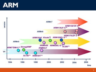
History ofARM
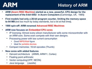
• ARM (Acorn RISC Machine) started as a new, powerful, CPU design for the
replacement of the 8-bit 6502 in Acorn Computers (Cambridge, UK, 1985)
• First models had only a 26-bit program counter, limiting the memory space
to 64 MB (not too much by today standards, but a lot at that time).
• 1990 spin-off: ARM renamed Advanced RISC Machines
• ARM now focuses on Embedded CPU cores
• IP licensing: Almost every silicon manufacturer sells some microcontroller with
an ARM core. Some even compete with their own designs.
• Processing power with low current consumption
• Good MIPS/Watt figure
• Ideal for portable devices
• Compact memories: 16-bit opcodes (Thumb)
• New cores with added features
• Harvard architecture (ARM9, ARM11, Cortex)
• Floating point arithmetic
• Vector computing(VFP, NEON)
• Java language (Jazelle)
3.
3
TM 3
Facts
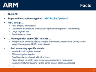
• 32-bitCPU
• 3-operand instructions (typical): ADD Rd,Rn,Operand2
• RISC design…
• Few, simple, instructions
• Load/store architecture (instructions operate on registers, not memory)
• Large register set
• Pipelined execution
• … Although with some CISC touches…
• Multiplication and Load/Store Multiple are complex instructions (many cycles
longer than regular, RISC, instructions)
• … And some very specific details
• No stack. Link register instead
• PC as a regular register
• Conditional execution of all instructions
• Flags altered or not by data processing instructions (selectable)
• Concurrent shifts/rotations (at the same time of other processing)
• …
7
TM 7
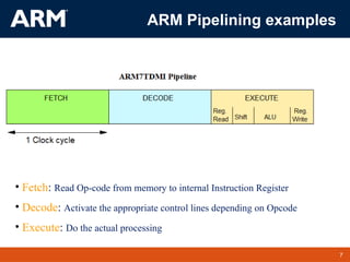
ARM Pipeliningexamples
• Fetch: Read Op-code from memory to internal Instruction Register
• Decode: Activate the appropriate control lines depending on Opcode
• Execute: Do the actual processing
8.
8
TM 8
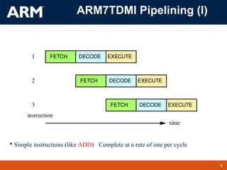
ARM7TDMI Pipelining(I)
FETCH DECODE EXECUTE
FETCH DECODE EXECUTE
FETCH DECODE EXECUTE
time
3
2
1
instruction
• Simple instructions (like ADD) Complete at a rate of one per cycle
11
TM 11
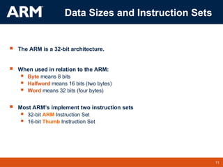
Data Sizesand Instruction Sets
The ARM is a 32-bit architecture.
When used in relation to the ARM:
Byte means 8 bits
Halfword means 16 bits (two bytes)
Word means 32 bits (four bytes)
Most ARM’s implement two instruction sets
32-bit ARM Instruction Set
16-bit Thumb Instruction Set
12.
12
TM 12
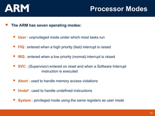
Processor Modes
The ARM has seven operating modes:
User : unprivileged mode under which most tasks run
FIQ : entered when a high priority (fast) interrupt is raised
IRQ : entered when a low priority (normal) interrupt is raised
SVC : (Supervisor) entered on reset and when a Software Interrupt
instruction is executed
Abort : used to handle memory access violations
Undef : used to handle undefined instructions
System : privileged mode using the same registers as user mode
13.
13
TM 13
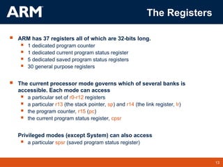
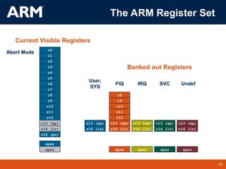
The Registers
ARM has 37 registers all of which are 32-bits long.
1 dedicated program counter
1 dedicated current program status register
5 dedicated saved program status registers
30 general purpose registers
The current processor mode governs which of several banks is
accessible. Each mode can access
a particular set of r0-r12 registers
a particular r13 (the stack pointer, sp) and r14 (the link register, lr)
the program counter, r15 (pc)
the current program status register, cpsr
Privileged modes (except System) can also access
a particular spsr (saved program status register)
15
TM 15
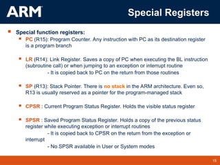
Special Registers
Special function registers:
PC (R15): Program Counter. Any instruction with PC as its destination register
is a program branch
LR (R14): Link Register. Saves a copy of PC when executing the BL instruction
(subroutine call) or when jumping to an exception or interrupt routine
- It is copied back to PC on the return from those routines
SP (R13): Stack Pointer. There is no stack in the ARM architecture. Even so,
R13 is usually reserved as a pointer for the program-managed stack
CPSR : Current Program Status Register. Holds the visible status register
SPSR : Saved Program Status Register. Holds a copy of the previous status
register while executing exception or interrupt routines
- It is copied back to CPSR on the return from the exception or
interrupt
- No SPSR available in User or System modes
16.
16
TM 16
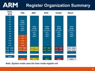
Register OrganizationSummary
User
mode
r0-r7,
r15,
and
cpsr
r8
r9
r10
r11
r12
r13 (sp)
r14 (lr)
spsr
FIQ
r8
r9
r10
r11
r12
r13 (sp)
r14 (lr)
r15 (pc)
cpsr
r0
r1
r2
r3
r4
r5
r6
r7
User,
SYS
r13 (sp)
r14 (lr)
spsr
IRQ
User
mode
r0-r12,
r15,
and
cpsr
r13 (sp)
r14 (lr)
spsr
Undef
User
mode
r0-r12,
r15,
and
cpsr
r13 (sp)
r14 (lr)
spsr
SVC
User
mode
r0-r12,
r15,
and
cpsr
r13 (sp)
r14 (lr)
spsr
Abort
User
mode
r0-r12,
r15,
and
cpsr
Note: System mode uses the User mode register set
17.
17
TM 17
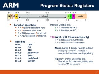
Program StatusRegisters
Condition code flags
N = Negative result from ALU
Z = Zero result from ALU
C = ALU operation Carried out
V = ALU operation oVerflowed
Interrupt Disable bits.
I = 1: Disables the IRQ.
F = 1: Disables the FIQ.
T Bit (Arch. with Thumb mode only)
T = 0: Processor in ARM state
T = 1: Processor in Thumb state
Never change T directly (use BX instead)
Changing T in CPSR will lead to
unexpected behavior due to pipelining
Tip: Don’t change undefined bits.
This allows for code compatibility with
newer ARM processors
Mode bits
10000 User
10001 FIQ
10010 IRQ
10011 Supervisor
10111 Abort
11011 Undefined
11111 System
I F T
N Z C V
31 28 27 24 23 16 15 7
8 6 5 4
mode
0
undefined
f x c
s
18.
18
TM 18
Whenthe processor is executing in ARM state:
All instructions are 32 bits wide
All instructions must be word aligned
Therefore the PC value is stored in bits [31:2] and bits [1:0] are zero
Due to pipelining, the PC points 8 bytes ahead of the current instruction, or 12
bytes ahead if current instruction includes a register-specified shift
When the processor is executing in Thumb state:
All instructions are 16 bits wide
All instructions must be halfword aligned
Therefore the PC value is stored in bits [31:1] and bit [0] is zero
Program Counter (R15)
19.
19
TM 19
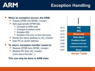
Vector Table
ExceptionHandling
When an exception occurs, the ARM:
Copies CPSR into SPSR_<mode>
Sets appropriate CPSR bits:
Changes to ARM state
Changes to related mode
Disables IRQ
Disables FIQ (only on fast interrupts)
Stores the return address in LR_<mode>
Sets PC to vector address
To return, exception handler needs to:
Restore CPSR from SPSR_<mode>
Restore PC from LR_<mode>
(more about this later…)
This can only be done in ARM state.
FIQ
IRQ
(Reserved)
Data Abort
Prefetch Abort
Software Interrupt
Undefined Instruction
Reset
0x1C
0x18
0x14
0x10
0x0C
0x08
0x04
0x00
21
TM 21
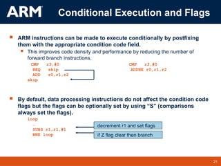
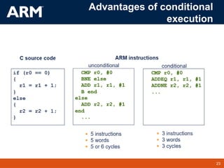
ARMinstructions can be made to execute conditionally by postfixing
them with the appropriate condition code field.
This improves code density and performance by reducing the number of
forward branch instructions.
CMP r3,#0 CMP r3,#0
BEQ skip ADDNE r0,r1,r2
ADD r0,r1,r2
skip
By default, data processing instructions do not affect the condition code
flags but the flags can be optionally set by using “S” (comparisons
always set the flags).
loop
…
SUBS r1,r1,#1
BNE loop if Z flag clear then branch
decrement r1 and set flags
Conditional Execution and Flags
22.
22
TM 22
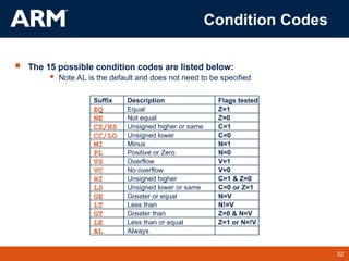
Condition Codes
Notequal
Unsigned higher or same
Unsigned lower
Minus
Equal
Overflow
No overflow
Unsigned higher
Unsigned lower or same
Positive or Zero
Less than
Greater than
Less than or equal
Always
Greater or equal
EQ
NE
CS/HS
CC/LO
PL
VS
HI
LS
GE
LT
GT
LE
AL
MI
VC
Suffix Description
Z=0
C=1
C=0
Z=1
Flags tested
N=1
N=0
V=1
V=0
C=1 & Z=0
C=0 or Z=1
N=V
N!=V
Z=0 & N=V
Z=1 or N=!V
The 15 possible condition codes are listed below:
Note AL is the default and does not need to be specified
24
TM 24
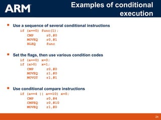
Examples ofconditional
execution
Use a sequence of several conditional instructions
if (a==0) func(1);
CMP r0,#0
MOVEQ r0,#1
BLEQ func
Set the flags, then use various condition codes
if (a==0) x=0;
if (a>0) x=1;
CMP r0,#0
MOVEQ r1,#0
MOVGT r1,#1
Use conditional compare instructions
if (a==4 || a==10) x=0;
CMP r0,#4
CMPEQ r0,#10
MOVEQ r1,#0
25.
25
TM 25
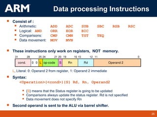
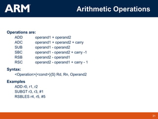
Data processingInstructions
Consist of :
Arithmetic: ADD ADC SUB SBC RSB RSC
Logical: AND ORR EOR BIC
Comparisons: CMP CMN TST TEQ
Data movement: MOV MVN
These instructions only work on registers, NOT memory.
L, Literal: 0: Operand 2 from register, 1: Operand 2 immediate
Syntax:
<Operation>{<cond>}{S} Rd, Rn, Operand2
{S} means that the Status register is going to be updated
Comparisons always update the status register. Rd is not specified
Data movement does not specify Rn
Second operand is sent to the ALU via barrel shifter.
31 28 25 24 20 16 15 12 11 0
21 19
0 Rd Operand 2
Rn
S
op-code
L
0
cond.
26.
26
TM 26
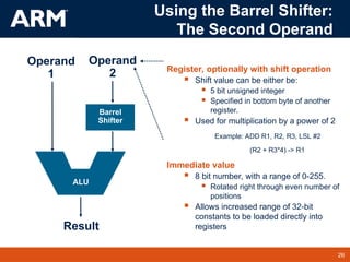
Register, optionallywith shift operation
Shift value can be either be:
5 bit unsigned integer
Specified in bottom byte of another
register.
Used for multiplication by a power of 2
Example: ADD R1, R2, R3, LSL #2
(R2 + R3*4) -> R1
Immediate value
8 bit number, with a range of 0-255.
Rotated right through even number of
positions
Allows increased range of 32-bit
constants to be loaded directly into
registers
Result
Operand
1
Barrel
Shifter
Operand
2
ALU
Using the Barrel Shifter:
The Second Operand
27.
27
TM 27
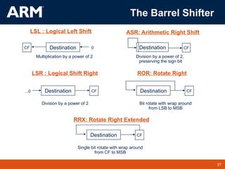
The BarrelShifter
Destination
CF 0 Destination CF
LSL : Logical Left Shift ASR: Arithmetic Right Shift
Multiplication by a power of 2 Division by a power of 2,
preserving the sign bit
Destination CF
...0 Destination CF
LSR : Logical Shift Right ROR: Rotate Right
Division by a power of 2 Bit rotate with wrap around
from LSB to MSB
Destination
RRX: Rotate Right Extended
Single bit rotate with wrap around
from CF to MSB
CF
28.
28
TM 28
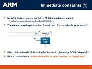
NoARM instruction can contain a 32 bit immediate constant
All ARM instructions are fixed as 32 bits long
The data processing instruction format has 12 bits available for operand2
4 bit rotate value (0-15) is multiplied by two to give range 0-30 in steps of 2
Rule to remember is “8-bits shifted by an even number of bit positions”.
0
7
11 8
immed_8
Shifter
ROR
rot
x2
Immediate constants (1)
29.
29
TM 29
Toallow larger constants to be loaded, the assembler offers a pseudo-
instruction:
LDR rd, =const (notice the “=“ sign)
This will either:
Produce a MOV or MVN instruction to generate the value (if possible).
or
Generate a LDR instruction with a PC-relative address to read the constant
from a literal pool (Constant data area embedded in the code).
For example
LDR r0,=0xFF => MOV r0,#0xFF
LDR r0,=0x55555555 => LDR r0,[PC,#Imm12]
…
…
DCD 0x55555555
This is the recommended way of loading constants into a register
Loading 32 bit constants
30.
30
TM 30
Data processinginstr. FLAGS
Flags are changed only if the S bit of the op-code is set:
Mnemonics ending with “s”, like “movs”, and comparisons: cmp, cmn, tst, teq
N and Z have the expected meaning for all instructions
N: bit 31 (sign) of the result
Z: set if result is zero
Logical instructions (AND, EOR, TST, TEQ, ORR, MOV, BIC, MVN)
V: unchanged
C: from barrel shifter if shift ≠ 0. Unchanged otherwise
Arithmetic instructions (SUB, RSB, ADD, ADC, SBC, RSC, CMP, CMN)
V: Signed overflow from ALU
C: Carry (bit 32 of result) from ALU
When PC is the destination register (exception return)
CPSR is copied from SPSR. This includes all the flags.
No change in user or system modes
Example: SUBS PC,LR,#4@ return from IRQ
32
TM 32
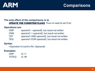
Comparisons
The onlyeffect of the comparisons is to
UPDATE THE CONDITION FLAGS
UPDATE THE CONDITION FLAGS. Thus no need to set S bit.
Operations are:
CMP operand1 - operand2, but result not written
CMN operand1 + operand2, but result not written
TST operand1 AND operand2, but result not written
TEQ operand1 EOR operand2, but result not written
Syntax:
<Operation>{<cond>} Rn, Operand2
Examples:
CMP r0, r1
TSTEQ r2, #5
33.
33
TM 33
Logical Operations
Operationsare:
AND operand1 AND operand2
EOR operand1 EOR operand2
ORR operand1 OR operand2
BIC operand1 AND NOT operand2 [ie bit clear]
Syntax:
<Operation>{<cond>}{S} Rd, Rn, Operand2
Examples:
AND r0, r1, r2
BICEQ r2, r3, #7
EORS r1,r3,r0
34.
34
TM 34
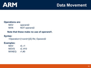
Data Movement
Operationsare:
MOV operand2
MVN NOT operand2
Note that these make no use of operand1.
Syntax:
<Operation>{<cond>}{S} Rd, Operand2
Examples:
MOV r0, r1
MOVS r2, #10
MVNEQ r1,#0
35.
35
TM 35
Multiply
Syntax:
MUL{<cond>}{S} Rd, Rm, Rs Rd = Rm * Rs
MLA{<cond>}{S} Rd,Rm,Rs,Rn Rd = (Rm * Rs) + Rn
[U|S]MULL{<cond>}{S} RdLo, RdHi, Rm, Rs RdHi,RdLo := Rm*Rs
[U|S]MLAL{<cond>}{S} RdLo, RdHi, Rm, Rs RdHi,RdLo:=(Rm*Rs)+RdHi,RdLo
Cycle time
Basic MUL instruction
2-5 cycles on ARM7TDMI
1-3 cycles on StrongARM/XScale
2 cycles on ARM9E/ARM102xE
+1 cycle for ARM9TDMI (over ARM7TDMI)
+1 cycle for accumulate (not on 9E though result delay is one cycle longer)
+1 cycle for “long”
Above are “general rules” - refer to the TRM for the core you are using for
the exact details
36.
36
TM 36
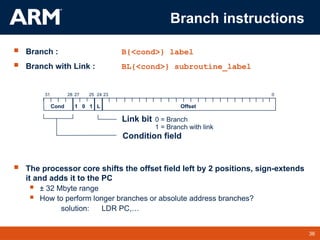
Branch: B{<cond>} label
Branch with Link : BL{<cond>} subroutine_label
The processor core shifts the offset field left by 2 positions, sign-extends
it and adds it to the PC
± 32 Mbyte range
How to perform longer branches or absolute address branches?
solution: LDR PC,…
28
31 24 0
Cond 1 0 1 L Offset
Condition field
Link bit 0 = Branch
1 = Branch with link
23
25
27
Branch instructions
37.
37
TM 37
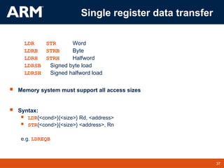
Single registerdata transfer
LDR STR Word
LDRB STRB Byte
LDRH STRH Halfword
LDRSB Signed byte load
LDRSH Signed halfword load
Memory system must support all access sizes
Syntax:
LDR{<cond>}{<size>} Rd, <address>
STR{<cond>}{<size>} <address>, Rn
e.g. LDREQB
38.
38
TM 38
Address accessed
Address accessed by LDR/STR is specified by a base register plus an
offset
For word and unsigned byte accesses, offset can be
An unsigned 12-bit immediate value (ie 0 - 4095 bytes).
LDR r0,[r1,#8]
A register, optionally shifted by an immediate value
LDR r0,[r1,r2]
LDR r0,[r1,r2,LSL#2]
This can be either added or subtracted from the base register:
LDR r0,[r1,#-8]
LDR r0,[r1,-r2]
LDR r0,[r1,-r2,LSL#2]
For halfword and signed halfword / byte, offset can be:
An unsigned 8 bit immediate value (ie 0-255 bytes).
A register (unshifted).
Choice of pre-indexed or post-indexed addressing
39.
39
TM 39
0x5
0x5
r1
0x200
Base
Register 0x200
r0
0x5
Source
Register
forSTR
Offset
12 0x20c
r1
0x200
Original
Base
Register
0x200
r0
0x5
Source
Register
for STR
Offset
12 0x20c
r1
0x20c
Updated
Base
Register
Base-update form (‘!’): STR r0,[r1,#12]!
Pre or Post Indexed Addressing?
Pre-indexed: STR r0,[r1,#12]
Post-indexed: STR r0,[r1],#12
Base register always updated
40.
40
TM 40
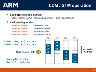
LDM /STM operation
Load/Store Multiple Syntax:
<LDM|STM>{<cond>}<addressing_mode> Rb{!}, <register list>
4 addressing modes:
LDMIA / STMIA increment after
LDMIB / STMIB increment before
LDMDA / STMDA decrement after
LDMDB / STMDB decrement before
IA
r1 Increasing
Address
r4
r0
r1
r4
r0
r1
r4
r0 r1
r4
r0
r10
IB DA DB
LDMxx r10, {r0,r1,r4}
STMxx r10, {r0,r1,r4}
Base Register (Rb)
Base-update possible:
LDM r10!,{r0-r6}
41.
41
TM 41
Atomic dataswap
Exchanges a word or byte between a register and a
memory location
This operation cannot be interrupted, not even by DMA
Main use: Operating System semaphores
Syntax:
SWP {<cond>} Rd, Rm, [Rn]
SWPB{<cond>} Rd, Rm, [Rn]
Rd=[Rn]; [Rn]=Rm (Rd and Rm can be the same)
Editor's Notes
#1 Programmers Model
The structure of the ARM architecture
How it has developed
Register set, modes and exceptions
The endian issue
#5 Programmers Model
The structure of the ARM architecture
How it has developed
Register set, modes and exceptions
The endian issue
#10 Programmers Model
The structure of the ARM architecture
How it has developed
Register set, modes and exceptions
The endian issue
#11 The cause of confusion here is the term “word” which will mean 16-bits to people with a 16-bit background.
In the ARM world 16-bits is a “halfword” as the architecture is a 32-bit one, whereas “word” means 32-bits.
Java bytecodes are 8-bit instructions designed to be architecture independent. Jazelle transparently executes most bytecodes in hardware and some in highly optimized ARM code. This is due to a tradeoff between hardware complexity (power consumption & silicon area) and speed.
#12 The Programmers Model can be split into two elements - first of all, the processor modes and secondly, the processor registers. So let’s start by looking at the modes.
Now the typical application will run in an unprivileged mode know as “User” mode, whereas the various exception types will be dealt with in one of the privileged modes : Fast Interrupt, Supervisor, Abort, Normal Interrupt and Undefined (and we will look at what causes each of the exceptions later on).
NB - spell out the word FIQ, otherwise you are saying something rude in German!
One question here is what is the difference between the privileged and unprivileged modes? Well in reality very little really - the ARM core has an output signal (nTRANS on ARM7TDMI, InTRANS, DnTRANS on 9, or encoded as part of HPROT or BPROT in AMBA) which indicates whether the current mode is privileged or unprivileged, and this can be used, for instance, by a memory controller to only allow IO access in a privileged mode. In addition some operations are only permitted in a privileged mode, such as directly changing the mode and enabling of interrupts.
All current ARM cores implement system mode (added in architecture v4). This is simply a privileged version of user mode. Important for re-entrant exceptions because no exceptions can cause system mode to be entered.
#13 The ARM architecture provides a total of 37 registers, all of which are 32-bits long. However these are arranged into several banks, with the accessible bank being governed by the current processor mode. We will see this in more detail in a couple of slides. In summary though, in each mode, the core can access:
a particular set of 13 general purpose registers (r0 - r12).
a particular r13 - which is typically used as a stack pointer. This will be a different r13 for each mode, so allowing each exception type to have its own stack.
a particular r14 - which is used as a link (or return address) register. Again this will be a different r14 for each mode.
r15 - whose only use is as the Program counter.
The CPSR (Current Program Status Register) - this stores additional information about the state of the processor:
And finally in privileged modes, a particular SPSR (Saved Program Status Register). This stores a copy of the previous CPSR value when an exception occurs. This combined with the link register allows exceptions to return without corrupting processor state.
#14 This animated slide shows the way that the banking of registers works. On the left the currently visible set of registers are shown for a particular mode.
On the right are the registers that are banked out whilst in that mode.
Each key press will switch mode:
user -> FIQ ->user -> IRQ -> user ->SVC -> User -> Undef -> User -> Abort and then back to user.
The following slide then shows this in a more static way that is more useful for reference
#15 The Programmers Model can be split into two elements - first of all, the processor modes and secondly, the processor registers. So let’s start by looking at the modes.
Now the typical application will run in an unprivileged mode know as “User” mode, whereas the various exception types will be dealt with in one of the privileged modes : Fast Interrupt, Supervisor, Abort, Normal Interrupt and Undefined (and we will look at what causes each of the exceptions later on).
NB - spell out the word FIQ, otherwise you are saying something rude in German!
One question here is what is the difference between the privileged and unprivileged modes? Well in reality very little really - the ARM core has an output signal (nTRANS on ARM7TDMI, InTRANS, DnTRANS on 9, or encoded as part of HPROT or BPROT in AMBA) which indicates whether the current mode is privileged or unprivileged, and this can be used, for instance, by a memory controller to only allow IO access in a privileged mode. In addition some operations are only permitted in a privileged mode, such as directly changing the mode and enabling of interrupts.
All current ARM cores implement system mode (added in architecture v4). This is simply a privileged version of user mode. Important for re-entrant exceptions because no exceptions can cause system mode to be entered.
#16 This slide shows the registers visible in each mode - basically in a more static fashion than the previous animated slide that is more useful for reference.
The main point to state here is the splitting of the registers in Thumb state into Low and High registers.
ARM register banking is the minimum necessary for fast handling of overlapping exceptions of different types (e.g. ABORT during SWI during IRQ). For nested exceptions of the same type (e.g. re-entrant interrupts) some additional pushing of registers to the stack is required.
#17 Green psr bits are only in certain versions of the ARM architecture
ALU status flags (set if "S" bit set, implied in Thumb state).
Sticky overflow flag (Q flag) is set either when
saturation occurs during QADD, QDADD, QSUB or QDSUB, or
the result of SMLAxy or SMLAWx overflows 32-bits
Once flag has been set can not be modified by one of the above instructions and must write to CPSR using MSR instruction to cleared
PSRs split into four 8-bit fields that can be individually written:
Control (c) bits 0-7
Extension (x) bits 8-15 Reserved for future use
Status (s) bits 16-23 Reserved for future use
Flags (f) bits 24-31
Bits that are reserved for future use should not be modified by current software. Typically, a read-modify-write strategy should be used to update the value of a status register to ensure future compatibility. Note that the T/J bits in the CPSR should never be changed directly by writing to the PSR (use the BX/BXJ instruction to change state instead).
However, in cases where the processor state is known in advance (e.g. on reset, following an interrupt, or some other exception), an immediate value may be written directly into the status registers, to change only specific bits (e.g. to change mode).
New ARM V6 bits now shown.
#18 ARM is designed to efficiently access memory using a single memory access cycle. So word accesses must be on a word address boundary, halfword accesses must be on a halfword address boundary. This includes instruction fetches.
Point out that strictly, the bottom bits of the PC simply do not exist within the ARM core - hence they are ‘undefined’. Memory system must ignore these for instruction fetches.
In Jazelle state, the processor doesn’t perform 8-bit fetches from memory. Instead it does aligned 32-bit fetches (4-byte prefetching) which is more efficient. Note we don’t mention the PC in Jazelle state because the ‘Jazelle PC’ is actually stored in r14 - this is technical detail that is not relevant as it is completely hidden by the Jazelle support code.
#19 Exception handling on the ARM is controlled through the use of an area of memory called the vector table. This lives (normally) at the bottom of the memory map from 0x0 to 0x1c. Within this table one word is allocated to each of the various exception types.
This word will contain some form of ARM instruction that should perform a branch. It does not contain an address.
Reset - executed on power on
Undef - when an invalid instruction reaches the execute stage of the pipeline
SWI - when a software interrupt instruction is executed
Prefetch - when an instruction is fetched from memory that is invalid for some reason, if it reaches the execute stage then this exception is taken
Data - if a load/store instruction tries to access an invalid memory location, then this exception is taken
IRQ - normal interrupt
FIQ - fast interrupt
When one of these exceptions is taken, the ARM goes through a low-overhead sequence of actions in order to invoke the appropriate exception handler. The current instruction is always allowed to complete (except in case of Reset).
IRQ is disabled on entry to all exceptions; FIQ is also disabled on entry to Reset and FIQ.
#20 Instruction Sets
Overview of the features of the ARM instruction set
The coprocessor mechanism
Overview of Thumb - Why it was designed and the benefits it gives.
#21 Unusual but powerful feature of the ARM instruction set. Other architectures normally only have conditional branches.
Some recently-added ARM instructions (in v5T and v5TE) are not conditional (e.g. v5T BLX offset)
Core compares condition field in instruction against NZCV flags to determine if instruction should be executed.
#22 Condition codes are simply a way of testing the ALU status flags.
#24 Sequence of conditional instructions:
- no instruction must reset cond code flags
- BL corrupts flags so must be last
- limit sequence to max 3 or so instrs
Can use different condition codes. Give if then else example. Note GCD practical coming later.
Conditional compare
- resets condition code when executed
- compiler will make use of this
- can be difficult for a human to understand!
Not just for compare, using data processing with condition code and S bit is useful in some circumstances.
LDM/LDR instruction cannot set flags due to datapath issues (data comes back only at the very end of the cycle, so there is no opportunity to perform a comparison and set the status flags).
#25 BIC bit clear
ORR bit set
AND bit mask
EOR bit invert
Comparisons produce no results - just set condition codes.
CMP like SUB
CMN like ADD (subtract of a negative number is the same as add)
TST like AND
TEQ like EOR (eor of identical numbers gives result of zero)
Generally single-cycle execution (except write to PC and register-controlled shift). Mention ARM NOP & Thumb NOP.
Explain RSB and RSC which do subtract in other order (e.g. y-x not x-y)
Does not include multiply (separate instr format). No divide - compiler uses run-time library or barrel shifter to perform division.
Can combine “S” bit with conditional execution, e.g.
ADDEQS r0, r1, r2
#26 Mention A bus and B bus on 7TDMI core.
Give examples:
ADD r0, r1, r2
ADD r0, r1, r2, LSL#7
ADD r0, r1, r2, LSL r3
ADD r0, r1, #0x4E
#27 Rotate left can be implemented as rotate right (32-number), e.g. rotate left of 10 is performed using rotate right of 22.
RRX shifts by 1 bit position, of a 33 bit amount (includes carry flag). Very specialized application (e.g. encryption algorithms). Cannot be generated by C compiler. We have used it for 64/64 bit divide. RRX allows you to shift multiprecision values right by one efficiently. Also used in ARM’s MPEG code in a very tricky piece of code.
ANSI C does not have a rotate operation (it only has “<<“ and “>>” which are the equivalent of LSL, LSR and ASR). However the ARM compiler recognizes rotate type expresssions and optimizes these to use ROR, e.g.
int f(unsigned int a)
{
return (a << 10) | (a >>22) ;
}
=> MOV a1,a1,ROR #22
Carry flag set out of the shifter for *logical* data processing operations
#28 Could have used 12 bits directly for immediate value - this would allow 0-4095. But this does not allow any large numbers, which are useful for:
base address of memory devices in target system
large, but simple hex constants (0x10000)
Research has shown there is a need for a large range of small numbers (frequently needed) but also some large numbers. 50% of all constants lie between the range -15 and +15 and 90% lie in the range -511 and +511. Will vary depending on the application.
ROR #n is confusing… but can be considered as ROL #32-n
Opcode 0xe3a004ff = MOV r0, #0xff, 8
Core rotates 0xff right by 4 pairs of bits
=> MOV r0, #0xff000000
#29
Literal pools
These are constant data areas embedded in the code at the end of assembler modules, and at other locations if specified by the user using LTORG. Data value must not be executed (will probably be an undefined instruction), assembly programmer must ensure this by placing LTORG at an appropriate location. ARM C compilers will handle placement of literal pools automatically.
#35 Variable number of cycles for some processors which implement ‘early termination’. The multiply is faster for smaller values in Rs.
ARM7TDMI and ARM9TDMI use 8-bit Booth’s algorithm which takes 1 cycle for each byte in Rs. Terminates when rest of Rs is all zeros or all ones.
MUL/MLA don’t need signed/unsigned specified - because they return the low 32-bit of the result which is the same whatever the sign of the arguments.
Cycle information is general and specific cores have some specific variations from this, specifically with respect to result delays where accumulation is involved. Refer to TRM for exact details if required.
XScale and StrongARM have a split pipeline with multiple execution units - so can issue multiplies in 1 or 2 cycles and continue with following instructions, assuming no resource or result dependencies.
XScale can issue MUL/MLA/MULL in one cycle (MLAL requires 2 cycles), providing multiplier is not already in use. Cycle timing is dependent on result latency - the core will stall if an instruction tries to use the result before multiplier has completed.
Note that there is no form of the multiply instruction which has an immediate constant operand - registers only.
For the interested student - C flag is unpredictable if S is set in architectures prior to V5.
MULS/MLAS always take 4 cycles; MULLS, MLALS always take 5.
#36 PC-relative to allow position independent code, and allows restricted branch range to jump to nearby addresses.
How to access full 32-bit address space? Can set up LR manually if needed, then load into PC
MOV lr, pc
LDR pc, =dest
ADS linker will automatically generate long branch veneers for branches beyond 32Mb range.
#37 Point out destination (reg) first for LDR, but destination (mem) last for STR. Different to Motorola, but it keeps the instruction mnemonic format consistent. Always have register loaded/stored first, then address accessed second
Size specifier comes out on MAS (memory access size) signal. Important that memory supports full range of accesses - especially important for writes where only the specified size should be written.
Special types of sign extended load - this is needed because ARM registers only hold 32-bit values. Draw diagram. No need for special store instructions though.
Instruction cycle timing:
STR LDR
7TDMI 2 cycles 3 cycles
9TDMI 1 cycle 1 cycle - interlock if used in next cycle
StrongARM1 1 cycle 1 cycle - interlock if used in next cycle
Xscale 1 cycle 1 cycle - interlock if used in next 2 cycles
Note size specifier comes after condition code.
Link: <address> explained on next slide.
Note that load/store instructions never set condition codes.
#38 Halfword access and signed halfword/byte accesses were added to the architecture in v4T, this is the reason the offset field is not as flexible as the normal word/byte load/store - not a problem because these accesses are less common.
Link: diagram on next slide
#39 “!” indicates “writeback” i.e. the base register is to be updated after the instruction.
No “!” for post-indexed because post-increment of base register always happens (otherwise the offset field would not be used at all).
Give C example:
int *ptr;
x = *ptr++;
Compiles to a single instruction:
LDR r0, [r1], #4
#40 Always lowest register first.
Always ascending memory address order.
Uses sequential cycles to take advantage of faster access.
‘addressing_mode’ just determines whether up/down with respect to the base pointer and if value at base pointer address is accessed or skipped. It isn’t possible to add any offset to the base pointer.
Note address and registers loaded/stored are the other way around compared with LDM/STM.
Note the base pointer is not loaded or stored, unless it is in the reg list.
![Address Register
REGISTER
BANK
PC
Address
Incrementer
SHIFT
Multiplier
Write Data Reg.
translator
D[31:0]
INSTRUCCTION
DECODER
Control
Lines
ARM
Thumb to
Instruction Reg.
Read Data Reg.
B
bus
A
bus
ALU
bus
PC
bus
A[31:0]
A.L.U.
ARM7TDMI
Block Diagram](https://image.slidesharecdn.com/arm-introduction-250715091638-1e160ae1/85/AdvancedRiscMachineryss-INTRODUCTION-ppt-6-320.jpg)
![18
TM 18
When the processor is executing in ARM state:
All instructions are 32 bits wide
All instructions must be word aligned
Therefore the PC value is stored in bits [31:2] and bits [1:0] are zero
Due to pipelining, the PC points 8 bytes ahead of the current instruction, or 12
bytes ahead if current instruction includes a register-specified shift
When the processor is executing in Thumb state:
All instructions are 16 bits wide
All instructions must be halfword aligned
Therefore the PC value is stored in bits [31:1] and bit [0] is zero
Program Counter (R15)](https://image.slidesharecdn.com/arm-introduction-250715091638-1e160ae1/85/AdvancedRiscMachineryss-INTRODUCTION-ppt-18-320.jpg)
![29
TM 29
To allow larger constants to be loaded, the assembler offers a pseudo-
instruction:
LDR rd, =const (notice the “=“ sign)
This will either:
Produce a MOV or MVN instruction to generate the value (if possible).
or
Generate a LDR instruction with a PC-relative address to read the constant
from a literal pool (Constant data area embedded in the code).
For example
LDR r0,=0xFF => MOV r0,#0xFF
LDR r0,=0x55555555 => LDR r0,[PC,#Imm12]
…
…
DCD 0x55555555
This is the recommended way of loading constants into a register
Loading 32 bit constants](https://image.slidesharecdn.com/arm-introduction-250715091638-1e160ae1/85/AdvancedRiscMachineryss-INTRODUCTION-ppt-29-320.jpg)
![33
TM 33
Logical Operations
Operations are:
AND operand1 AND operand2
EOR operand1 EOR operand2
ORR operand1 OR operand2
BIC operand1 AND NOT operand2 [ie bit clear]
Syntax:
<Operation>{<cond>}{S} Rd, Rn, Operand2
Examples:
AND r0, r1, r2
BICEQ r2, r3, #7
EORS r1,r3,r0](https://image.slidesharecdn.com/arm-introduction-250715091638-1e160ae1/85/AdvancedRiscMachineryss-INTRODUCTION-ppt-33-320.jpg)
![35
TM 35
Multiply
Syntax:
MUL{<cond>}{S} Rd, Rm, Rs Rd = Rm * Rs
MLA{<cond>}{S} Rd,Rm,Rs,Rn Rd = (Rm * Rs) + Rn
[U|S]MULL{<cond>}{S} RdLo, RdHi, Rm, Rs RdHi,RdLo := Rm*Rs
[U|S]MLAL{<cond>}{S} RdLo, RdHi, Rm, Rs RdHi,RdLo:=(Rm*Rs)+RdHi,RdLo
Cycle time
Basic MUL instruction
2-5 cycles on ARM7TDMI
1-3 cycles on StrongARM/XScale
2 cycles on ARM9E/ARM102xE
+1 cycle for ARM9TDMI (over ARM7TDMI)
+1 cycle for accumulate (not on 9E though result delay is one cycle longer)
+1 cycle for “long”
Above are “general rules” - refer to the TRM for the core you are using for
the exact details](https://image.slidesharecdn.com/arm-introduction-250715091638-1e160ae1/85/AdvancedRiscMachineryss-INTRODUCTION-ppt-35-320.jpg)
![38
TM 38
Address accessed
Address accessed by LDR/STR is specified by a base register plus an
offset
For word and unsigned byte accesses, offset can be
An unsigned 12-bit immediate value (ie 0 - 4095 bytes).
LDR r0,[r1,#8]
A register, optionally shifted by an immediate value
LDR r0,[r1,r2]
LDR r0,[r1,r2,LSL#2]
This can be either added or subtracted from the base register:
LDR r0,[r1,#-8]
LDR r0,[r1,-r2]
LDR r0,[r1,-r2,LSL#2]
For halfword and signed halfword / byte, offset can be:
An unsigned 8 bit immediate value (ie 0-255 bytes).
A register (unshifted).
Choice of pre-indexed or post-indexed addressing](https://image.slidesharecdn.com/arm-introduction-250715091638-1e160ae1/85/AdvancedRiscMachineryss-INTRODUCTION-ppt-38-320.jpg)
![39
TM 39
0x5
0x5
r1
0x200
Base
Register 0x200
r0
0x5
Source
Register
for STR
Offset
12 0x20c
r1
0x200
Original
Base
Register
0x200
r0
0x5
Source
Register
for STR
Offset
12 0x20c
r1
0x20c
Updated
Base
Register
Base-update form (‘!’): STR r0,[r1,#12]!
Pre or Post Indexed Addressing?
Pre-indexed: STR r0,[r1,#12]
Post-indexed: STR r0,[r1],#12
Base register always updated](https://image.slidesharecdn.com/arm-introduction-250715091638-1e160ae1/85/AdvancedRiscMachineryss-INTRODUCTION-ppt-39-320.jpg)
![41
TM 41
Atomic data swap
Exchanges a word or byte between a register and a
memory location
This operation cannot be interrupted, not even by DMA
Main use: Operating System semaphores
Syntax:
SWP {<cond>} Rd, Rm, [Rn]
SWPB{<cond>} Rd, Rm, [Rn]
Rd=[Rn]; [Rn]=Rm (Rd and Rm can be the same)](https://image.slidesharecdn.com/arm-introduction-250715091638-1e160ae1/85/AdvancedRiscMachineryss-INTRODUCTION-ppt-41-320.jpg)