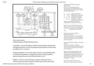
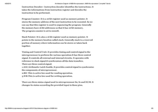
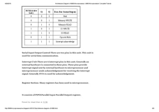
4/26/2015 Architecture Diagram of 8085 Microprocessor | 8085 Microprocessor Complete Tutorial
http://8085microprocessor4u.blogspot.in/2012/12/architecture­diagram­of­8085.html 1/9
Bloggertemplates
PopularPosts
Architecture Diagram of 8085
Microprocessor
This is the functional block diagram of
the 8085 Microprocessor. This is the
function al Block Diagram of 8085
Microprocessor. Acum...
Pin Diagram of 8085 Microprocessor
with Description
8085 is a general purpose microprocessor
having 40 pins and works on single
power supply. To study the pin diagram
we group  the signals ...
All Addressing Modes in 8085
Microprocessor With Example
Addressing Modes in 8085 There are five
addressing modes in 8085. 1. Immediate
Addressing Mode: ­ An immediate is
transferred directly ...
8085MicroprocessorCompleteTutorial type your search and hit enter
Friday, 7 December 2012
Architecture Diagram of 8085
Microprocessor
This is the functional block diagram of the 8085 Microprocessor.
4/26/2015 Architecture Diagram of 8085 Microprocessor | 8085 Microprocessor Complete Tutorial
http://8085microprocessor4u.blogspot.in/2012/12/architecture­diagram­of­8085.html 2/9
Applications Of Microprocessor in
General Life
There are a lot of applications of
Microprocessor in general life.Some of
the applications are given below: Mobile
Phones Digital Watch...
Difference Between
Address Bus vs Data Bus
of 8085 Microprocessor
According to computer
architecture, a bus is
defined as a system that
transfers data between hardware
components of a computer or betwee...
Bus Structure Of 8085 Microprocessor
There are three buses in Microprocessor:
1.Address Bus 2.Data Bus 3.Control Bus  
                    1.Address Bus:­Genearlly,
Mic...
Hardware Interrupts in 8085......
(Interrupts Contd)........
Hardware Interrupt:­ As i have already
discussed that there are 6 interrupt pins
in the microprocessor used as Hardware
Interrrupts given...
Software Interrupts in 8085.....(Interrupt
Contd..)
Software Interrupts:­ A software
interrupts is a particular instructions that
can be inserted into the desired location
in the rpogram. T...
Memory Interfacing Using RAM and
ROM both with 8085 Microprocessor
Interfacing RAM and ROM both at a time
with 8085: Here ROM with 32 kb and
RAM with 64kb has been used. 32kb =
32768bytes   is equal ...
Interrupts in 8085 Microprocessor
First of all i want to discuss that what is
This is the function
al Block Diagram of 8085 Microprocessor.
Acumulator:­It is a 8­bit register which is used to perform airthmetical
and logical operation. It stores the output of any operation. It also works
as registers for i/o accesses.
Temporary Register:­It is a 8­bit register which is used to hold the data
on which the acumulator is computing operation. It is also called as
operand register because it provides operands to ALU.
Registers:­These are general purposes registers. Microprocessor
consists 6 general purpose registers of 8­bit each named as B,C,D,E,H
4/26/2015 Architecture Diagram of 8085 Microprocessor | 8085 Microprocessor Complete Tutorial
http://8085microprocessor4u.blogspot.in/2012/12/architecture­diagram­of­8085.html 3/9
Interrupt??????? Interrupt is a
mechanism by which an I/O or an
instruction can suspend the ...
Blogroll
Blogarchive
►  2015 (1)
▼  2012 (16)
▼  December (16)
Hardware Interrupts in 8085......
(Interrupts Contd...
Software Interrupts in 8085.....
(Interrupt Contd.....
Interrupts in 8085 Microprocessor
Memory Interfacing Using RAM
and ROM both with 808...
Memory Interfacing in 8085
Microprocessor
Representation of signals in Timing
Diagram Of 808...
Some Short Questions Self Test
How to Demultiplex Address and
Data Bus
All Addressing Modes in 8085
Microprocessor With E...
Pin Diagram of 8085
Microprocessor with Descriptio...
Microcomputers and
Microprocessor
Difference Between Address Bus vs
Data Bus of 808...
Bus Structure Of 8085
and L.   Generally theses registers are not used for storing the data
permanently. It carries the 8­bits data. These are used only during the
execution of the instructions.
These registers can also be used to carry the 16 bits data by making the
pair of 2 registers. The valid register pairs available are BC,DE HL. We
can not use other pairs except BC,DEand HL. These registers are
programmed by user.
ALU:­ALU performs the airthmetic operations and logical operation.
Flag Registers:­It consists of 5 flip flop which changes its status
according to the result stored in an accumulator. It is also known as
status registers. It is connected to the ALU.
There are five flip­flops in the flag register are as follows:
1.Sign(S)
2.zero(z)
3.Auxiliary carry(AC)
4/26/2015 Architecture Diagram of 8085 Microprocessor | 8085 Microprocessor Complete Tutorial
http://8085microprocessor4u.blogspot.in/2012/12/architecture­diagram­of­8085.html 4/9
Microprocessor
Architecture Diagram of 8085
Microprocessor
Applications Of Microprocessor in
General Life
Introduction to Microprocessor
LatestTweets
...searching twitter...
4.Parity(P)
5.Carry(C)
The bit position of the flip flop in flag register is:
                 
                              
All of the three flip flop set and reset according to the stored result in the
accumulator.
1.Sign­ If D7 of the result is 1 then sign flag is set otherwise reset. As we
know that a number on the D7 always desides the sign of the number.
if D7 is 1: the number is negative.
if D7 is 0: the number is positive.
2.Zeros(Z)­If the result stored in an accumulator is zero then this flip
flop is set otherwise it is reset.
3.Auxiliary carry(AC)­If any carry goes from D3 to D4 in the output then
it is set otherwise it is reset.
4.Parity(P)­If the no of 1's is even in the output stored in the
accumulator then it is set otherwise it is reset for the odd.
5.Carry(C)­If the result stored in an accumulator generates a carry in its
final output then it is set otherwise it is reset.
Instruction registers(IR):­It is a 8­bit register. When an instruction is
fetched from memory then it is stored in this register.
4/26/2015 Architecture Diagram of 8085 Microprocessor | 8085 Microprocessor Complete Tutorial
http://8085microprocessor4u.blogspot.in/2012/12/architecture­diagram­of­8085.html 5/9
Instruction Decoder:­ Instruction decoder identifies the instructions. It
takes the informations from instruction register and decodes the
instruction to be performed.
Program Counter:­It is a 16 bit register used as memory pointer. It
stores the memory address of the next instruction to be executed. So we
can say that this register is used to sequencing the program. Generally
the memory have 16 bit addresses so that it has 16 bit memory.
The program counter is set to 0000H.
Stack Pointer:­It is also a 16 bit register used as memory pointer. It
points to the memory location called stack. Generally stack is a reserved
portion of memory where information can be stores or taken back
together.
Timing and Control Unit:­It provides timing and control signal to the
microprocessor to perform the various operation.It has three control
signal. It controls all external and internal circuits. It operates with
reference to clock signal.It synchronizes all the data transfers.
There are three control signal:
1.ALE­Airthmetic Latch Enable, It provides control signal to synchronize
the components of microprocessor.
2.RD­ This is active low used for reading operation.
3.WR­This is active low used for writing operation.
There are three status signal used in microprocessor S0, S1 and IO/M. It
changes its status according the provided input to these pins.
                                 
4/26/2015 Architecture Diagram of 8085 Microprocessor | 8085 Microprocessor Complete Tutorial
http://8085microprocessor4u.blogspot.in/2012/12/architecture­diagram­of­8085.html 6/9
Serial Input Output Control­There are two pins in this unit. This unit is
used for serial data communication.
Interrupt Unit­There are 6 interrupt pins in this unit. Generally an
external hardware is connected to these pins. These pins provide
interrupt signal sent by external hardware to microprocessor and
microprocessor sends acknowledgement for receiving the interrupt
signal. Generally INTA is used for acknowledgement. 
Register Section:­Many registers has been used in microprocessor. 
                    
It consists of PIPO(Parallel Input Parallel Output) register.
Posted by imaad khan at 11:54
4/26/2015 Architecture Diagram of 8085 Microprocessor | 8085 Microprocessor Complete Tutorial
http://8085microprocessor4u.blogspot.in/2012/12/architecture­diagram­of­8085.html 7/9
8 comments:
aman srivastava said...
Very nice description. Well done n a grt thanxxxx.
Aman Srivastava. 
iet lucknow
25 April 2014 at 12:44
พงษ์พันธุ์ โปรณะ said...
Where's example code ? Sent to phongphanp@yahoo.com , please !!!
6 July 2014 at 08:23
Raktim Laha said...
thank for sharing the nice post.
19 September 2014 at 04:02
Reena John said...
very nice description......... thank you
6 February 2015 at 09:40
rao harshitha said...
thankyou so much for your valuable notes its lucent
20 February 2015 at 07:50
Shalin Siriwaradhana said...
What is the diagram software used to create these diagrams? Is it a online
diagram tool , looking for one that works for Ubuntu.
9 April 2015 at 04:03
Abhishek Kumar said...
thnkq for sharing notes..@abhishek from araah
4/26/2015 Architecture Diagram of 8085 Microprocessor | 8085 Microprocessor Complete Tutorial
http://8085microprocessor4u.blogspot.in/2012/12/architecture­diagram­of­8085.html 8/9
Newer Post Older PostHome
Post a Comment
Enter your comment...
Comment as:  Google Account
Publish
  Preview
 
15 April 2015 at 09:33
Abhishek Kumar said...
thnkq for sharing notes..@abhishek from araah
15 April 2015 at 09:49
4/26/2015 Architecture Diagram of 8085 Microprocessor | 8085 Microprocessor Complete Tutorial
http://8085microprocessor4u.blogspot.in/2012/12/architecture­diagram­of­8085.html 9/9
Theme by Site5. 
Experts in Web Hosting.
© Copyright 2011 Diary/Notebook Theme by Site5.com. All Rights Reserved. by TNB
;

Architecture diagram of 8085 microprocessor 8085 microprocessor complete tutorial