This document describes three examples of analog signal conditioning circuits:
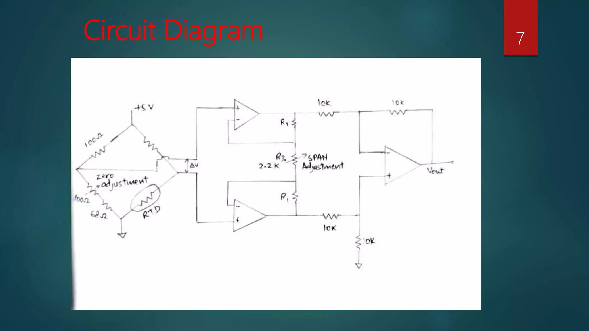
1. An RTD temperature sensor ranging from 0-100°C is converted to an output voltage of 0-5V using a Wheatstone bridge circuit and instrumentation amplifier. Variable resistors provide zero and span adjustments.
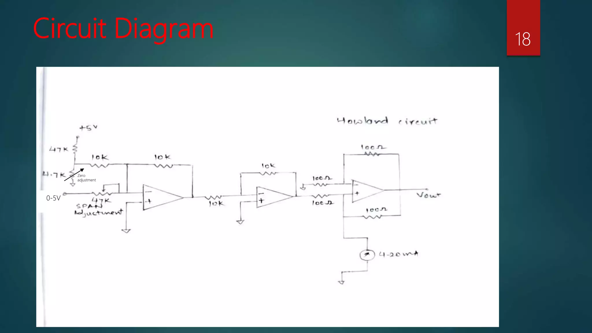
2. A current input of 4-20mA is converted to a voltage output of 0-5V using a resistor-based circuit. Variable resistors again provide zero and span adjustments.
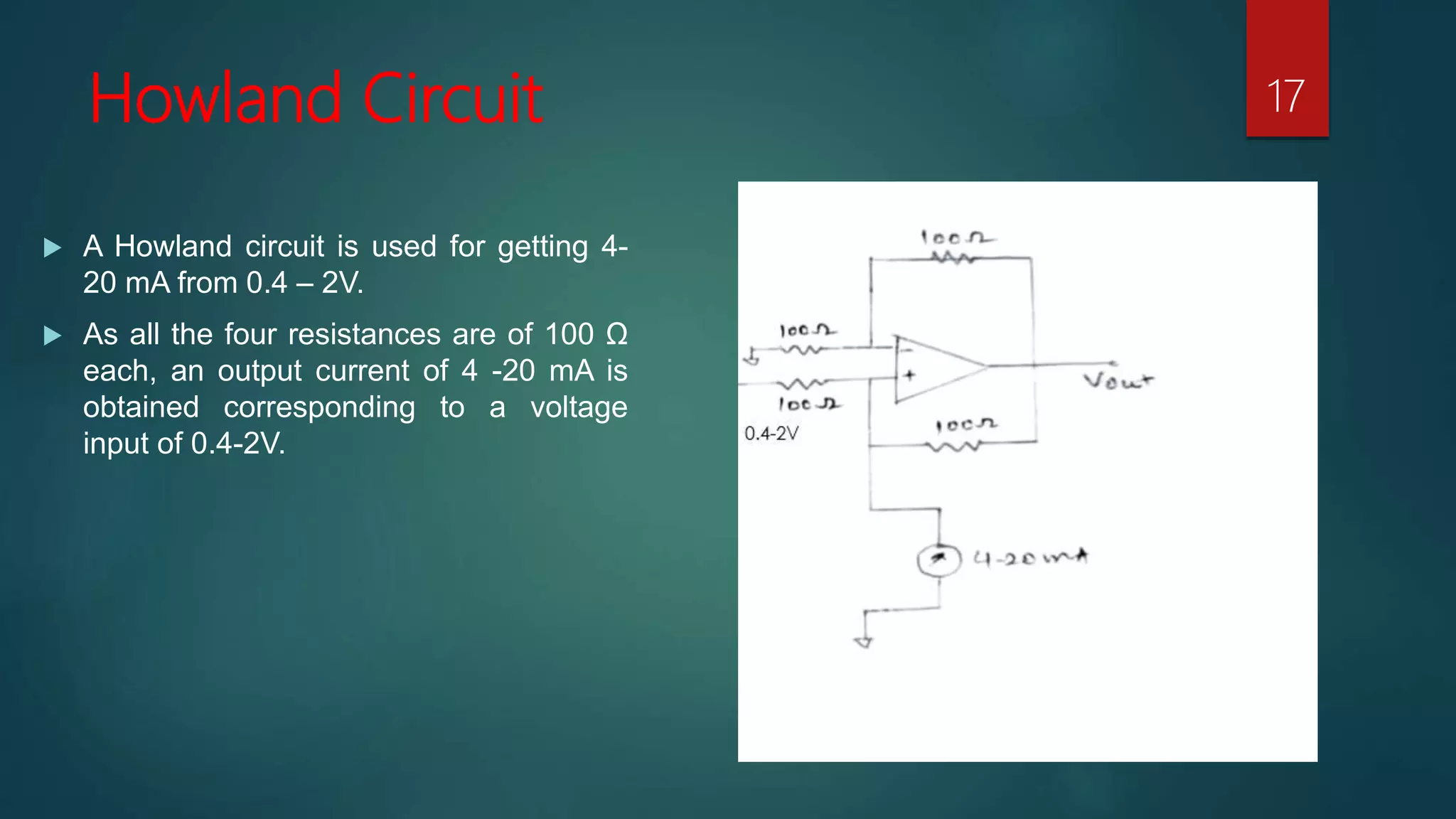
3. A voltage input of 0-5V is converted to a current output of 4-20mA using a Howland circuit. Variable resistors provide zero and span adjustments.

![Solution
RTD Pt-100 has a resistance of 100 Ω at 00C
At 1000C, its resistance will be R100 = R0 [1+αt] = 100[1+0.0039 x 100] = 139 Ω
α is the temperature coefficient of resistance whose value is 0.0039/0C for
platinum.
The RTD is connected in a Wheatstone Bridge circuit which is excited by +5V
DC.
3](https://image.slidesharecdn.com/analogsignalconditioning-210511053351/75/Analog-signal-conditioning-3-2048.jpg)

![Solution Contd…
The bridge unbalance voltage at 00C, ΔV = 0V
At 1000C, ΔV = [(5 x 139) / (139+100)] – [(5 x 100) / (100+100)] = 0.4V
Hence, the temperature variation of 00C – 1000C is converted into 0 – 0.4 V
This is further converted into 0 – 5V by the instrumentation amplifier.
Therefore, the gain of the amplifier will be (5 – 0) / (0.4 – 0) = 12.5
5](https://image.slidesharecdn.com/analogsignalconditioning-210511053351/75/Analog-signal-conditioning-5-2048.jpg)


![Sensor Technology Lecture 6 [Autosaved].pptx](https://cdn.slidesharecdn.com/ss_thumbnails/lecture6autosaved-250626060615-a31db175-thumbnail.jpg?width=640&height=640&fit=bounds)