The document discusses the structure and characteristics of semiconductor p-n junction diodes. It begins by explaining the atomic structure of semiconductors and how dopants are used to create an excess or deficiency of charge carriers, known as n-type and p-type materials. When a p-type and n-type semiconductor are joined, charge carriers diffuse across the junction to form a depletion region. Under forward bias, the depletion region narrows, allowing current to flow. Under reverse bias, the depletion region widens, blocking most current flow. The voltage-current characteristics of a p-n junction diode under forward and reverse bias are described.
BASIC ELECTRONICS
Electronics is a branch of physics that deals with the emission and effects of electrons in materials.
Or
Is a branch of science dealing with the study and development of circuit involving semi conductors, logic gates and other electrical components like resistors, capacitors and inductors.
The above document throws light on the fundamentals of semiconducting materials that includes the formation of bonds, distribution of carriers, p-type and n-type semiconductors, position of Fermi energy in intrinsic and extrinsic semiconductors, direct and indirect bandgap semiconductors and their applications, carrier concentration, the electric conductivity of semiconductors and Hall effect theory and applications.
Theoretically investigate the nature of direct band gap of novel materialsUCP
DIRECT BAND GAP:
In the direct band gap band to band recombination and generation occur.
Band to band recombination:
In band-to-band recombination electron from conduction band directly come back to valance band (in valance band holes are present which are the deficiency of electrons which are form when electrons leave valance band and go to conduction band) The electrons and holes annihilate each other the excess energy release during this process in the form of light called photon or in the form of thermal energy.
Band to band recombination is called direct band recombination.
Band to band generation:
In band-to-band generation electron is excited directly from valance band in to the conduction band after absorbing the thermal energy or photon(light) as shown in fig. given bellow.
If the thermal energy is absorbed this process is called thermal generation
If the light is absorbed this process is called photo generation
Momentum consideration in direct band:
In the EK plot K is the parameter proportional to momentum of electron.
GaAs is a notable member of direct band semiconductor
Photons, being massless entities carry the little momentum.
In direct band-band recombination K-value of electron’s and holes are all bounced k=o.as shown in figure given bellow, the little change in momentum is required for the recombination process to proceed.
For conservation of energy and momentum simply the photon is emitted
Energy and momentum have parabolic shape
Welcome to TechSoup New Member Orientation and Q&A (May 2024).pdfTechSoup
In this webinar you will learn how your organization can access TechSoup's wide variety of product discount and donation programs. From hardware to software, we'll give you a tour of the tools available to help your nonprofit with productivity, collaboration, financial management, donor tracking, security, and more.
Read| The latest issue of The Challenger is here! We are thrilled to announce that our school paper has qualified for the NATIONAL SCHOOLS PRESS CONFERENCE (NSPC) 2024. Thank you for your unwavering support and trust. Dive into the stories that made us stand out!
We all have good and bad thoughts from time to time and situation to situation. We are bombarded daily with spiraling thoughts(both negative and positive) creating all-consuming feel , making us difficult to manage with associated suffering. Good thoughts are like our Mob Signal (Positive thought) amidst noise(negative thought) in the atmosphere. Negative thoughts like noise outweigh positive thoughts. These thoughts often create unwanted confusion, trouble, stress and frustration in our mind as well as chaos in our physical world. Negative thoughts are also known as “distorted thinking”.
How to Make a Field invisible in Odoo 17Celine George
It is possible to hide or invisible some fields in odoo. Commonly using “invisible” attribute in the field definition to invisible the fields. This slide will show how to make a field invisible in odoo 17.
The Indian economy is classified into different sectors to simplify the analysis and understanding of economic activities. For Class 10, it's essential to grasp the sectors of the Indian economy, understand their characteristics, and recognize their importance. This guide will provide detailed notes on the Sectors of the Indian Economy Class 10, using specific long-tail keywords to enhance comprehension.
For more information, visit-www.vavaclasses.com
Model Attribute Check Company Auto PropertyCeline George
In Odoo, the multi-company feature allows you to manage multiple companies within a single Odoo database instance. Each company can have its own configurations while still sharing common resources such as products, customers, and suppliers.
Synthetic Fiber Construction in lab .pptxPavel ( NSTU)
Synthetic fiber production is a fascinating and complex field that blends chemistry, engineering, and environmental science. By understanding these aspects, students can gain a comprehensive view of synthetic fiber production, its impact on society and the environment, and the potential for future innovations. Synthetic fibers play a crucial role in modern society, impacting various aspects of daily life, industry, and the environment. ynthetic fibers are integral to modern life, offering a range of benefits from cost-effectiveness and versatility to innovative applications and performance characteristics. While they pose environmental challenges, ongoing research and development aim to create more sustainable and eco-friendly alternatives. Understanding the importance of synthetic fibers helps in appreciating their role in the economy, industry, and daily life, while also emphasizing the need for sustainable practices and innovation.
The French Revolution, which began in 1789, was a period of radical social and political upheaval in France. It marked the decline of absolute monarchies, the rise of secular and democratic republics, and the eventual rise of Napoleon Bonaparte. This revolutionary period is crucial in understanding the transition from feudalism to modernity in Europe.
For more information, visit-www.vavaclasses.com
Palestine last event orientationfvgnh .pptxRaedMohamed3
An EFL lesson about the current events in Palestine. It is intended to be for intermediate students who wish to increase their listening skills through a short lesson in power point.
1. B.L.D.E.Association’s
SHREE SANGANABASAVA MAHASWAMIJI POLYTECHNIC VIJAYAPUR – 03
MECHANICAL ENGINEERING DEPARTMENT
B.L.D.E.Association’s
SHREE SANGANABASAVA MAHASWAMIJI POLYTECHNIC VIJAYAPUR – 03
ELECTRICAL AND ELECTRONICS DEPARTMENT
Course : Analog Electronics
Semiconductors and Diodes
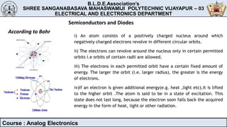
According to Bohr
i) An atom consists of a positively charged nucleus around which
negatively charged electrons revolve in different circular orbits.
ii) The electrons can revolve around the nucleus only in certain permitted
orbits i.e orbits of certain radii are allowed.
iii) The electrons in each permitted orbit have a certain fixed amount of
energy. The larger the orbit (i.e. larger radius), the greater is the energy
of electrons.
iv)If an electron is given additional energy(e.g. heat ,light etc),it is lifted
to the higher orbit .The atom is said to be in a state of excitation. This
state does not last long, because the electron soon falls back the acquired
energy in the form of heat, light or other radiation.
2. B.L.D.E.Association’s
SHREE SANGANABASAVA MAHASWAMIJI POLYTECHNIC VIJAYAPUR – 03
MECHANICAL ENGINEERING DEPARTMENT
B.L.D.E.Association’s
SHREE SANGANABASAVA MAHASWAMIJI POLYTECHNIC VIJAYAPUR – 03
ELECTRICAL AND ELECTRONICS ENGINEERING DEPARTMENT
Course : Analog Electronics
Structure of silicon atom
Valence Electrons:
The electrons in the outermost orbit of an atom are known as valence electrons. The valence electrons determines the
physical (metal or non –metal), chemical (gas or solid) and electrical properties of a material.
The valence electrons of different materials possess different energies. The greater the energy of a valence electrons, the
lesser it is bound to the nucleus.
Free Electrons:
The valence electrons which are very loosely attached to the nucleus are known as “free electrons”.
Thus free electrons moves under various fields and conduct electricity. More the number of free electrons better is the
conductivity.
3. B.L.D.E.Association’s
SHREE SANGANABASAVA MAHASWAMIJI POLYTECHNIC VIJAYAPUR – 03
MECHANICAL ENGINEERING DEPARTMENT
B.L.D.E.Association’s
SHREE SANGANABASAVA MAHASWAMIJI POLYTECHNIC VIJAYAPUR – 03
DEPARTMENT OF MECHANICAL ENGINEERING
Course : Analog Electronics
B.L.D.E.Association’s
SHREE SANGANABASAVA MAHASWAMIJI POLYTECHNIC VIJAYAPUR – 03
ELECTRICAL AND ELECTRONICS ENGINEERING DEPARTMENT
Energy levels:
First figure shows energy levels diagrams .The first orbit
represents the first energy level; the second orbit indicates
the second energy level and so on. The larger the orbit of an
electron, the greater is its energy and higher is the energy
level.
Second figure shows the energy levels of a single isolated
atom. Each orbit of an atom has a single energy. Therefore,
an electron can have only single energy corresponding to
the orbit in which its exist.
An electron possesses two types of energies i.e. kinetic energy due to its motion and potentials energy due to the
charge on the nucleus. The total energy of electrons are the sum of these two energies. The energy of an electron
increases as its distance from the nucleus increases. Thus it is clear that electrons in the last orbit possess very high
energy as compared to electron in the inner orbits.
4. B.L.D.E.Association’s
SHREE SANGANABASAVA MAHASWAMIJI POLYTECHNIC VIJAYAPUR – 03
MECHANICAL ENGINEERING DEPARTMENT
Course : Analog Electronics
B.L.D.E.Association’s
SHREE SANGANABASAVA MAHASWAMIJI POLYTECHNIC VIJAYAPUR – 03
ELECTRICAL AND ELECTRONICS ENGINEERING DEPARTMENT
Energy band
“The range of energies possessed by an electron in a solid is known as energy band”.
All valence electrons cannot become free. Thus there is energy band associated with
valence electrons called valence band.
The energy levels of free electrons also merge into each other to form an energy
band called conduction band.
when the atom is in solid, the electrons in any orbit can have a range of energies.
An energy band which separates the conduction band and the valence band
on energy band level diagram is called forbidden band or forbidden
energy gap denoted as EG.
5. B.L.D.E.Association’s
SHREE SANGANABASAVA MAHASWAMIJI POLYTECHNIC VIJAYAPUR – 03
MECHANICAL ENGINEERING DEPARTMENT
Course : Analog Electronics
B.L.D.E.Association’s
SHREE SANGANABASAVA MAHASWAMIJI POLYTECHNIC VIJAYAPUR – 03
ELECTRICAL AND ELECTRONICS ENGINEERING DEPARTMENT
Based on energy gap Eg, the materials are classified as conductors, insulators
and semiconductors.
Conductors
In terms of energy band ,the valence
and conduction bands are overlapped.
Insulators
In terms of energy band, the valence
band is full while the conduction
band is empty.
Semiconductors
In terms of energy band, the
valence band is almost filled and
conduction band is almost empty.
6. B.L.D.E.Association’s
SHREE SANGANABASAVA MAHASWAMIJI POLYTECHNIC VIJAYAPUR – 03
MECHANICAL ENGINEERING DEPARTMENT
Course : Analog Electronics
B.L.D.E.Association’s
SHREE SANGANABASAVA MAHASWAMIJI POLYTECHNIC VIJAYAPUR – 03
ELECTRICAL AND ELECTRONICS ENGINEERING DEPARTMENT
Properties of Semiconductors:
i) The resistivity of a semiconductor is less than an insulator but more than a conductor.
ii) Semiconductor have negative temperature coefficient of resistance i.e the resistance of a
semiconductor decreases with the increase in temperature and vice-versa.
Ex:Gremanium is actually an insulator at low temperature.
iii) When a suitable metallic impurity (E.g arsenic,gallium etc)is added to a semiconductor to a
semiconductor, its current conducting properties change appreciably.
iv) Semiconducting exhibit a rise in conductivity with increase in temperature and falls off at low
temperature.
7. B.L.D.E.Association’s
SHREE SANGANABASAVA MAHASWAMIJI POLYTECHNIC VIJAYAPUR – 03
MECHANICAL ENGINEERING DEPARTMENT
Course : Analog Electronics
B.L.D.E.Association’s
SHREE SANGANABASAVA MAHASWAMIJI POLYTECHNIC VIJAYAPUR – 03
ELECTRICAL AND ELECTRONICS ENGINEERING DEPARTMENT
Intrinsic Semiconductor
A semiconductor in an extremely pure form is known as an intrinsic semiconductor.
The conductivity of such intrinsic semiconductor is very poor and practically cannot be
used for manufacturing of the semiconductor devices.
Extrinsic Semiconductor
To increase the conducting properties of intrinsic semiconductor, it must be altered
.This is achieved by adding a small amount of suitable impurity to a semiconductor. Such
impure semiconductor is called an extrinsic semiconductor.
Doping: The process of adding impurities to an intrinsic semiconductor is known as
doping .The impurity added is called dopant.
8. B.L.D.E.Association’s
SHREE SANGANABASAVA MAHASWAMIJI POLYTECHNIC VIJAYAPUR – 03
MECHANICAL ENGINEERING DEPARTMENT
Course : Analog Electronics
B.L.D.E.Association’s
SHREE SANGANABASAVA MAHASWAMIJI POLYTECHNIC VIJAYAPUR – 03
ELECTRICAL AND ELECTRONICS ENGINEERING DEPARTMENT
p-type and n-type extrinsic semiconductor
There are two types of impurities used to obtain two different types of extrinsic semiconductors called p-
type and n-type.
The impurity having five valence electrons is called pentavalent impurity. When this is added, its each atom
donates one free electron and such doping is called donor doping. This creates n-type extrinsic
semiconductor.E.x:Arsenic ,bismuth,phosphoraous etc.
9. B.L.D.E.Association’s
SHREE SANGANABASAVA MAHASWAMIJI POLYTECHNIC VIJAYAPUR – 03
MECHANICAL ENGINEERING DEPARTMENT
Course : Analog Electronics
B.L.D.E.Association’s
SHREE SANGANABASAVA MAHASWAMIJI POLYTECHNIC VIJAYAPUR – 03
ELECTRICAL AND ELECTRONICS ENGINEERING DEPARTMENT
The impurity which has three valence electrons is called trivalent impurity .When this is
added, its each atom creates one hole which is ready to accept an electron .Hence this is
called acceptor an electron .Hence this is called acceptor doping. This creates p type
extrinsic semiconductor.
E.x: Gallium, Indium and Boron
10. B.L.D.E.Association’s
SHREE SANGANABASAVA MAHASWAMIJI POLYTECHNIC VIJAYAPUR – 03
MECHANICAL ENGINEERING DEPARTMENT
Course : Analog Electronics
B.L.D.E.Association’s
SHREE SANGANABASAVA MAHASWAMIJI POLYTECHNIC VIJAYAPUR – 03
ELECTRICAL AND ELECTRONICS ENGINEERING DEPARTMENT
Majority Charge Carriers and Minority Charge Carriers:
In n-type materials, the free electrons are large in number than Holes. Hence current is mainly
due to the free electrons. Hence free electrons are majority carriers while Holes are minority
carries in n-type materials.
In p-type material, the holes are large in number then free electrons .Hence current is mainly
due to holes while free electrons are minority carriers in p-type material.
11. B.L.D.E.Association’s
SHREE SANGANABASAVA MAHASWAMIJI POLYTECHNIC VIJAYAPUR – 03
MECHANICAL ENGINEERING DEPARTMENT
Course : Analog Electronics
B.L.D.E.Association’s
SHREE SANGANABASAVA MAHASWAMIJI POLYTECHNIC VIJAYAPUR – 03
ELECTRICAL AND ELECTRONICS ENGINEERING DEPARTMENT
Diffusion:
In given materials, if doping is not uniform then at one side there are large number of charge carriers (either free
electrons or holes) while there are less number of charge carriers on other side .As charge carriers are of similar type,
they start repelling in high concentration area .Thus charge carriers starts moving from high concentration area
towards low concentration area till uniform concentration is achieved all over the material .This process is called
“diffusion”.
Diffusion: Diffusion is a process in which charges move from a region of higher concentration to lower
concentration.
12. B.L.D.E.Association’s
SHREE SANGANABASAVA MAHASWAMIJI POLYTECHNIC VIJAYAPUR – 03
MECHANICAL ENGINEERING DEPARTMENT
Course : Analog Electronics
B.L.D.E.Association’s
SHREE SANGANABASAVA MAHASWAMIJI POLYTECHNIC VIJAYAPUR – 03
ELECTRICAL AND ELECTRONICS ENGINEERING DEPARTMENT
Diode (p-n junction)
When a sample of silicon is doped with both donor and acceptor semiconductor impurities so as to form a region of p-
type and second of n-type material in the same crystal lattice as shown in figure, the boundary where the regions meet is
called a p-n junction i.e when a p-type semiconductor, is suitably joined to an n-type semiconductor. The contact surface
is called p-n junction.
When the two pieces are joined together, they form pnjunction.The
resulting semiconductor devices called p-n junction diode. A diode is so
called because it has two terminal .One is anode, which is the positive
terminal and cathode which is the negative terminal. In case of a p-n
junction diode, the anode is the p-type and cathode is the n-type.
13. B.L.D.E.Association’s
SHREE SANGANABASAVA MAHASWAMIJI POLYTECHNIC VIJAYAPUR – 03
MECHANICAL ENGINEERING DEPARTMENT
Course : Analog Electronics
B.L.D.E.Association’s
SHREE SANGANABASAVA MAHASWAMIJI POLYTECHNIC VIJAYAPUR – 03
ELECTRICAL AND ELECTRONICS ENGINEERING DEPARTMENT
Definition: It is a two layer, two terminal, pn semiconductor device. A p-n junction diode is an
unidirectional device. It can conduct current only in one direction of the conventional current which can
flow when an external voltage is applied.
14. B.L.D.E.Association’s
SHREE SANGANABASAVA MAHASWAMIJI POLYTECHNIC VIJAYAPUR – 03
MECHANICAL ENGINEERING DEPARTMENT
Course : Analog Electronics
B.L.D.E.Association’s
SHREE SANGANABASAVA MAHASWAMIJI POLYTECHNIC VIJAYAPUR – 03
ELECTRICAL AND ELECTRONICS ENGINEERING DEPARTMENT
15. B.L.D.E.Association’s
SHREE SANGANABASAVA MAHASWAMIJI POLYTECHNIC VIJAYAPUR – 03
MECHANICAL ENGINEERING DEPARTMENT
Course : Analog Electronics
B.L.D.E.Association’s
SHREE SANGANABASAVA MAHASWAMIJI POLYTECHNIC VIJAYAPUR – 03
ELECTRICAL AND ELECTRONICS ENGINEERING DEPARTMENT
Formation of depletion region in an unbiased p-n junction
When p-n junction is formed, some of the conduction electrons from n-
type material diffuse into p-type and recombine with holes of acceptor
atoms. This acceptor atom becomes negative immobile ions and
accumulates just near the junction in p-type.
Simultaneously, holes from p-type material diffuse over to the n-
type material and recombine with electrons in donor atoms. This donor
atom becomes positive immobile ions and accumulates near the
junction in n-region.
When a sufficient number of donor and acceptor ions are
uncovered, further diffusion is prevented. Hence this diffusion process
establishes a wall of negative immobile charge on p-side and positive
immobile charge on n side. The region is depleted with immobile charge
carriers, hence it is called depletion region ,depletion layer or space
charge region.
16. B.L.D.E.Association’s
SHREE SANGANABASAVA MAHASWAMIJI POLYTECHNIC VIJAYAPUR – 03
MECHANICAL ENGINEERING DEPARTMENT
Course : Analog Electronics
B.L.D.E.Association’s
SHREE SANGANABASAVA MAHASWAMIJI POLYTECHNIC VIJAYAPUR – 03
ELECTRICAL AND ELECTRONICS ENGINEERING DEPARTMENT
Biasing: Applying external voltage to p-n junction diode is called biasing.
Forward biasing: When an external d.c voltage is connected in such a way that p region is connected to
positive and n region to negative of the d.c voltage then the biasing is called forward biasing.
Or
When external voltage applied to the junction is in such a direction that it cancels the potential barrier,
thus permitting current flow it is called forward biasing.
Figure shows p-n junction under forward biased condition
.When the voltage is increased, electrons and holes move
towards the junction . So that the depletion region
decreases and becomes zero when the applied voltage is
equal to V.Since depletion width is zero and the diode offers
zero resistance .Thus a forward biased p-n junction behaves
like a closed switch.
17. B.L.D.E.Association’s
SHREE SANGANABASAVA MAHASWAMIJI POLYTECHNIC VIJAYAPUR – 03
MECHANICAL ENGINEERING DEPARTMENT
Course : Analog Electronics
B.L.D.E.Association’s
SHREE SANGANABASAVA MAHASWAMIJI POLYTECHNIC VIJAYAPUR – 03
ELECTRICAL AND ELECTRONICS ENGINEERING DEPARTMENT
Reverse biased condition
When an external dc voltage is connected in such a way that p-region is connected to negative and n-region
to positive terminal of the d.c voltage then the biasing is called reverse biasing.
Or
When the external voltage applied to the junction is in direction that potential barrier is increased, it is
called reverse biasing.
Figure shows a p-n junction under reverse biased condition
.When reverse voltage is applied, majority carriers move
away from the junction. So that the depletion width start
increasing. The diode is known offers very high resistance
behaves like an open switch.
Due to the presence of a small number of minority
carriers a very small reverse saturation current flows through
the diode (1-2µA).This is also called the leakage current.
18. B.L.D.E.Association’s
SHREE SANGANABASAVA MAHASWAMIJI POLYTECHNIC VIJAYAPUR – 03
MECHANICAL ENGINEERING DEPARTMENT
Course : Analog Electronics
V_ I Characteristics of p-n junction
a) Zero external voltage: With zero external voltage the potential circuit behaves like a open circuit and not allowed
the current to flow as indicated by ‘O’ in figure (a).
B.L.D.E.Association’s
SHREE SANGANABASAVA MAHASWAMIJI POLYTECHNIC VIJAYAPUR – 03
ELECTRICAL AND ELECTRONICS ENGINEERING DEPARTMENT
19. B.L.D.E.Association’s
SHREE SANGANABASAVA MAHASWAMIJI POLYTECHNIC VIJAYAPUR – 03
MECHANICAL ENGINEERING DEPARTMENT
Course : Analog Electronics
b) Forward bias: With forward bias to the p-n junction, the potential barrier is start
reducing .At some forward voltage (0.7v for Si and 0.3V for Ge) the potential barrier is
altogether eliminated and current starts flowing in the circuit .From this, the current
increases with the increase in forward voltage .Thus rising curve OB is obtained with
forward bias as shown in figure. In region OA, the current increases very slowly and the
curve is non-linear. In region AB, the current increases very sharply and curve is almost
linear and diode behaves an ordinary conductor.
c) Reverse bias: With reverse bias to pn junction potential barrier start increasing at
the junction .Therefore junction resistance becomes very high and practically no
current flows through the circuit .However in the reverse characteristics a very small
(in µA) flows in the circuit with reverse bias .This is called reverse saturation current ‘Is’
and it is due to minority carriers.
B.L.D.E.Association’s
SHREE SANGANABASAVA MAHASWAMIJI POLYTECHNIC VIJAYAPUR – 03
ELECTRICAL AND ELECTRONICS ENGINEERING DEPARTMENT
20. B.L.D.E.Association’s
SHREE SANGANABASAVA MAHASWAMIJI POLYTECHNIC VIJAYAPUR – 03
MECHANICAL ENGINEERING DEPARTMENT
Course : Analog Electronics
P-N Junction Diode Applications
• It is used in clipping circuits as wave shaping circuits in computers, radios, radars etc.
• It is used as switches in digital logic designs.
• It is used in detector and demodulator circuits.
• It is used in clamping circuits in TV receivers as well as voltage multipliers.
• It is used as rectifiers in DC power supply manufacturing.
B.L.D.E.Association’s
SHREE SANGANABASAVA MAHASWAMIJI POLYTECHNIC VIJAYAPUR – 03
ELECTRICAL AND ELECTRONICS ENGINEERING DEPARTMENT