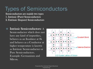
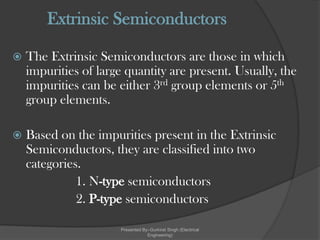
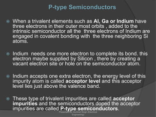
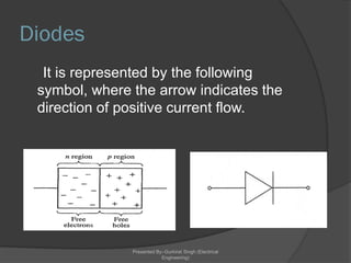
SEMICONDUCTOR PHYSICS
PRESENTED BY:- GURKIRAT SINGH
Overview
 Atomic Bonding
 Energy Bands
 Resistivity
 Electronic Materials
 Semiconductors
 Types of Semiconductors
 P-type and N-type semiconductors
 Diodes
Presented By:-Gurkirat Singh (Electrical
Engineering)
Atomic Bonds
 Atomic bonding is chemical bonding. Chemical
bonding is the physical process that is responsible
for the interactions between atoms and molecules.
Bonds vary widely; there are covalent, ionic,
hydrogen, metallic, as well as many other types of
bonds.
Presented By:-Gurkirat Singh (Electrical
Engineering)
Types of Atomic Bonds
 Metallic Bond
Metallic bonds are a metal, and share outer bonds
with atoms in a solid. Each atom gives off a positive
charge by shedding (give off) its outer electrons, and the
negatively charges electrons hold the metal atoms
together.
Presented By:-Gurkirat Singh (Electrical
Engineering)
 Ionic Bond
Atoms are filled with an outer shell of electrons.
Electron shells are filled by transferring electrons
from one atom to the next. Donor atoms will take on
a positive charge, and the acceptors will have a
negative charge. They will attract each other by
being positive and negative, and bonding will then
occur.
 Covalent Bonds
Atoms like to share their electrons and this
causes their outer shell to be complete. A covalent
bond is produced by the sharing of atoms and
electrons. This produces a strong covalent bond.
Presented By:-Gurkirat Singh (Electrical
Engineering)
Presented By:-Gurkirat Singh (Electrical
Engineering)
Energy bands
 The intermixing of atoms in solids,
instead of single energy levels, there will
be bands of energy levels formed.
These set of energy levels, which are
closely packed are called as Energy
bands.
Presented By:-Gurkirat Singh (Electrical
Engineering)
Classification of Energy Bands
 Valance Band : The electrons
that are present in the
outermost shell, containing a
series of energy levels, form
an energy band which is
called as Valence Band.
The valence band is
the band having the highest
occupied energy.
 Conduction Band :
These free electrons are
the ones which conduct
the current in a
conductor and hence
called as Conduction
Electrons. The band
which contains
conduction electrons is
called as Conduction
Band. The conduction
band is the band having
the lowest occupied
energy.
Presented By:-Gurkirat Singh (Electrical
Engineering)
 Forbidden gap : The gap between valence band and
conduction band is called as forbidden energy gap. As the
name implies, this band is the forbidden one without energy.
Hence no electron stays in this band. The valence electrons,
while going to the conduction band, pass through this.
 The following figure shows the structure of energy bands in
solids.
Presented By:-Gurkirat Singh (Electrical
Engineering)
Resistivity
 The electrical Resistance of an electrical or
electronic component or device is generally
defined as being the ratio of the voltage difference
across it to the current flowing through it,
basic Ohm´s Law principals. The quantity that is
used to indicate this specific resistance is
called Resistivity and is given the Greek symbol
of ρ, (Rho). Resistivity is measured in Ohm-
metres, (Ω.m ). Resistivity is the inverse to
conductivity.
Presented By:-Gurkirat Singh (Electrical
Engineering)
Presented By:-Gurkirat Singh (Electrical
Engineering)
Electronic Materials
 The goal of electronic materials is to
generate and control the flow of an
electrical current.
 Electronic materials include:
1. Conductors: have low resistance which
allows electrical current flow
2. Insulators: have high resistance which
suppresses electrical current flow
3. Semiconductors: can allow or suppress
electrical current flow
Presented By:-Gurkirat Singh (Electrical
Engineering)
Semiconductors
 Semiconductors are
materials that essentially
can be conditioned to act
as good conductors, or
good insulators, or any
thing in between.
 Common elements such
as carbon, silicon, and
germanium are
semiconductors.
 Silicon is the best and
most widely used
semiconductor.
 Low resistivity =>
“conductor”
 High resistivity =>
“insulator”
 Intermediate
resistivity =>
“semiconductor”
 conductivity lies
between that of
conductors and
insulators
 generally crystalline
in structure for IC
devices
Presented By:-Gurkirat Singh (Electrical
Engineering)
Semiconductor Materials
Presented By:-Gurkirat Singh (Electrical
Engineering)
Semiconductor Valence Orbit
 The main
characteristic of a
semiconductor
element is that it has
four electrons in its
outer or valence
orbit.
Presented By:-Gurkirat Singh (Electrical
Engineering)
Crystal Lattice Structure
2D Crystal Lattice Structure
 The unique capability of
semiconductor atoms is
their ability to link
together to form a
physical structure called
a crystal lattice.
 The atoms link together
with one another sharing
their outer electrons.
 These links are called
covalent bonds.
Presented By:-Gurkirat Singh (Electrical
Engineering)
3D Crystal Lattice Structure
Presented By:-Gurkirat Singh (Electrical
Engineering)
Types of Semiconductors
Semiconductors are mainly two types
1. Intrinsic (Pure) Semiconductors
2. Extrinsic (Impure) Semiconductors
 Intrinsic Semiconductors: A
Semiconductor which does not
have any kind of impurities,
behaves as an Insulator at 0k
and behaves as a Conductor at
higher temperature is known
as Intrinsic Semiconductor or
Pure Semiconductors.
Example: Germanium and
Silicon.
Presented By:-Gurkirat Singh (Electrical
Engineering)
Extrinsic Semiconductors
 The Extrinsic Semiconductors are those in which
impurities of large quantity are present. Usually, the
impurities can be either 3rd group elements or 5th
group elements.
 Based on the impurities present in the Extrinsic
Semiconductors, they are classified into two
categories.
1. N-type semiconductors
2. P-type semiconductors
Presented By:-Gurkirat Singh (Electrical
Engineering)
 When any pentavalent element such as Phosphorous,
Arsenic or Antimony is added to the intrinsic
Semiconductor , four electrons are involved in covalent
bonding with four neighboring pure Semiconductor atoms.
 The fifth electron is weakly bound to the parent atom. And
even for lesser thermal energy it is released Leaving the
parent atom positively ionized. The Intrinsic
Semiconductors doped with pentavalent impurities are
called N-type Semiconductors.
 The energy level of fifth electron is called donor level. The
donor level is close to the bottom of the conduction band
most of the donor level electrons are excited in to the
conduction band at room temperature and become the
Majority charge carriers.
 Hence in N-type Semiconductors electrons are Majority
carriers and holes are Minority carriers.
N - type Semiconductors
Presented By:-Gurkirat Singh (Electrical
Engineering)
P-type Semiconductors
 When a trivalent elements such as Al, Ga or Indium have
three electrons in their outer most orbits , added to the
intrinsic semiconductor all the three electrons of Indium are
engaged in covalent bonding with the three neighboring Si
atoms.
 Indium needs one more electron to complete its bond. this
electron maybe supplied by Silicon , there by creating a
vacant electron site or hole on the semiconductor atom.
 Indium accepts one extra electron, the energy level of this
impurity atom is called acceptor level and this acceptor
level lies just above the valence band.
 These type of trivalent impurities are called acceptor
impurities and the semiconductors doped the acceptor
impurities are called P-type semiconductors.Presented By:-Gurkirat Singh (Electrical
Engineering)
2D Crystal Lattice Structure of Silicon Doped
with (i) Boron (ii) Phosphorus
Presented By:-Gurkirat Singh (Electrical
Engineering)
Diodes
Electronic devices created by bringing
together a p-type and n-type region
within the same semiconductor lattice.
Used for rectifiers, LED etc
Presented By:-Gurkirat Singh (Electrical
Engineering)
Diodes
It is represented by the following
symbol, where the arrow indicates the
direction of positive current flow.
Presented By:-Gurkirat Singh (Electrical
Engineering)
Forward Bias and Reverse Bias
 Forward Bias : Connect positive of the
Diode to positive of supply…negative of
Diode to negative of supply
 Reverse Bias: Connect positive of the
Diode to negative of supply…negative of
diode to positive of supply.
Presented By:-Gurkirat Singh (Electrical
Engineering)
Characteristics of Diode
 Diode always conducts in one direction.
 Diodes always conduct current when
“Forward Biased” ( Zero resistance)
 Diodes do not conduct when Reverse
Biased
(Infinite resistance)
Presented By:-Gurkirat Singh (Electrical
Engineering)
I-V characteristics of Ideal diode
Presented By:-Gurkirat Singh (Electrical
Engineering)
I-V Characteristics of Practical Diode
Presented By:-Gurkirat Singh (Electrical
Engineering)
Rectification
 Converting ac to dc is accomplished by
the process of rectification.
 Two processes are used:
 Half-wave rectification;
 Full-wave rectification.
Presented By:-Gurkirat Singh (Electrical
Engineering)
Half-wave Rectification
 Simplest process
used to convert ac to
dc.
 A diode is used to
clip the input signal
excursions of one
polarity to zero.
Presented By:-Gurkirat Singh (Electrical
Engineering)
Terminology
donor: impurity atom that increases n
acceptor: impurity atom that increases p
N-type material: contains more electrons than holes
P-type material: contains more holes than electrons
majority carrier: the most abundant carrier
minority carrier: the least abundant carrier
intrinsic semiconductor: n = p = ni
extrinsic semiconductor: doped semiconductor
Presented By:-Gurkirat Singh (Electrical
Engineering)
Summary
 The band gap energy is the energy required to free
an electron from a covalent bond.
 Eg for Si at 300K = 1.12eV
 In a pure Si crystal, conduction electrons and holes
are formed in pairs.
 Holes can be considered as positively charged mobile
particles which exist inside a semiconductor.
 Both holes and electrons can conduct current.
 Substitutional dopants in Si:
 Group-V elements (donors) contribute conduction
electrons
 Group-III elements (acceptors) contribute holes
 Very low ionization energies (<50 meV)
Presented By:-Gurkirat Singh (Electrical
Engineering)
Presented By:-Gurkirat Singh (Electrical
Engineering)

Semiconductor physics electronic devices

  • 1.
  • 2.
    Overview  Atomic Bonding Energy Bands  Resistivity  Electronic Materials  Semiconductors  Types of Semiconductors  P-type and N-type semiconductors  Diodes Presented By:-Gurkirat Singh (Electrical Engineering)
  • 3.
    Atomic Bonds  Atomicbonding is chemical bonding. Chemical bonding is the physical process that is responsible for the interactions between atoms and molecules. Bonds vary widely; there are covalent, ionic, hydrogen, metallic, as well as many other types of bonds. Presented By:-Gurkirat Singh (Electrical Engineering)
  • 4.
    Types of AtomicBonds  Metallic Bond Metallic bonds are a metal, and share outer bonds with atoms in a solid. Each atom gives off a positive charge by shedding (give off) its outer electrons, and the negatively charges electrons hold the metal atoms together. Presented By:-Gurkirat Singh (Electrical Engineering)
  • 5.
     Ionic Bond Atomsare filled with an outer shell of electrons. Electron shells are filled by transferring electrons from one atom to the next. Donor atoms will take on a positive charge, and the acceptors will have a negative charge. They will attract each other by being positive and negative, and bonding will then occur.  Covalent Bonds Atoms like to share their electrons and this causes their outer shell to be complete. A covalent bond is produced by the sharing of atoms and electrons. This produces a strong covalent bond. Presented By:-Gurkirat Singh (Electrical Engineering)
  • 6.
    Presented By:-Gurkirat Singh(Electrical Engineering)
  • 7.
    Energy bands  Theintermixing of atoms in solids, instead of single energy levels, there will be bands of energy levels formed. These set of energy levels, which are closely packed are called as Energy bands. Presented By:-Gurkirat Singh (Electrical Engineering)
  • 8.
    Classification of EnergyBands  Valance Band : The electrons that are present in the outermost shell, containing a series of energy levels, form an energy band which is called as Valence Band. The valence band is the band having the highest occupied energy.  Conduction Band : These free electrons are the ones which conduct the current in a conductor and hence called as Conduction Electrons. The band which contains conduction electrons is called as Conduction Band. The conduction band is the band having the lowest occupied energy. Presented By:-Gurkirat Singh (Electrical Engineering)
  • 9.
     Forbidden gap: The gap between valence band and conduction band is called as forbidden energy gap. As the name implies, this band is the forbidden one without energy. Hence no electron stays in this band. The valence electrons, while going to the conduction band, pass through this.  The following figure shows the structure of energy bands in solids. Presented By:-Gurkirat Singh (Electrical Engineering)
  • 10.
    Resistivity  The electricalResistance of an electrical or electronic component or device is generally defined as being the ratio of the voltage difference across it to the current flowing through it, basic Ohm´s Law principals. The quantity that is used to indicate this specific resistance is called Resistivity and is given the Greek symbol of ρ, (Rho). Resistivity is measured in Ohm- metres, (Ω.m ). Resistivity is the inverse to conductivity. Presented By:-Gurkirat Singh (Electrical Engineering)
  • 11.
    Presented By:-Gurkirat Singh(Electrical Engineering)
  • 12.
    Electronic Materials  Thegoal of electronic materials is to generate and control the flow of an electrical current.  Electronic materials include: 1. Conductors: have low resistance which allows electrical current flow 2. Insulators: have high resistance which suppresses electrical current flow 3. Semiconductors: can allow or suppress electrical current flow Presented By:-Gurkirat Singh (Electrical Engineering)
  • 13.
    Semiconductors  Semiconductors are materialsthat essentially can be conditioned to act as good conductors, or good insulators, or any thing in between.  Common elements such as carbon, silicon, and germanium are semiconductors.  Silicon is the best and most widely used semiconductor.  Low resistivity => “conductor”  High resistivity => “insulator”  Intermediate resistivity => “semiconductor”  conductivity lies between that of conductors and insulators  generally crystalline in structure for IC devices Presented By:-Gurkirat Singh (Electrical Engineering)
  • 14.
    Semiconductor Materials Presented By:-GurkiratSingh (Electrical Engineering)
  • 15.
    Semiconductor Valence Orbit The main characteristic of a semiconductor element is that it has four electrons in its outer or valence orbit. Presented By:-Gurkirat Singh (Electrical Engineering)
  • 16.
    Crystal Lattice Structure 2DCrystal Lattice Structure  The unique capability of semiconductor atoms is their ability to link together to form a physical structure called a crystal lattice.  The atoms link together with one another sharing their outer electrons.  These links are called covalent bonds. Presented By:-Gurkirat Singh (Electrical Engineering)
  • 17.
    3D Crystal LatticeStructure Presented By:-Gurkirat Singh (Electrical Engineering)
  • 18.
    Types of Semiconductors Semiconductorsare mainly two types 1. Intrinsic (Pure) Semiconductors 2. Extrinsic (Impure) Semiconductors  Intrinsic Semiconductors: A Semiconductor which does not have any kind of impurities, behaves as an Insulator at 0k and behaves as a Conductor at higher temperature is known as Intrinsic Semiconductor or Pure Semiconductors. Example: Germanium and Silicon. Presented By:-Gurkirat Singh (Electrical Engineering)
  • 19.
    Extrinsic Semiconductors  TheExtrinsic Semiconductors are those in which impurities of large quantity are present. Usually, the impurities can be either 3rd group elements or 5th group elements.  Based on the impurities present in the Extrinsic Semiconductors, they are classified into two categories. 1. N-type semiconductors 2. P-type semiconductors Presented By:-Gurkirat Singh (Electrical Engineering)
  • 20.
     When anypentavalent element such as Phosphorous, Arsenic or Antimony is added to the intrinsic Semiconductor , four electrons are involved in covalent bonding with four neighboring pure Semiconductor atoms.  The fifth electron is weakly bound to the parent atom. And even for lesser thermal energy it is released Leaving the parent atom positively ionized. The Intrinsic Semiconductors doped with pentavalent impurities are called N-type Semiconductors.  The energy level of fifth electron is called donor level. The donor level is close to the bottom of the conduction band most of the donor level electrons are excited in to the conduction band at room temperature and become the Majority charge carriers.  Hence in N-type Semiconductors electrons are Majority carriers and holes are Minority carriers. N - type Semiconductors Presented By:-Gurkirat Singh (Electrical Engineering)
  • 21.
    P-type Semiconductors  Whena trivalent elements such as Al, Ga or Indium have three electrons in their outer most orbits , added to the intrinsic semiconductor all the three electrons of Indium are engaged in covalent bonding with the three neighboring Si atoms.  Indium needs one more electron to complete its bond. this electron maybe supplied by Silicon , there by creating a vacant electron site or hole on the semiconductor atom.  Indium accepts one extra electron, the energy level of this impurity atom is called acceptor level and this acceptor level lies just above the valence band.  These type of trivalent impurities are called acceptor impurities and the semiconductors doped the acceptor impurities are called P-type semiconductors.Presented By:-Gurkirat Singh (Electrical Engineering)
  • 22.
    2D Crystal LatticeStructure of Silicon Doped with (i) Boron (ii) Phosphorus Presented By:-Gurkirat Singh (Electrical Engineering)
  • 23.
    Diodes Electronic devices createdby bringing together a p-type and n-type region within the same semiconductor lattice. Used for rectifiers, LED etc Presented By:-Gurkirat Singh (Electrical Engineering)
  • 24.
    Diodes It is representedby the following symbol, where the arrow indicates the direction of positive current flow. Presented By:-Gurkirat Singh (Electrical Engineering)
  • 25.
    Forward Bias andReverse Bias  Forward Bias : Connect positive of the Diode to positive of supply…negative of Diode to negative of supply  Reverse Bias: Connect positive of the Diode to negative of supply…negative of diode to positive of supply. Presented By:-Gurkirat Singh (Electrical Engineering)
  • 26.
    Characteristics of Diode Diode always conducts in one direction.  Diodes always conduct current when “Forward Biased” ( Zero resistance)  Diodes do not conduct when Reverse Biased (Infinite resistance) Presented By:-Gurkirat Singh (Electrical Engineering)
  • 27.
    I-V characteristics ofIdeal diode Presented By:-Gurkirat Singh (Electrical Engineering)
  • 28.
    I-V Characteristics ofPractical Diode Presented By:-Gurkirat Singh (Electrical Engineering)
  • 29.
    Rectification  Converting acto dc is accomplished by the process of rectification.  Two processes are used:  Half-wave rectification;  Full-wave rectification. Presented By:-Gurkirat Singh (Electrical Engineering)
  • 30.
    Half-wave Rectification  Simplestprocess used to convert ac to dc.  A diode is used to clip the input signal excursions of one polarity to zero. Presented By:-Gurkirat Singh (Electrical Engineering)
  • 31.
    Terminology donor: impurity atomthat increases n acceptor: impurity atom that increases p N-type material: contains more electrons than holes P-type material: contains more holes than electrons majority carrier: the most abundant carrier minority carrier: the least abundant carrier intrinsic semiconductor: n = p = ni extrinsic semiconductor: doped semiconductor Presented By:-Gurkirat Singh (Electrical Engineering)
  • 32.
    Summary  The bandgap energy is the energy required to free an electron from a covalent bond.  Eg for Si at 300K = 1.12eV  In a pure Si crystal, conduction electrons and holes are formed in pairs.  Holes can be considered as positively charged mobile particles which exist inside a semiconductor.  Both holes and electrons can conduct current.  Substitutional dopants in Si:  Group-V elements (donors) contribute conduction electrons  Group-III elements (acceptors) contribute holes  Very low ionization energies (<50 meV) Presented By:-Gurkirat Singh (Electrical Engineering)
  • 33.
    Presented By:-Gurkirat Singh(Electrical Engineering)