Download as PDF, PPTX

![Chun-Feng Chen NCTU_IEE - PCS Lab
Introduction
• Algorithmic Multi-ported Memory (AMM)
• Multi-ported memories are important functional modules in modern digital systems
• E.g. shared cache in multi-core processors, routing tables of switches, etc.
• AMM composes simple SRAMs and logic to support multiple reads and writes
• Potential to attain better performance than circuit-based approaches (CMM)
• Most of the previous works on FPGA
• Laforest, Charles Eric, et al. "Efficient Multi-ported Memories for FPGAs" [ACM 2010]
• Charles Eric Laforest, et al. "Multi-ported Memories for FPGAs via XOR" [ACM 2012]
• Charles Eric Laforest, et al. "Composing Multi-Ported Memories on FPGAs" [ACM 2014]
• Jiun-Liang Lin, et al. "BRAM Efficient Multi-ported Memory on FPGAs" [VLSI-DAT 2015]
• Jiun-Liang Lin, et al. "Efficient Designs of Multi-ported Memory on FPGAs" [TVLSI 2016]
• Kun-Hua Huang, et al. "An Efficient Hierarchical Banking Structure for Algorithmic Multi-
ported Memory on FPGAs" [TVLSI 2017]
• Sundar Iyer, et al. "Algorithmic Memory Brings an Order of Magnitude Performance Increase
to Next Generation SoC Memories" [DesignCon 2012]
4](https://image.slidesharecdn.com/amm-oral0308-finalv2-180424155056/85/Algorithmic-Multi-ported-Memory-MEM-Comprehensive-Techniques-Guideline-4-320.jpg)

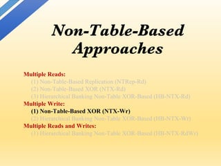
![• Non-table-based schemes
• Duplicate memory module
• E.g. NTRep-Rd [ACM 2010]
• Table-based schemes
• Adopt lookup tables to track the
stored up-to-date data address
• E.g. TBLVT [ACM 2010]
Chun-Feng Chen NCTU_IEE - PCS Lab
Algorithmic Multi-ported Memory
(AMM) Techniques Categorize
8](https://image.slidesharecdn.com/amm-oral0308-finalv2-180424155056/85/Algorithmic-Multi-ported-Memory-MEM-Comprehensive-Techniques-Guideline-8-320.jpg)
![• Non-table-based approaches
• Use multiple banks to support multiple accesses
• Store parity data to support multiple reads and enable multiple
writes [VLSI-DAT’15, TVLSI’16, TVLSI’17]
• HB-NTX-RdWr can scale the number of ports with a systematic flow
[TVLSI’17]
• Table-based approaches
• Use multiple memory modules to support multiple accesses
• Use lookup tables to avoid module conflict and track the most up-to-
date values [VLSI-DAT’ 15, TVLSI’ 16, TVLSI’ 17]
Chun-Feng Chen NCTU_IEE - PCS Lab
AMM - Previous Proposed Designs
9](https://image.slidesharecdn.com/amm-oral0308-finalv2-180424155056/85/Algorithmic-Multi-ported-Memory-MEM-Comprehensive-Techniques-Guideline-9-320.jpg)
![• A mR1W memory module of
NTRep-Rd technique
• Duplicate memory modules to
support multiple read ports
• Only one write port connects each
memory module
[7] LaForest, Charles Eric, and J. Gregory Steffan. "Efficient Multi-ported Memories for FPGAs." Proceedings of the 18th Annual
ACM/SIGDA International Symposium on Field Programmable Gate Arrays (FPGAs). ACM, 2010.
Chun-Feng Chen NCTU_IEE - PCS Lab
Non-Table-Based Replication Multiple
Reads (NTRep-Rd) - [ACM’10, TRETs’14]
12](https://image.slidesharecdn.com/amm-oral0308-finalv2-180424155056/85/Algorithmic-Multi-ported-Memory-MEM-Comprehensive-Techniques-Guideline-12-320.jpg)
![• A 2R1W memory module of NTX-
Rd technique
• Write request
• W0 stores directly to BANK0 and
read D0 from BANK1
• Update the XOR-BANK
• Read request
• R1 reads directly
• R0 reads the other banks to
recover correct data
• NTX-Rd support two mode
• Case 1: 3R (no write request)
• Case 2: 2R1W (one write request)
[13] Sundar Iyer, Shang-Tse Chuang, and Co-Founder & CTO Memoir Systems. " Algorithmic Memory: An Order of Magnitude
Performance Increase for Next Generation SoCs." DesignCon. (http://www.designcon.com), 2012.
Chun-Feng Chen NCTU_IEE - PCS Lab
Non-Table-Based XOR Multiple Reads
(NTX-Rd) - [DesignCon.’12]
W0’ = (W0 D0)
R0 = (W0 D0) D0
W0’
14](https://image.slidesharecdn.com/amm-oral0308-finalv2-180424155056/85/Algorithmic-Multi-ported-Memory-MEM-Comprehensive-Techniques-Guideline-14-320.jpg)
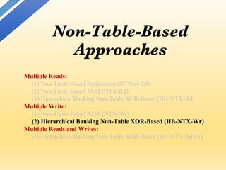
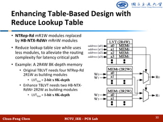
![Hierarchical Banking Non-Table XOR-Based
Multiple Reads (HB-NTX-Rd) - [TVLSI’17]
[12] Lai, Bo-Cheng Charles, and Kun-Hua Huang. "An Efficient Hierarchical Banking Structure for Algorithmic Multiported Memory on
FPGAs." IEEE Transactions on Very Large Scale Integration (VLSI) Systems 25.10 (2017): 2776-2788.
Chun-Feng Chen NCTU_IEE - PCS Lab
• 4 read and 1 write memory
• Scale the B-NTX-Rd to more reads in a
hierarchical structure
• Use the 2R1W/3R as building modules
• Case 1: 5R (no write request)
• Three reads access BANK0
• Other two reads access the other banks
• Case 2: 4R1W (one write request)
• W0 and two reads access BANK0
• Other two reads access the other banks
• W0 stores directly, and reads BANK1 for
updating XOR-BANK
16](https://image.slidesharecdn.com/amm-oral0308-finalv2-180424155056/85/Algorithmic-Multi-ported-Memory-MEM-Comprehensive-Techniques-Guideline-16-320.jpg)
![• A 1R2W memory module of NTX-Wr technique
• Duplicate memory modules and store XOR-encoded values to support multiple
read and writes
[9] LaForest, Charles Eric, et al. "Multi-ported Memories for FPGAs via XOR.” Proceedings of the ACM/SIGDA International Symposium on
Field Programmable Gate Arrays (FPGAs). ACM, 2012.
Chun-Feng Chen NCTU_IEE - PCS Lab
Non-Table-Based XOR Multiple Writes
(NTX-Wr) - [ACM’12, TRETs’14]
W0’ = (W0 D0) D0
W1’ = (W1 D1) D1
W0’ W0’
W1’
W1’
18](https://image.slidesharecdn.com/amm-oral0308-finalv2-180424155056/85/Algorithmic-Multi-ported-Memory-MEM-Comprehensive-Techniques-Guideline-18-320.jpg)
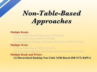
![[12] Lai, Bo-Cheng Charles, and Kun-Hua Huang. "An Efficient Hierarchical Banking Structure for Algorithmic Multiported Memory on
FPGAs." IEEE Transactions on Very Large Scale Integration (VLSI) Systems 25.10 (2017): 2776-2788.
Chun-Feng Chen NCTU_IEE - PCS Lab
Hierarchical Banking Non-Table XOR-Based
Multiple Writes (HB-NTX-Wr) - [TVLSI’17]
(a) Non-Conflict-Write case (b) Conflict-Write case
W0’ = W0 Ref0
W1’ = W1 Ref1
Ref1new = W1 (D0 Ref1cur)
W1’’ = D1 Ref1new
W1’
W0’
W1’’
20](https://image.slidesharecdn.com/amm-oral0308-finalv2-180424155056/85/Algorithmic-Multi-ported-Memory-MEM-Comprehensive-Techniques-Guideline-20-320.jpg)
![• 2 read and 2 write memory
• Integrates HB-NTX-Rd and HB-NTX-Wr to enable multiple reads and writes
• Use HB-NTX-Rd 4R1W/5R as building memory modules
(b) Conflict-Write case(a) Non-Conflict-Write case
Chun-Feng Chen NCTU_IEE - PCS Lab
Hierarchical Banking Non-Table XOR-Based Multiple
Reads and Writes (HB-NTX-RdWr) - [TVLSI’17]
[12] Lai, Bo-Cheng Charles, and Kun-Hua Huang. "An Efficient Hierarchical Banking Structure for Algorithmic Multiported Memory on
FPGAs." IEEE Transactions on Very Large Scale Integration (VLSI) Systems 25.10 (2017): 2776-2788.
22](https://image.slidesharecdn.com/amm-oral0308-finalv2-180424155056/85/Algorithmic-Multi-ported-Memory-MEM-Comprehensive-Techniques-Guideline-22-320.jpg)
![• The top-down flow increases read ports with HB-NTX-Rd, while the left-
right flow increases write ports with HB-NTX-Wr
Chun-Feng Chen NCTU_IEE - PCS Lab
HB-NTX-RdWr Systematic Flow
- [TVLSI’17]
23](https://image.slidesharecdn.com/amm-oral0308-finalv2-180424155056/85/Algorithmic-Multi-ported-Memory-MEM-Comprehensive-Techniques-Guideline-23-320.jpg)

![[7] LaForest, Charles Eric, and J. Gregory Steffan. "Efficient Multi-ported Memories for FPGAs." Proceedings of the 18th Annual
ACM/SIGDA International Symposium on Field Programmable Gate Arrays (FPGAs). ACM, 2010.
Chun-Feng Chen NCTU_IEE - PCS Lab
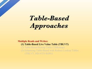
Table-Based Live Value Table (TBLVT)
- [ACM’10, TRETs’14]
• Write request
• Dedicate a write data to a certain
memory module
• Lookup table (LVT) traces the latest
location
• Read request will query the LVT first
and then access the data from correct
memory location
• Design of the LVT size:
• log2(#NumModules) x MemoryDepth
26](https://image.slidesharecdn.com/amm-oral0308-finalv2-180424155056/85/Algorithmic-Multi-ported-Memory-MEM-Comprehensive-Techniques-Guideline-26-320.jpg)
![[11] Lai, Bo-Cheng Charles, and Jiun-Liang Lin. "Efficient Designs of Multi-ported Memory on FPGAs." IEEE Transactions on Very Large
Scale Integration (VLSI) Systems 25.1 (2017): 139-150.
Chun-Feng Chen NCTU_IEE - PCS Lab
Table-Based Remap (TBRemap)
– [VLSI-DAT’15, TVLSI’16]
• Remap functions:
• Apply banking structure designs
• All the reads and writes need to check
remap table to determine which
memory bank to access
• Use a HWC to distribute the multiple
write into writes, and a remap table to
track the latest location
• Design of the Remap size:
• ([log2(#DataBanks + 1)] – 1) x
MemoryDepth
28](https://image.slidesharecdn.com/amm-oral0308-finalv2-180424155056/85/Algorithmic-Multi-ported-Memory-MEM-Comprehensive-Techniques-Guideline-28-320.jpg)


![Chun-Feng Chen NCTU_IEE - PCS Lab
References
•[1] Abdel-Hafeez, Saleh M., and Anas S. Matalkah. "CMOS eight-transistor memory cell for low-dynamic-power high-speed embedded
SRAM." Journal of Circuits, Systems, and Computers 17.05 (2008): 845-863.
•[2] Bhagyalakshmi, I. V., Ravi Teja, and Madhan Mohan. "Design and VLSI Simulation of SRAM Memory Cells for Multi-ported SRAM’s." (2014).
•[3] Rivest, Ronald L., and Lance A. Glasser. A Fast-Multiport Memory Based on Single-Port Memory Cells. No. MIT/LCS/TM-455. MASSACHUSETTS
INST OF TECH CAMBRIDGE LAB FOR COMPUTER SCIENCE, 1991.
•[4] Park, Seon-yeong, et al. "CFLRU: a replacement algorithm for flash memory." Proceedings of the 2006 international conference on Compilers,
architecture and synthesis for embedded systems. ACM, 2006.
•[5] Synopsys Design Compiler User Guide Version X-2005.09. [Online] Available:
http://beethoven.ee.ncku.edu.tw/testlab/course/VLSIdesign_course/course_96/Tool/Design_Compiler%20_User_Guide.pdf
•[6] Synopsys Design Compiler Optimization Reference Manual Version D-2010.03. [Online] Available: http://cleroux.vvv.enseirb-
matmeca.fr/EN219/doc/dcrmo.pdf
•[7] LaForest, Charles Eric, and J. Gregory Steffan. "Efficient Multi-ported Memories for FPGAs." Proceedings of the 18th annual ACM/SIGDA
international symposium on Field programmable gate arrays (FPGA), pp. 41-50, ACM, 2010.
•[8] Charles Eric LaForest, Ming Gang Liu, Emma Rae Rapati, and J. Gregory Steffan. "Multi-ported Memories for FPGAs via XOR," In Proceedings of the
20th annual ACM/SIGDA International Symposium on Field Programmable Gate Arrays (FPGA), pp. 209–218, ACM, 2012.
•[9] Charles Eric Laforest, Zimo Li, Tristan O'rourke, Ming G. Liu, and J. Gregory Steffan. "Composing Multi-Ported Memories on FPGAs," in
Proceedings of the ACM Transactions on Reconfigurable Technology and Systems (TRETS), vol.7, issue 3, article no. 16, 2014.
•[10] Lin, Jiun-Liang, and Bo-Cheng Charles Lai. "BRAM Efficient Multi-ported Memory on FPGA." VLSI Design, Automation and Test (VLSI-DAT), 2015
International Symposium on. IEEE, 2015.
•[11] Lai, Bo-Cheng Charles, and Jiun-Liang Lin. "Efficient Designs of Multiported Memory on FPGA." IEEE Transactions on Very Large Scale Integration
(VLSI) Systems (2016).
65](https://image.slidesharecdn.com/amm-oral0308-finalv2-180424155056/85/Algorithmic-Multi-ported-Memory-MEM-Comprehensive-Techniques-Guideline-65-320.jpg)
![Chun-Feng Chen NCTU_IEE - PCS Lab
References
•[12] Lai, Bo-Cheng Charles, and Kun-Hua Huang. "An Efficient Hierarchical Banking Structure for Algorithmic Multiported Memory on FPGA." IEEE
Transactions on Very Large Scale Integration (VLSI) Systems (2017).
•[13] S. Iyer and D. Chuang. (Jan. 2012) “Algorithmic Memory Brings an Order of Magnitude Performance Increase to Next Generation SoC Memories
“DesignCon, accessed on Jun. 22, 2017. [Online] Available: http://www.yuba.stanford.edu/sundaes/Papers/DesignCon-AlgMem.pdf
•[14] Tse, David N. C., Pramod Viswanath, and Lizhong Zheng. "Diversity-multiplexing tradeoff in multiple-access channels." IEEE Transactions on
Information Theory 50.9 (2004): 1859-1874.
•[15] Ping, Li, et al. "Interleave division multiple-access." IEEE Transactions on Wireless Communications 5.4 (2006): 938-947.
•[16] Suhendra, Vivy, Chandrashekar Raghavan, and Tulika Mitra. "Integrated scratchpad memory optimization and task scheduling for MPSoC
architectures." Proceedings of the 2006 international conference on Compilers, architecture and synthesis for embedded systems. ACM, 2006.
•[17] Iyer, Sundar, and Shang-Tse Chuang. "High speed memory systems and methods for designing hierarchical memory systems." U.S. Patent
Application No. 12/806,631.
•[18] Wilton, Steven JE, and Norman P. Jouppi. "CACTI: An enhanced cache access and cycle time model." IEEE Journal of Solid-State Circuits 31.5
(1996): 677-688.
•[19] Muralimanohar, Naveen, Rajeev Balasubramonian, and Norman P. Jouppi. "CACTI 6.0: A tool to model large caches." HP Laboratories (2009):
22-31.
•[20] Muralimanohar, Naveen, Rajeev Balasubramonian, and Norm Jouppi. "Optimizing NUCA organizations and wiring alternatives for large caches
with CACTI 6.0." Proceedings of the 40th Annual IEEE/ACM International Symposium on Microarchitecture. IEEE Computer Society, 2007.
•[21] Muralimanohar, Naveen, Rajeev Balasubramonian, and Norman P. Jouppi. "Architecting efficient interconnects for large caches with CACTI
6.0." IEEE micro 28.1 (2008).
•[22] Thoziyoor, Shyamkumar, et al. CACTI 5.1. Technical Report HPL-2008-20, HP Labs, 2008.
•[23] Synopsys Design Compiler Standard Cell Library, including TSMC, UMC and SMIC. [Online] Available:
https://www.synopsys.com/dw/ipdir.php?ds=dwc_standard_cell
66](https://image.slidesharecdn.com/amm-oral0308-finalv2-180424155056/85/Algorithmic-Multi-ported-Memory-MEM-Comprehensive-Techniques-Guideline-66-320.jpg)
![Chun-Feng Chen NCTU_IEE - PCS Lab
References
•[24] TSMC Standard Cell Library (including 45nm, 90nm advanced technology) Description Name. [Online] Available: http://www.europractice-
ic.com/libraries_TSMC.php
•[25] Bo-Cheng Charles Lai, Jiun-Liang Lin, Kun-Hua Huang, and Kuo-Cheng Lu. "Method for accessing multi-port memory module, method for
increasing write ports of memory module and associated memory controller." U.S. Patent Application No. 15/098,330.
•[26] Bo-Cheng Charles Lai, Jiun-Liang Lin, and Kuo-Cheng Lu. "Method for accessing multi-port memory module and associated memory controller."
U.S. Patent Application No. 15/098,336.
•[27] Tseng, Jessica H., and Krste Asanović. "Banked multiported register files for high-frequency superscalar microprocessors." ACM SIGARCH
Computer Architecture News. Vol. 31. No. 2. ACM, 2003.
•[28] Kim, John. "Low-cost router microarchitecture for on-chip networks." Proceedings of the 42nd Annual IEEE/ACM International Symposium on
Microarchitecture. ACM, 2009.
•[29] Gupta, Pankaj, Steven Lin, and Nick McKeown. "Routing lookups in hardware at memory access speeds." INFOCOM'98. Seventeenth Annual Joint
Conference of the IEEE Computer and Communications Societies. Proceedings. IEEE. Vol. 3. IEEE, 1998.
•[30] Hughes, John H. "Routing table lookup implemented using M-trie having nodes duplicated in multiple memory Banks." U.S. Patent No.
6,308,219. 23 Oct. 2001.
•[31] McAuley, Anthony J., Paul F. Tsuchiya, and Daniel V. Wilson. "Fast multilevel hierarchical routing table lookup using content addressable
memory." U.S. Patent No. 5,386,413. 31 Jan. 1995.
•[32] Teitenberg, Tim, and Bikram Singh Bakshi. "Efficient memory management for channel drivers in next generation I/O system." U.S. Patent No.
6,421,769. 16 Jul. 2002.
•[33] Treleaven, Philip C., David R. Brownbridge, and Richard P. Hopkins. "Data-driven and demand-driven computer architecture." ACM Computing
Surveys (CSUR) 14.1 (1982): 93-143.
•[34] Peng, Zebo, and Krzysztof Kuchcinski. "Automated transformation of algorithms into register-transfer level implementations." IEEE Transactions
on Computer-Aided Design of Integrated Circuits and Systems 13.2 (1994): 150-166.
67](https://image.slidesharecdn.com/amm-oral0308-finalv2-180424155056/85/Algorithmic-Multi-ported-Memory-MEM-Comprehensive-Techniques-Guideline-67-320.jpg)
![Chun-Feng Chen NCTU_IEE - PCS Lab
References
•[35] Keshav, Srinivasan, and Rosen Sharma. "Issues and trends in router design." IEEE Communications magazine 36.5 (1998): 144-151.
•[36] Tullsen, Dean M., et al. "Exploiting choice: Instruction fetch and issue on an implementable simultaneous multithreading processor." ACM
SIGARCH Computer Architecture News. Vol. 24. No. 2. ACM, 1996.
•[37] Xilinx 7 Series FPGAs Configurable Logic Block User Guide. [Online] Available:
http://www.xilinx.com/support/documentation/user_guides/ug474_7Series_CLB.pdf
•[38] Fetzer, E. S., Gibson, M., Klein, A., Calick, N., Zhu, C., Busta, E., & Mohammad, B. (2002). "A fully bypassed six-issue integer datapath and register
file on the Itanium-2 microprocessor." IEEE Journal of Solid-State Circuits Conference, vol. 1, Feb. 2002, pp. 420-478.
•[39] Bajwa, H., and X. Chen. "Low-Power High-Performance and Dynamically Configured Multi-port Cache Memory Architecture." Electrical
Engineering, 2007. ICEE'07. International Conference on. IEEE, April, 2007.
•[40] S. Ben-David, A. Borodin, R. Karp, G. Tardos, and A. Wigderson, “On the Power of Randomization in On-line Algorithms”, New York: Springer,
1994.
68](https://image.slidesharecdn.com/amm-oral0308-finalv2-180424155056/85/Algorithmic-Multi-ported-Memory-MEM-Comprehensive-Techniques-Guideline-68-320.jpg)

The document discusses the design and performance of algorithmic multi-ported memory (AMM) for digital systems, focusing on techniques and trade-offs for efficient memory usage in multi-core processors. It outlines both non-table-based and table-based approaches, detailing their performance benefits, resource limitations, and practical implications on FPGA technology. The study includes extensive experiments and guidelines for optimizing memory depth, port configurations, and banking structures.


![[DSC Europe 25] Slobodan Dolinic - Smart and Intelligent Green Region.pptx](https://cdn.slidesharecdn.com/ss_thumbnails/0bribinjsp6ghwtvsvor-2-sigre-slobodan-dolinic-260115093812-c9c10e90-thumbnail.jpg?width=640&height=640&fit=bounds)


