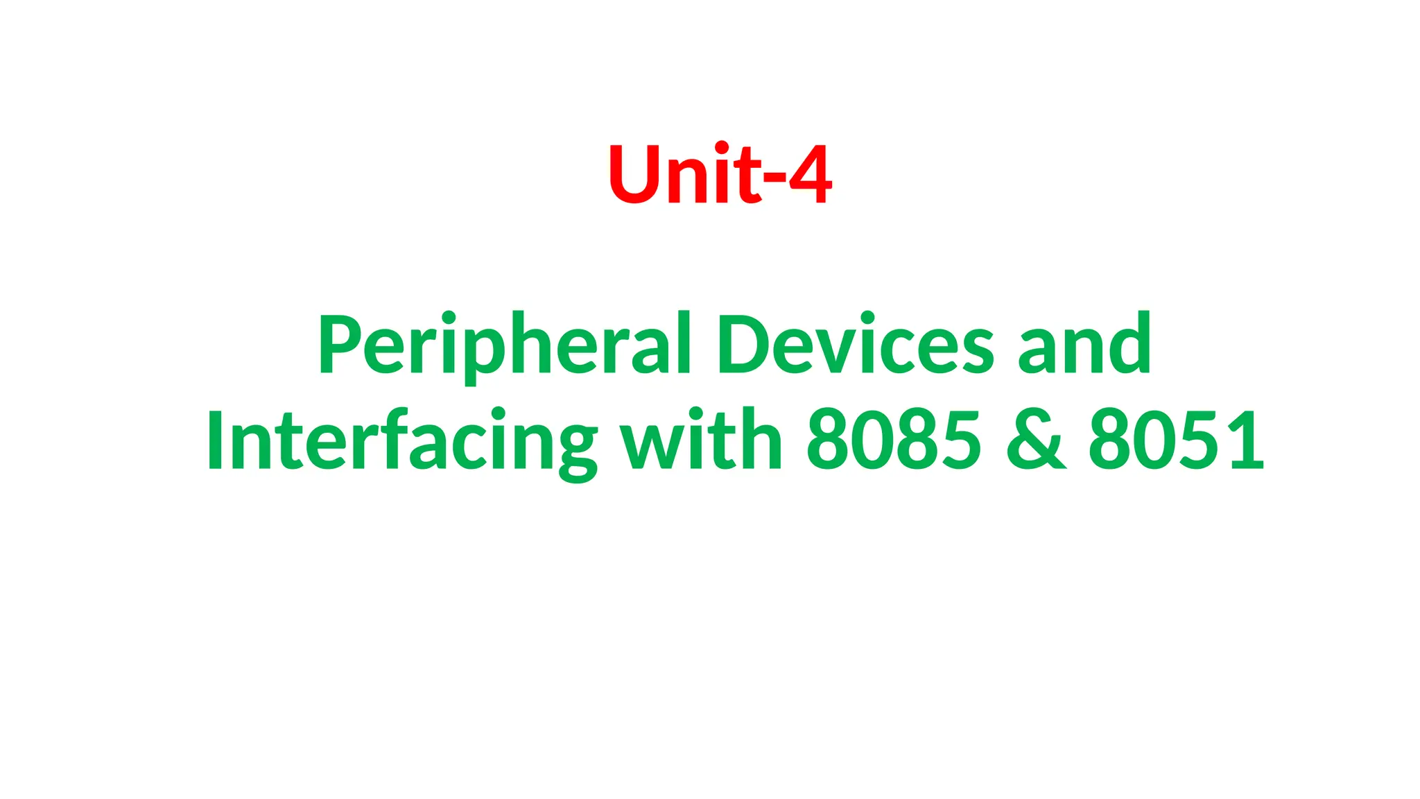
Peripheral Interfacing
• Peripheral
•It means various components or devices those are
connected to CPU.
• Actually these are input / output devices.
• Interfacing
• An interface is a concept that refers to a point of
interaction between objects or components and its
applicable level of both hardware and software.
4.
Contd..
• Microprocessor basedsystem design involves interfacing of
the processor with one or more peripheral devices.
• The purpose of communication with various input and
output devices connected to it.
• During the early days of the microprocessor revolution, these
techniques required complex hardware.
• It consisting of medium scale integration devices making the
design highly complex and time consuming.
5.
Contd..
• So, themanufacturers (INTEL) have developed a large
number of general and special purpose peripheral devices
most of them being single chip circuits.
• They are also programmable devices.
• Hence these peripheral devices are found to be of
tremendous use to a system designer.
6.
Types of PeripheralInterfacing
• Peripheral devices can broadly be classified into two
categories.
• General purpose peripherals
• Special purpose peripherals (Dedicated function
peripherals)
• General purpose peripheral devices that perform a task but
may be used for interfacing a variety of I/O devices to
microprocessor.
7.
Contd..
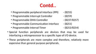
• Programmable peripheralInterface (PPI) - (8255)
• Programmable Interrupt Controller - (8259)
• Programmable DMA Controller - (8237/8257)
• Programmable Communication Interface - (8251)
• Programmable Interval Timer - (8253/8254)
• Special function peripherals are devices that may be used for
interfacing a microprocessor to a specific type of I/O device.
• These peripherals are more complex and therefore, relatively more
expensive than general purpose peripherals.
8.
Contd..
• Programmable CRTController
• Programmable Floppy Disc Controller
• Programmable Hard Disc Controller
• Programmable Keyboard and display interface.
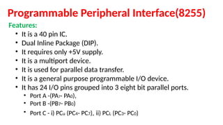
Programmable Peripheral Interface(8255)
Features:
•It is a 40 pin IC.
• Dual Inline Package (DIP).
• It requires only +5V supply.
• It is a multiport device.
• It is used for parallel data transfer.
• It is a general purpose programmable I/O device.
• It has 24 I/O pins grouped into 3 eight bit parallel ports.
• Port A -(PA7- PA0),
• Port B -(PB7- PB0)
• Port C - i) PCu (PC4- PC7), ii) PCL (PC3- PC0)
12.
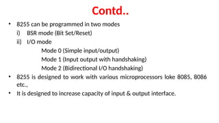
Contd..
• 8255 canbe programmed in two modes
i) BSR mode (Bit Set/Reset)
ii) I/O mode
Mode 0 (Simple input/output)
Mode 1 (Input output with handshaking)
Mode 2 (Bidirectional I/O handshaking)
• 8255 is designed to work with various microprocessors loke 8085, 8086
etc.,
• It is designed to increase capacity of input & output interface.
Contd..
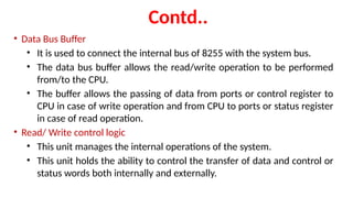
• Data BusBuffer
• It is used to connect the internal bus of 8255 with the system bus.
• The data bus buffer allows the read/write operation to be performed
from/to the CPU.
• The buffer allows the passing of data from ports or control register to
CPU in case of write operation and from CPU to ports or status register
in case of read operation.
• Read/ Write control logic
• This unit manages the internal operations of the system.
• This unit holds the ability to control the transfer of data and control or
status words both internally and externally.
15.
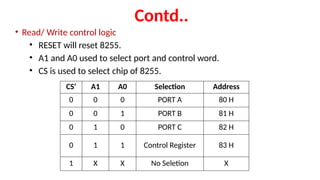
Contd..
• Read/ Writecontrol logic
• RESET will reset 8255.
• A1 and A0 used to select port and control word.
• CS is used to select chip of 8255.
CS’ A1 A0 Selection Address
0 0 0 PORT A 80 H
0 0 1 PORT B 81 H
0 1 0 PORT C 82 H
0 1 1 Control Register 83 H
1 X X No Seletion X
16.
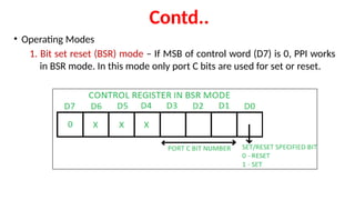
Contd..
• Operating Modes
1.Bit set reset (BSR) mode – If MSB of control word (D7) is 0, PPI works
in BSR mode. In this mode only port C bits are used for set or reset.
17.
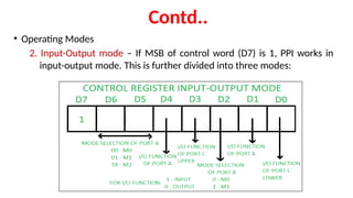
Contd..
• Operating Modes
2.Input-Output mode – If MSB of control word (D7) is 1, PPI works in
input-output mode. This is further divided into three modes:
18.
Contd..
• Operating Modes
•Mode 0
• In this mode all the three ports (port A, B, C) can work as simple
input function or simple output function.
• In this mode there is no interrupt handling capacity.
• Mode 1
• Handshake I/O mode or strobed I/O mode.
• In this mode either port A or port B can work as simple input port
or simple output port, and port C bits are used for handshake
signals before actual data transmission.
19.
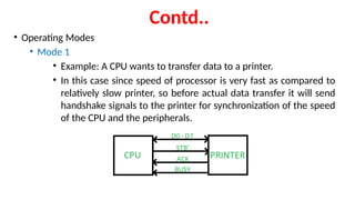
Contd..
• Operating Modes
•Mode 1
• Example: A CPU wants to transfer data to a printer.
• In this case since speed of processor is very fast as compared to
relatively slow printer, so before actual data transfer it will send
handshake signals to the printer for synchronization of the speed
of the CPU and the peripherals.
20.
Contd..
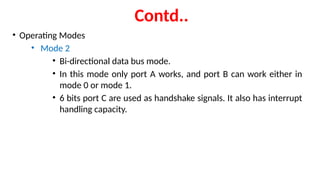
• Operating Modes
•Mode 2
• Bi-directional data bus mode.
• In this mode only port A works, and port B can work either in
mode 0 or mode 1.
• 6 bits port C are used as handshake signals. It also has interrupt
handling capacity.
21.
Contd..
• Applications
• LEDor Relay Interface
• Stepper Motor Interface
• Display Interface
• Keyboard Interface
• ADC or DAC Interface
• Traffic Signal Controller
• Lift Controller, etc.
22.
Puzzles
• A manstands on one side of a river, his dog on the other. The man calls his
dog, who immediately crosses the river without getting wet and without
using a bridge or a boat. How did the dog do it?
Answer: The river was frozen
• Turn me on my side and I am everything. Cut me in half and I am nothing.
What am I?
Answer: The number 8
• What has cities, but no houses; forests, but no trees; and water, but no
fish?
Answer: A Map
23.
Programmable DMA Controller(8257)
• In microprocessor based system, data transfer can be controlled by either
software or hardware. To transfer data microprocessor has to do the
following tasks
• Fetch the instruction
• Decode the instruction
• Execution of the instruction
• Microprocessor needs some amount of time to complete these tasks.
• But this data transfer is not suitable for large data transfer such as data
transfer from magnetic disk or optical disk to memory.
• In this situation hardware controlled data transfer technique is required.
24.
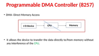
Programmable DMA Controller(8257)
• DMA- Direct Memory Access
• It allows the device to transfer the data directly to/from memory without
any interference of the CPU.
I/O Device CPU Memory
25.
Contd..
• DMA controllerwas designed by Intel, to have the fastest amongst all
the modes of data transfer rate with less processor utilization.
• Basically whenever an I/O device needs to transfer the data to the
memory, then it initially sends a request to DMA controller.
• On receiving data transfer request the controller sends HOLD request to
the CPU and waits for HLDA which is nothing but hold acknowledge by
the CPU.
26.
Contd..
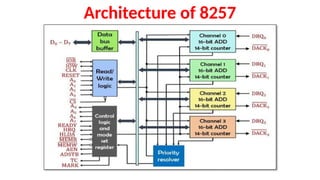
• Intel‘s 8257is a four channel DMA controller designed to be interfaced
with their family of microprocessors.
• Each channel can be independently programmable to transfer up to 64Kb
of data by DMA.
• Each channel can be independently perform read transfer, write transfer
and verify transfer.
Contd..
• Then themicroprocessor tri- states all the data bus, address bus, and
control bus. The CPU leaves the control over bus and acknowledges the
HOLD request through HLDA signal.
• Now the CPU is in HOLD state and the DMA controller has to manage the
operations over buses between the CPU, memory, and I/O devices.
• The chip support four DMA channels, i.e. four peripheral devices can
independently request for DMA data transfer through these channels at a
time.
29.
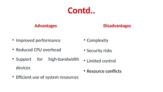
Contd..
Advantages
• Improved performance
•Reduced CPU overhead
• Support for high-bandwidth
devices
• Efficient use of system resources
Disadvantages
• Complexity
• Security risks
• Limited control
• Resource conflicts
30.
Puzzles
• Four carscome to a four-way stop, all coming from a different direction.
They can't decide who got there first, so they all go forward at the same
time. They do not crash into each other, but all four cars go. How is this
possible?
Answer: They all made right-hand turns
• What is made of water but if you put it into water it will die?
Answer: An ice cube
31.
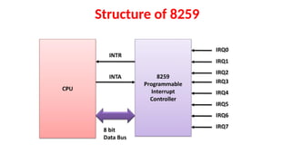
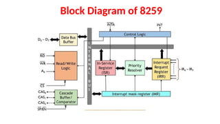
Programmable Interrupt Controller(8259)
• The most desirable method is that the microprocessor can execute its
main program and only stop to service peripheral devices when CPU
receives a signal from the device itself.
• Then the processor should complete whatever instruction is currently
being executed and fetch a new routine that will service the requesting
device.
• However, after completion of service, the processor would resume exactly
where it left off. This method is known as interrupt.
• When the number of I/O devices are less, the already available inter
rupts
of microprocessors are sufficient.
32.
Contd..
• The microprocessorhas limited hardware interrupts with limited interrupt
priority.
• To overcome all difficulties, a Programmable Interrupt Controller (PIC) has
been designed and can be used to handle many interrupts at a time.
• The Programmable Interrupt Controller (PIC) functions as an overall
manager in an interrupt-driven system environment.
• The 8259 Programmable Interrupt Controller can be interfaceable with
8085, 8086 and 8088 processors.
33.
Features of 8259
•Intel 8259 is designed for Intel 8085 and Intel 8086 microprocessor.
• It can be programmed either in level triggered or in edge triggered
interrupt level.
• This device is an eight-level priority controller.
• We can mask individual bits of interrupt request register.
• Programmable interrupt modes.
• Single a +5 V supply (no clocks).
• Available in 28-pin DIP and 28-lead.
• We can increase interrupt handling capability upto 64 interrupt level by
cascading further 8259 PICs.
• Clock cycle is not required.
Advantages of 8259
•Interrupt Management: The 8259 PIC is designed to handle interrupts
efficiently and effectively, allowing for faster and more reliable processing
of interrupts in a system.
• Flexibility: The 8259 PIC is programmable, meaning that it can be
customized to suit the specific needs of a given system, including the
number and type of interrupts that need to be managed.
• Compatibility: The 8259 PIC is compatible with a wide range of
microprocessors, making it a popular choice for managing interrupts in
many different systems.
• Multiple Interrupt Inputs: The 8259 PIC can manage up to 8 interrupt
inputs, allowing for the management of complex systems with multiple
37.
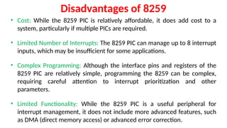
Disadvantages of 8259
•Cost: While the 8259 PIC is relatively affordable, it does add cost to a
system, particularly if multiple PICs are required.
• Limited Number of Interrupts: The 8259 PIC can manage up to 8 interrupt
inputs, which may be insufficient for some applications.
• Complex Programming: Although the interface pins and registers of the
8259 PIC are relatively simple, programming the 8259 can be complex,
requiring careful attention to interrupt prioritization and other
parameters.
• Limited Functionality: While the 8259 PIC is a useful peripheral for
interrupt management, it does not include more advanced features, such
as DMA (direct memory access) or advanced error correction.
38.
Puzzles
• A womanshoots her husband. Then she holds him underwater for over 5
minutes. Finally, she hangs him. But 5 minutes later they both go out
together and enjoy a wonderful dinner together. How can this be?
Answer: The woman was a photographer. She shot a picture of her husband,
developed it, and hung it up to dry.
• How can 8 + 8 = 4?
Answer : When you think in terms of time. 8 AM + 8 hours= 4 o’clock.
39.
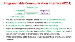
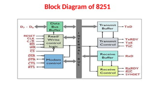
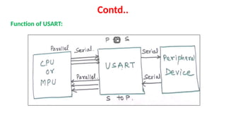
Programmable Communication Interface(8251)
Transfer Data
Receive Data
8 bit, 16 bit, 32 bit….
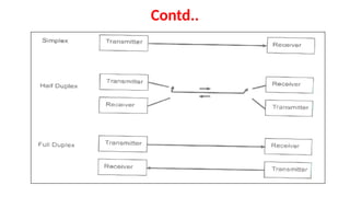
• The data transmission happens either parallel or serial transmission.
• In parallel transmission the data transmission at the same time.
• In serial transmission the data transmission one after other.
• When the microprocessor transmitting the data over a long distance it will
request series transmission because number of lines connected in parallel
transmission between microprocessor and peripheral device.
• While transmitting data through a long distance there are chances errors
can occur.
Micropro
cessor
Peripheral
Devices
40.
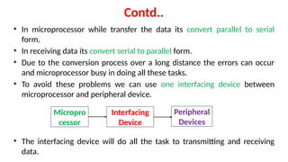
Contd..
• In microprocessorwhile transfer the data its convert parallel to serial
form.
• In receiving data its convert serial to parallel form.
• Due to the conversion process over a long distance the errors can occur
and microprocessor busy in doing all these tasks.
• To avoid these problems we can use one interfacing device between
microprocessor and peripheral device.
• The interfacing device will do all the task to transmitting and receiving
data.
Micropro
cessor
Peripheral
Devices
Interfacing
Device
41.
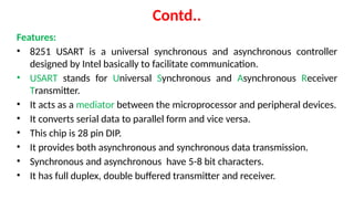
Contd..
Features:
• 8251 USARTis a universal synchronous and asynchronous controller
designed by Intel basically to facilitate communication.
• USART stands for Universal Synchronous and Asynchronous Receiver
Transmitter.
• It acts as a mediator between the microprocessor and peripheral devices.
• It converts serial data to parallel form and vice versa.
• This chip is 28 pin DIP.
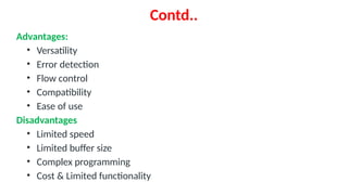
• It provides both asynchronous and synchronous data transmission.
• Synchronous and asynchronous have 5-8 bit characters.
• It has full duplex, double buffered transmitter and receiver.
Puzzles
• A redhouse is made from red bricks. A blue house is made from blue bricks. A yellow
house is made from yellow bricks. What is a greenhouse made from?
Answer: Glass
• There is a word in the English language in which the first two letters signify a male, the
first three letters signify a female, the first four signify a great man, and the whole
word, a great woman. What is the word?
Answer: Heroine
• First I am dried, then I am wet. The longer I swim, the more taste you get. What am I?
Answer: Tea
47.
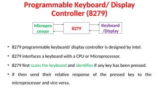
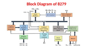
Programmable Keyboard/ Display
Controller(8279)
• 8279 programmable keyboard/ display controller is designed by intel.
• 8279 interfaces a keyboard with a CPU or Microprocessor.
• 8279 first scans the keyboard and identifies if any key has been pressed.
• If then send their relative response of the pressed key to the
microprocessor and vice versa.
Micropro
cessor
Keyboard
/Display
8279
48.
Contd..
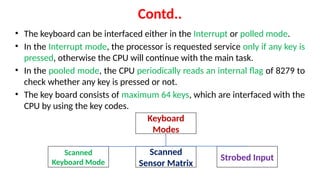
• The keyboardcan be interfaced either in the Interrupt or polled mode.
• In the Interrupt mode, the processor is requested service only if any key is
pressed, otherwise the CPU will continue with the main task.
• In the pooled mode, the CPU periodically reads an internal flag of 8279 to
check whether any key is pressed or not.
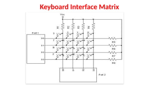
• The key board consists of maximum 64 keys, which are interfaced with the
CPU by using the key codes.
Keyboard
Modes
Scanned
Keyboard Mode
Scanned
Sensor Matrix
Strobed Input
49.
Contd..
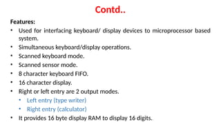
Features:
• Used forinterfacing keyboard/ display devices to microprocessor based
system.
• Simultaneous keyboard/display operations.
• Scanned keyboard mode.
• Scanned sensor mode.
• 8 character keyboard FIFO.
• 16 character display.
• Right or left entry are 2 output modes.
• Left entry (type writer)
• Right entry (calculator)
• It provides 16 byte display RAM to display 16 digits.
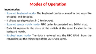
Modes of Operation
Inputmodes:
• Scanned keyboard mode- The keyboard can be scanned in two ways like
encoded and decoded.
• It allows key depressions in 2 key lockout.
• Scanned sensor matrix mode- FIFO buffer is converted into 8x8 bit map.
• Each bit represents the state of the switch at the same location in the
keyboard matrix.
• Strobed input mode- The data is entered into the FIFO RAM from the
return lines at the rising edge of the CNTL/STB signal.
Puzzles
• Michelle’s momhas four children. The first child is named April, the
second is named May and the third is named June. What is the name of
her fourth child?
Answer: Michelle
54.
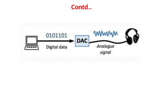
Interfacing Analog toDigital & Digital to Analog
Converter
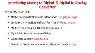
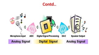
Why is ADC important?
• All the microcontrollers store information using digital logic.
• Compress information to digital form for efficient storage.
• Medium for storing digital data is more robust.
• Digital data transfer is more efficient.
• Digital data is easily reproducible.
• Provides a link between real world signals and data storage.
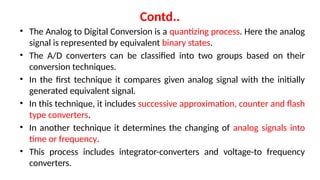
Contd..
• The Analogto Digital Conversion is a quantizing process. Here the analog
signal is represented by equivalent binary states.
• The A/D converters can be classified into two groups based on their
conversion techniques.
• In the first technique it compares given analog signal with the initially
generated equivalent signal.
• In this technique, it includes successive approximation, counter and flash
type converters.
• In another technique it determines the changing of analog signals into
time or frequency.
• This process includes integrator-converters and voltage-to frequency
converters.
58.
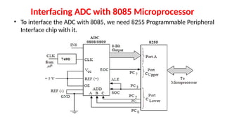
Interfacing ADC with8085 Microprocessor
• To interface the ADC with 8085, we need 8255 Programmable Peripheral
Interface chip with it.
59.
Contd..
• The PortA of 8255 chip is used as the input port.
• The PC7 pin of Port Cupper is connected to the End of Conversion (EOC)
Pin of the analog to digital converter.
• This port is also used as input port.
• The lower port is used as output port. The PC2-0 lines are connected to
three address pins of this chip to select input channels.
• The PC3 pin is connected to the Start of Conversion (SOC) pin and ALE
pin of ADC 0808/0809.
60.
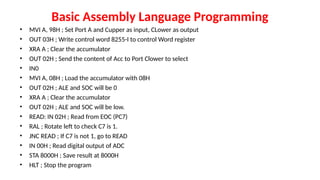
Basic Assembly LanguageProgramming
• MVI A, 98H ; Set Port A and Cupper as input, CLower as output
• OUT 03H ; Write control word 8255-I to control Word register
• XRA A ; Clear the accumulator
• OUT 02H ; Send the content of Acc to Port Clower to select
• IN0
• MVI A, 08H ; Load the accumulator with 08H
• OUT 02H ; ALE and SOC will be 0
• XRA A ; Clear the accumulator
• OUT 02H ; ALE and SOC will be low.
• READ: IN 02H ; Read from EOC (PC7)
• RAL ; Rotate left to check C7 is 1.
• JNC READ ; If C7 is not 1, go to READ
• IN 00H ; Read digital output of ADC
• STA 8000H ; Save result at 8000H
• HLT ; Stop the program
61.
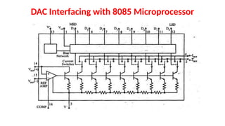
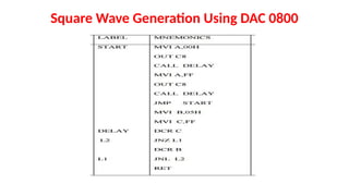
DAC Interfacing with8085 Microprocessor
DAC 0800 Features
• To convert the digital signal to analog signal a Digital-to-Analog
Converter (DAC) has to be employed.
• The DAC will accept a digital (binary) input and convert to analog voltage
or current.
• Every DAC will have "n" input lines and an analog output.
• The DAC require a reference analog voltage (Vref) or current (Iref)
source.
• The smallest possible analog value that can be represented by the n-bit
binary code is called resolution.
62.
DAC Interfacing with8085 Microprocessor
• The resolution of DAC with n-bit binary input is ½ of reference analog
value.
• The DAC0800 is an 8-bit, high speed, current output DAC with a typical
settling time (conversion time) of 100 ns.
• It produces complementary current output, which can be converted to
voltage by using simple resistor load.
• The DAC0800 require a positive and a negative supply voltage in the
range of ± 5V to ±18V.
Puzzles
• Before thedays of motor cars, a man rode into town on his horse. He
arrived on Sunday, spent three days in town and left on Sunday. How is
that possible?
Answer : The name of the horse was Sunday.
• A man drove his Innova car all the way from Shimla to Delhi only to
discover at the end of the trip that he had a punctured tyre from the
very start. Yet his Innova car was not at all affected by it? How is this
possible?
Answer : Punctured tyre must be a spare tyre.