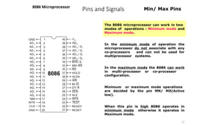
Module 1
Introduction to Microprocessor and
Computer
What is used in CPU?
• Program controlled semiconductor device (IC) which fetches (from
memory), decodes and executes instructions.
• It is used as CPU (Central Processing Unit) in computers.
Microprocessor
Generation
First Generation
Between 1971 – 1973
PMOS technology, non compatible with TTL
4 bit processors  16 pins
8 and 16 bit processors  40 pins
Due to limitations of pins, signals are
multiplexed
Second Generation
During 1973
NMOS technology  Faster speed, Higher
density, Compatible with TTL
4 / 8/ 16 bit processors  40 pins
Ability to address large memory spaces
and I/O ports
Greater number of levels of subroutine
nesting
Better interrupt handling capabilities
Intel 8085 (8 bit processor)
Third Generation
During 1978
HMOS technology  Faster speed, Higher
packing density
16 bit processors  40/ 48/ 64 pins
Easier to program
Dynamically relatable programs
Processor has multiply/ divide arithmetic
hardware
More powerful interrupt handling
capabilities
Flexible I/O port addressing
Intel 8086 (16 bit processor)
Fourth Generation
During 1980s
Low power version of HMOS technology
(HCMOS)
32 bit processors
Physical memory space 224
bytes = 16 Mb
Virtual memory space 240
bytes = 1 Tb
Floating point hardware
Supports increased number of addressing
modes
Intel 80386
Fifth Generation Pentium
3
Functional blocks
Microprocessor
Flag
Register
Timing and
control unit
Register array or
internal memory
Instruction
decoding unit
PC/ IP
ALU
Control Bus Address Bus
Data Bus
4
Computational Unit;
performs arithmetic and
logic operations
Various conditions of the
results are stored as
status bits called flags in
flag register
Internal storage of data
Generates the
address of the
instructions to be
fetched from the
memory and send
through address
bus to the
memory
Decodes instructions; sends
information to the timing and
control unit
Generates control signals for
internal and external operations
of the microprocessor
Overview
8086 Microprocessor
First 16- bit processor released by
INTEL in the year 1978
Originally HMOS, now manufactured
using HMOS III technique
Approximately 29, 000 transistors, 40
pin DIP, 5V supply
Does not have internal clock; external
asymmetric clock source with 33%
duty cycle
20-bit address to access memory  can
address up to 220
= 1 megabytes of
memory space.
Addressable memory space is
organized in to two banks of 512 kb
each; Even (or lower) bank and Odd (or
higher) bank. Address line A0 is used to
select even bank and control signal
is used to access odd bank
Uses a separate 16 bit address for I/O
mapped devices  can generate 216
=
64 k addresses.
Operates in two modes: minimum mode
and maximum mode, decided by the
signal at MN and pins.
Internal Architecture of Microprocessor 8086
Execution Unit (EU)
EU executes instructions that have
already been fetched by the BIU.
BIU and EU functions separately.
Bus Interface Unit (BIU)
BIU fetches instructions, reads data from
memory and I/O ports, writes data to
memory and I/ O ports.
The Execution Unit (EU)
• Control circuitry
• Instruction Decoder
• The ALU
• Flag /Status registers
• General Purpose Registers
The main
components of
the EU are:
Control Circuitry, Instruction Decoder And
ALU:
• The EU contains control circuit which directs internal operations.
• Fetches instructions from the Queue in BIU, decodes and executes
arithmetic and logic operations using the ALU.
• Sends control signals for internal data transfer operations within the
microprocessor.
• Sends request signals to the BIU to access the external module.
• It operates with respect to T-states (clock cycles) and not machine
cycles.
Flag /Status Register
The flag register, 6 out of 9 flags are used as status flags.
When the microprocessor performs an arithmetic or logical
operation in ALU, then depending upon the status of the
result, the microprocessor will store corresponding status bits
0 or 1 in status flags.
The status flags are,
• Carry flag (CF)
• Parity flag (PF)
• Auxiliary carry flag (AF)
• Zero flag (ZF)
• Sign flag (SF), and
• Overflow flag (OF).
Control Flags :
• Depending upon the value of the controlling flag bit, the
microprocessor will control a particular operation i.e., these
flags are used to control certain operations. There are three
controlling flags namely,
• Interrupt flag (IF),
• Direction flag (DF), and
• Trap flag (TP).
Registers
General-purpose registers are used to store temporary data within the
microprocessor. There are 4 general-purpose registers and 4 special purpose
register are there in the 8086 microprocessor.
General Purpose Register
• AX register: This is the accumulator. It is of 16 bits and is divided into two 8-bit registers AH and AL to also
perform 8-bit instructions. It is generally used for arithmetical and logical instructions .
• BX register: The base register. It is of 16 bits and is divided into two 8-bit registers BH and BL to also
perform 8-bit instructions. It is used to store the value of the offset.
Example: MOV BL, [500] (BL = 500H)
• CX register: Counter register. It is of 16 bits and is divided into two 8-bit registers CH and CL to
also perform 8-bit instructionsIt holds count for instructions like loop, rotate, shift and string
operations.
Example:
• DX register: Data register. It is of 16 bits and is divided into two 8-bit registers DH and DL to also
perform 8-bit instructions. It is used with AX to hold 32 bit values during multiplication and division.
MOV CX, 0005 LOOP
Special purpose Register
• SP: This is the stack pointer. It is of 16 bits. It points to the topmost item of the
stack. If the stack is empty the stack pointer will be (FFFE)H. Its offset address is
relative to the stack segment.
• BP :This is the base pointer. It is of 16 bits. It is primarily used in accessing
parameters passed by the stack. Its offset address is relative to the stack segment.
• SI :This is the source index register. It is of 16 bits. It is used in the pointer
addressing of data and as a source in some string-related operations. Its offset is
relative to the data segment.
• DI :This is the destination index register. It is of 16 bits. It is used in the pointer
addressing of data and as a destination in some string-related operations. Its
offset is relative to the extra segment.
BIU
Contains
• 4 Segment registers
• The Instruction Pointer
• A prefetch queue
• Address Generation Circuit.
1. The Bus Interface Unit (BIU)
• It provides the interface of 8086 to external memory and I/O devices
via the System Bus.
• It performs various machine cycles such as memory read, I/O read
etc. to transfer data between memory and I/O devices.
• BIU performs the following functions-
• It generates the 20 bit physical address for memory access.
• It fetches instructions from the memory.
• It transfers data to and from the memory and I/O.
• Maintains the 6 byte prefetch instruction queue(supports pipelining).
Instruction Pointer (IP)
• It is a 16 bit register. It holds offset of the next instructions in the Code
Segment.
• IP is incremented after every instruction byte is fetched.
• IP gets a new value whenever a branch instruction occurs.
• CS is multiplied by 10H to give the 20 bit physical address of the Code
Segment.
• Address of the next instruction is calculated as CS x 10H + IP.
Example:
• CS = 4321H IP = 1000H, then CS x 10H = 43210H + offset = 44210H
• This is the address of the instruction.
SEGMENT REGISTER
Code Segment
register:
CS holds the base
address for the Code
Segment. All programs
are stored in the Code
Segment and accessed
via the IP.
Data Segment
register:
DS holds the base
address for the Data
Segment
Stack Segment
register:
SS holds the base
address for the Stack
Segment
Extra Segment
register:
ES holds the base
address for the Extra
Segment.
Address Generation Circuit
• The BIU has a Physical Address Generation Circuit.
• It generates the 20 bit physical address using Segment and Offset
addresses using the formula:
• Physical Address = Segment Address x 10H + Offset Address
6 Byte Pre-fetch Queue
• It is a 6 byte queue (FIFO).
• Fetching the next instruction (by BIU from CS) while executing the
current instruction is called pipelining.
• Gets flushed whenever a branch instruction occurs.
BUS CLOCK CYCLE:
• Bus cycle corresponds to a sequence of events that starts
with an address being output on system address bus
followed by a write or read data transfer.
• During these operations, a series of control signals are also
produced by microprocessor to control direction and timing
of bus.
• There are at least four clock periods in a bus cycle of 8086
microprocessor. These four clock periods are called T1, T2,
T3 and T4 states. These four clock states gives bus cycle
duration T of 200 ns *4 = 800 ns in 5-MHz 8086 system.
• Read Cycle : When a read cycle is to be performed, during
T1 microprocessor puts an address on address bus, and then
bus is put in high impedance state during T2 state. Data to
be read must be out on bus during T3 and T4. During T3 bus
is made “reserved for data in” and finally data is read during
T4.
• Write Cycle : In case of write memory cycle, during T1 state
microprocessor puts an address on address bus. Data is put
on data bus by CPU during T2 state and maintained during
T3 and T4 states, that is written out to memory or I/O devices.
PINS AND SIGNALS
The pins and signals of 8086 can be
classified into six groups, they are as
follows.
• Address/status bus
• Address/data bus
• Control and status signals
• Interrupts and external initiated
signals
• Power supply and clock frequency
signals
Address/data bus
• AD0-AD15. These are 16 address/data bus. AD0-AD7 carries low order
byte data and AD8-AD15 carries higher order byte data. During the
first clock cycle, it carries 16-bit address and after that it carries 16-bit
data.
Address/status bus
• A16-A19/S3-S6. A16-A19: High order address bus. These are
multiplexed with status signals.
• Time shared address I/O operation. These are the 4 address/status
buses. During the first clock cycle, it carries 4-bit address and later it
carries status signals. Information is updated at the start of each clock
and available on status pin s5
S4 S3 CHARACTERISTICS
0 0 EXTRA SEGMENT ACCESS
0 1 STACK SEGMENT
1 0 CODE SEGMENT
1 1 DATA SEGMENT
Pins and Signals
8086 Microprocessor
28
Common signals
BHE (Active Low)/S7 (Output)
Bus High Enable/Status
It is used to enable data onto the most
significant half of data bus, D8-D15. 8-bit
device connected to upper half of the
data bus use BHE (Active Low) signal. It
is multiplexed with status signal S7.
MN/ MX
MINIMUM / MAXIMUM
This pin signal indicates what mode the
processor is to operate in.
RD (Read) (Active Low)
The signal is used for read operation.
It is an output signal.
It is active when low.
Pins and Signals
8086 Microprocessor
29
TEST
input is tested by the ‘WAIT’ instruction.
8086 will enter a wait state after
execution of the WAIT instruction and
will resume execution only when the is
made low by an active hardware.
This is used to synchronize an external
activity to the processor internal
operation.
READY
This is the acknowledgement from the
slow device or memory that they have
completed the data transfer.
The signal made available by the devices
is synchronized by the 8284A clock
generator to provide ready input to the
8086.
The signal is active high.
Pins and Signals
8086 Microprocessor
30
RESET (Input)
Causes the processor to immediately
terminate its present activity.
The signal must be active HIGH for at
least four clock cycles.
CLK
The clock input provides the basic timing
for processor operation and bus control
activity. Its an asymmetric square wave
with 33% duty cycle.
INTR Interrupt Request
This is a triggered input. This is sampled
during the last clock cycles of each
instruction to determine the availability
of the request. If any interrupt request is
pending, the processor enters the
interrupt acknowledge cycle.
This signal is active high and internally
synchronized.
Pins and Signals
8086 Microprocessor
31
Min/ Max Pins
The 8086 microprocessor can work in two
modes of operations : Minimum mode and
Maximum mode.
In the minimum mode of operation the
microprocessor do not associate with any
co-processors and can not be used for
multiprocessor systems.
In the maximum mode the 8086 can work
in multi-processor or co-processor
configuration.
Minimum or maximum mode operations
are decided by the pin MN/ MX(Active
low).
When this pin is high 8086 operates in
minimum mode otherwise it operates in
Maximum mode.
Pins and Signals
8086 Microprocessor
Pins 24 -31
For minimum mode operation, the MN/ is tied to
VCC (logic high)
8086 itself generates all the bus control signals
DT/ (Data Transmit/ Receive) Output signal from the
processor to control the direction of data flow
through the data transceivers
(Data Enable) Output signal from the processor
used as out put enable for the transceivers
ALE (Address Latch Enable) Used to demultiplex the
address and data lines using external latches
M/ Used to differentiate memory access and I/O
access. For memory reference instructions, it is
high. For IN and OUT instructions, it is low.
Write control signal; asserted low Whenever
processor writes data to memory or I/O port
(Interrupt Acknowledge) When the interrupt
request is accepted by the processor, the output is
low on this line.
Minimum mode signals
Pins and Signals
8086 Microprocessor
HOLD Input signal to the processor form the bus masters
as a request to grant the control of the bus.
Usually used by the DMA controller to get the
control of the bus.
HLDA (Hold Acknowledge) Acknowledge signal by the
processor to the bus master requesting the control
of the bus through HOLD.
The acknowledge is asserted high, when the
processor accepts HOLD.
33
Minimum mode signals
Pins 24 -31
For minimum mode operation, the MN/ is tied to
VCC (logic high)
8086 itself generates all the bus control signals
Pins and Signals
8086 Microprocessor
During maximum mode operation, the MN/ is
grounded (logic low)
Pins 24 -31 are reassigned
, , Status signals; used by the 8086 bus controller to
generate bus timing and control signals. These are
decoded as shown.
34
Maximum mode signals
Pins and Signals
8086 Microprocessor
During maximum mode operation, the MN/ is
grounded (logic low)
Pins 24 -31 are reassigned
, (Queue Status) The processor provides the status
of queue in these lines.
The queue status can be used by external device to
track the internal status of the queue in 8086.
The output on QS0 and QS1 can be interpreted as
shown in the table.
35
Maximum mode signals
Pins and Signals
8086 Microprocessor
During maximum mode operation, the MN/ is
grounded (logic low)
Pins 24 -31 are reassigned
, (Bus Request/ Bus Grant) These requests are used
by other local bus masters to force the processor
to release the local bus at the end of the
processor’s current bus cycle.
These pins are bidirectional.
The request on will have higher priority than
An output signal activated by the LOCK prefix
instruction.
Remains active until the completion of the
instruction prefixed by LOCK.
The 8086 output low on the pin while executing an
instruction prefixed by LOCK to prevent other bus
masters from gaining control of the system bus.
Maximum mode signals
MINIMUM AND MAXIMUM MODES
Minimum Mode 8086 System
• The 8086 microprocessor operates in minimum mode when MN/MX’ = 1.
• In minimum mode,8086 is the only processor in the system which provides all
the control signals which are needed for memory operations and I/O interfacing.
• Here the circuit is simple but it does not support multiprocessing.
• The other components which are transceivers, latches, 8284 clock generator,
74138 decoder, memory and i/o devices are also present in the system.
• The address bus of 8086 is 20 bits long. By this we can access 220
byte memory
i.e. 1MB . Out of 20 bits, 16 bits A0 to A15(or 16 lines) are multiplexed with a data
bus. By multiplexing, it means they will act as address lines during the first T
state of the machine cycle and in the rest, they act as data lines. A16 to A19 are
multiplexed S3 to S6 and BHE’ is multiplexed with S7.
40
8282 (8 bits) latch :
The latches are buffered D FF. They are used to
separate the valid address from the multiplexed
Address/data bus by using the control signal ALE,
which is connected to strobe(STB) of 8282. The
ALE is active high signal. Here three such latches
are required because the address is 20 bits.
8286 (8 bits) transceivers :
They are bidirectional buffers and also known as
data amplifiers. They are used to separate the valid
data from multiplexed add/data bus. Two such
transceivers are needed because the data bus is 16
bits long. 8286 is connected to DT/R’ and DEN’
signals. They are enabled through the DEN
signal .The direction of data on the data bus is
controlled by the DT/R’ signal. DT/R’ is connected
to T and DEN’ is connected to OE’.
41
•8284 clock generator is used to provide the clock
used to synchronize process.
74138 3:8 decoder.
•M/IO’= 1,then I/O transfer is performed over the
bus. and when M/IO’ = 0, then I/O operation is
performed.
•The signals RD’ and write WR’ are used to identify
whether a read bus cycle or a write bus cycle is
performing. When WR’ = 0 ,then it indicates that
valid output data on the data bus.
•RD’ indicates that the 8086 is performing a read
data or instruction fetch process is occurring .During
read operations, one other control signal is also
used, which is DEN ( data enable) and it indicates the
external devices when they should put data on the
bus.
•Control signals for all operations are generated by
decoding M/IO’, RD’, WR’. They are decoded by
•INTR and INTA :
When INTR = 1,then there is an
interrupt to 8086 by other
devices for their service. When
INTA’= 0,then it indicates that
the processor is ready to
service them.
•HOLD and HLDA :
•The bus request is made by
other devices using the HOLD
signal and the processor
acknowledges them using the
HLDA output signal.
Minimum Code Read Cycle timing diagram
• At T1 state ALE =1 ,this indicates that a valid address is latched
on the address bus and also M / IO’= 1, which indicates the
memory operation is in progress.
• In T2, the address is removed from the local bus and is sent to
the addressed device. Then the bus is tristated.
• When RD’ = 0 , the valid data is present on the data bus.
• During T2 DEN’ =0, which enables transceivers and DT/R’ =
0 ,which indicates that the data is received.
• During T3, data is put on the data bus and the processor reads it.
• The output device makes the READY line high. This means the
output device has performed the data transfer process. When
the processor makes the read signal to 1, then the output device
will again tristate its bus drivers.
Write memory cycle
45
•At T1 state ALE =1 ,this indicates that a valid address is latched on the
address bus and also M / IO’= 1, which indicates the memory operation
is in progress.
•In T2, the processor sends the data to be written to the addressed
location.
•The data is buffered on the bus until the middle of T4 state.
•The WR’=0 becomes at the beginning of T2.
•The BHE’ and A0 signals are used to select the byte or bytes of memory
or I/O word.
•During T2 DEN’ =0, which enables, transceivers and DT/R’ = 1 ,which
indicates that the data is transferred by the processor to the addressed
device.
All kinds of memory and i/o operations are performed using the
decoding of M/IO’ and RD’ WR’ .
47
Maximum Mode 8086 System
48
•In this we can connect more
processors to 8086 (8087/8089).
•8086 max mode is basically for
implementation of allocation of global
resources and passing bus control to
other coprocessor(i.e. second
processor in the system), because two
processors can not access system bus
at same instant.
•All processors execute their own
program.
•The resources which are common to
all processors are known as global
resources.
•The resources which are allocated to
a particular processor are known as
local or private resources.
49
•When MN/ MX’ = 0 , 8086 works in max
mode.
•Clock is provided by 8284 clock generator.
•8288 bus controller- Address form the
address bus is latched into 8282 8-bit latch.
Three such latches are required
because address bus is 20 bit. The ALE(Address
latch enable) is connected to STB(Strobe) of
the latch. The ALE for latch is given by 8288
bus controller.
•The data bus is operated through 8286 8-bit
transceiver. Two such transceivers are required,
because data bus is 16-bit. The transceivers
are enabled the DEN signal, while the
direction of data is controlled by the DT/R
signal. DEN is connected to OE’ and DT/ R’ is
connected to T. Both DEN and DT/ R’ are given
by 8288 bus controller.
Control signals for all
operations are generated by
decoding S’2, S’1 and S’0 using
8288 bus controller.
•Bus request is done using RQ’ / GT’ lines
interfaced with 8086. RQ0/GT0 has more priority
than RQ1/GT1.
•INTA’ is given by 8288, in response to an
interrupt on INTR line of 8086.
•In max mode, the advanced write signals get
enabled one T-state in advance as compared to
normal write signals. This gives slower devices
more time to get ready to accept the data,
therefore it reduces the number of cycles.
Read Cycle for Max Mode
Write cycle for Max Mode
53
Group I : Addressing modes for register and
immediate data
Group IV : Relative Addressing mode
Group V : Implied Addressing mode
Group III : Addressing modes for I/O ports
Group II : Addressing modes for memory data
Addressing Modes
54
8086 Microprocessor
Every instruction of a program has to operate on a data.
The different ways in which a source operand is denoted
in an instruction are known as addressing modes.
1. Register Addressing
2. Immediate Addressing
3. Direct Addressing
4. Register Indirect Addressing
5. Based Addressing
6. Indexed Addressing
7. Based Index Addressing
8. String Addressing
9. Direct I/O port Addressing
10. Indirect I/O port Addressing
11. Relative Addressing
12. Implied Addressing
1.REGISTER ADDRESSING
• The instruction will specify the name of the register which holds the data
to be operated by the instruction.
Example:
MOV CL, DH
• The content of 8-bit register DH is moved to another 8-bit register CL
• (CL)  (DH)
Immediate Addressing
• In immediate addressing mode, an 8-bit or 16-bit data is specified as part of the
instruction
Example:
MOV DL, 08H
The 8-bit data (08H) given in the instruction is moved to DL
(DL)  08H
MOV AX, 0A9FH
The 16-bit data (0A9FH) given in the instruction is moved to AX register
(AX)  0A9FH
Addressing Modes : Memory Access
57
8086 Microprocessor
Physical Address (20 Bits)
Adder
Segment Register (16 bits) 0 0 0 0
Offset Value (16 bits)
Segment and offset: ( OFF SET – Logical Adress)
Segment Offset within a program, all memory locations within a segment are relative to the
segment starting address. The distance in bytes from the segment address to another location
within the segment is expressed as an offset (or displacement)
Addressing Modes : Memory Access
8086 Microprocessor
20 Address lines  8086 can address up to 220
= 1M bytes of
memory
However, the largest register is only 16 bits
Physical Address will have to be calculated Physical Address : Actual
address of a byte in memory. i.e. the value which goes out onto the
address bus.
Memory Address represented in the form – Seg : Offset (Eg -
89AB:F012)
Each time the processor wants to access memory, it takes the contents of
a segment register, shifts it one hexadecimal place to the left (same as
multiplying by 1610), then add the required offset to form the 20- bit
address
89AB : F012  89AB  89AB0 (Paragraph to byte  89AB x 10 = 89AB0)
F012  0F012 (Offset is already in byte unit)
+ -------
98AC2 (The absolute address)
16 bytes of contiguous
memory
Addressing Modes : Memory Access
8086 Microprocessor
To access memory we use these four registers: BX,
SI, DI, BP
Combining these registers inside [ ] symbols, we can
get different memory locations (Effective Address,
EA)
Supported combinations:
[BX + SI]
[BX + DI]
[BP + SI]
[BP + DI]
[SI]
[DI]
d16 (variable offset only)
[BX]
[BX + SI + d8]
[BX + DI + d8]
[BP + SI + d8]
[BP + DI + d8]
[SI + d8]
[DI + d8]
[BP + d8]
[BX + d8]
[BX + SI + d16]
[BX + DI + d16]
[BP + SI + d16]
[BP + DI + d16]
[SI + d16]
[DI + d16]
[BP + d16]
[BX + d16]
BX
BP
SI
DI
+ disp
Accessing data from commonly used I/O mapped devices or
ports is done using these addressing modes.
Example
IN AL,
[09H]
PORT adder = 09H (AL) ← (PORT)
The content of the port with address 09H is moved to the AL register
Input/Output
Mode
Relative addressing mode
• In this addressing mode, the effective address of a program instruction is specified
relative to Instruction Pointer (IP) by an 8-bit signed displacement.
Example: JZ 0AH
Operations:
000AH  0AH (sign extend)
If ZF = 1, then
EA = (IP) + 000AH
BA = (CS) x 1610
MA = BA + EA
If ZF = 1, then the program control jumps to new address calculated above.
If ZF = 0, then next instruction of the program is executed.
Implied Addressing
• Inbuilt Instructions
• Instructions using this mode have no operands. The instruction itself
will specify the data to be operated by the instruction.
• Example: CLC
• This clears the carry flag to zero.

Module 1 Computer Organization (2).pptx

  • 1.
    Module 1 Introduction toMicroprocessor and Computer
  • 2.
    What is usedin CPU? • Program controlled semiconductor device (IC) which fetches (from memory), decodes and executes instructions. • It is used as CPU (Central Processing Unit) in computers.
  • 3.
    Microprocessor Generation First Generation Between 1971– 1973 PMOS technology, non compatible with TTL 4 bit processors  16 pins 8 and 16 bit processors  40 pins Due to limitations of pins, signals are multiplexed Second Generation During 1973 NMOS technology  Faster speed, Higher density, Compatible with TTL 4 / 8/ 16 bit processors  40 pins Ability to address large memory spaces and I/O ports Greater number of levels of subroutine nesting Better interrupt handling capabilities Intel 8085 (8 bit processor) Third Generation During 1978 HMOS technology  Faster speed, Higher packing density 16 bit processors  40/ 48/ 64 pins Easier to program Dynamically relatable programs Processor has multiply/ divide arithmetic hardware More powerful interrupt handling capabilities Flexible I/O port addressing Intel 8086 (16 bit processor) Fourth Generation During 1980s Low power version of HMOS technology (HCMOS) 32 bit processors Physical memory space 224 bytes = 16 Mb Virtual memory space 240 bytes = 1 Tb Floating point hardware Supports increased number of addressing modes Intel 80386 Fifth Generation Pentium 3
  • 4.
    Functional blocks Microprocessor Flag Register Timing and controlunit Register array or internal memory Instruction decoding unit PC/ IP ALU Control Bus Address Bus Data Bus 4 Computational Unit; performs arithmetic and logic operations Various conditions of the results are stored as status bits called flags in flag register Internal storage of data Generates the address of the instructions to be fetched from the memory and send through address bus to the memory Decodes instructions; sends information to the timing and control unit Generates control signals for internal and external operations of the microprocessor
  • 5.
    Overview 8086 Microprocessor First 16-bit processor released by INTEL in the year 1978 Originally HMOS, now manufactured using HMOS III technique Approximately 29, 000 transistors, 40 pin DIP, 5V supply Does not have internal clock; external asymmetric clock source with 33% duty cycle 20-bit address to access memory  can address up to 220 = 1 megabytes of memory space. Addressable memory space is organized in to two banks of 512 kb each; Even (or lower) bank and Odd (or higher) bank. Address line A0 is used to select even bank and control signal is used to access odd bank Uses a separate 16 bit address for I/O mapped devices  can generate 216 = 64 k addresses. Operates in two modes: minimum mode and maximum mode, decided by the signal at MN and pins.
  • 6.
    Internal Architecture ofMicroprocessor 8086
  • 7.
    Execution Unit (EU) EUexecutes instructions that have already been fetched by the BIU. BIU and EU functions separately. Bus Interface Unit (BIU) BIU fetches instructions, reads data from memory and I/O ports, writes data to memory and I/ O ports.
  • 8.
    The Execution Unit(EU) • Control circuitry • Instruction Decoder • The ALU • Flag /Status registers • General Purpose Registers The main components of the EU are:
  • 9.
    Control Circuitry, InstructionDecoder And ALU: • The EU contains control circuit which directs internal operations. • Fetches instructions from the Queue in BIU, decodes and executes arithmetic and logic operations using the ALU. • Sends control signals for internal data transfer operations within the microprocessor. • Sends request signals to the BIU to access the external module. • It operates with respect to T-states (clock cycles) and not machine cycles.
  • 10.
  • 11.
    The flag register,6 out of 9 flags are used as status flags. When the microprocessor performs an arithmetic or logical operation in ALU, then depending upon the status of the result, the microprocessor will store corresponding status bits 0 or 1 in status flags. The status flags are, • Carry flag (CF) • Parity flag (PF) • Auxiliary carry flag (AF) • Zero flag (ZF) • Sign flag (SF), and • Overflow flag (OF).
  • 12.
    Control Flags : •Depending upon the value of the controlling flag bit, the microprocessor will control a particular operation i.e., these flags are used to control certain operations. There are three controlling flags namely, • Interrupt flag (IF), • Direction flag (DF), and • Trap flag (TP).
  • 13.
    Registers General-purpose registers areused to store temporary data within the microprocessor. There are 4 general-purpose registers and 4 special purpose register are there in the 8086 microprocessor.
  • 14.
    General Purpose Register •AX register: This is the accumulator. It is of 16 bits and is divided into two 8-bit registers AH and AL to also perform 8-bit instructions. It is generally used for arithmetical and logical instructions . • BX register: The base register. It is of 16 bits and is divided into two 8-bit registers BH and BL to also perform 8-bit instructions. It is used to store the value of the offset. Example: MOV BL, [500] (BL = 500H) • CX register: Counter register. It is of 16 bits and is divided into two 8-bit registers CH and CL to also perform 8-bit instructionsIt holds count for instructions like loop, rotate, shift and string operations. Example: • DX register: Data register. It is of 16 bits and is divided into two 8-bit registers DH and DL to also perform 8-bit instructions. It is used with AX to hold 32 bit values during multiplication and division. MOV CX, 0005 LOOP
  • 15.
    Special purpose Register •SP: This is the stack pointer. It is of 16 bits. It points to the topmost item of the stack. If the stack is empty the stack pointer will be (FFFE)H. Its offset address is relative to the stack segment. • BP :This is the base pointer. It is of 16 bits. It is primarily used in accessing parameters passed by the stack. Its offset address is relative to the stack segment. • SI :This is the source index register. It is of 16 bits. It is used in the pointer addressing of data and as a source in some string-related operations. Its offset is relative to the data segment. • DI :This is the destination index register. It is of 16 bits. It is used in the pointer addressing of data and as a destination in some string-related operations. Its offset is relative to the extra segment.
  • 16.
    BIU Contains • 4 Segmentregisters • The Instruction Pointer • A prefetch queue • Address Generation Circuit.
  • 17.
    1. The BusInterface Unit (BIU) • It provides the interface of 8086 to external memory and I/O devices via the System Bus. • It performs various machine cycles such as memory read, I/O read etc. to transfer data between memory and I/O devices. • BIU performs the following functions- • It generates the 20 bit physical address for memory access. • It fetches instructions from the memory. • It transfers data to and from the memory and I/O. • Maintains the 6 byte prefetch instruction queue(supports pipelining).
  • 18.
    Instruction Pointer (IP) •It is a 16 bit register. It holds offset of the next instructions in the Code Segment. • IP is incremented after every instruction byte is fetched. • IP gets a new value whenever a branch instruction occurs. • CS is multiplied by 10H to give the 20 bit physical address of the Code Segment. • Address of the next instruction is calculated as CS x 10H + IP. Example: • CS = 4321H IP = 1000H, then CS x 10H = 43210H + offset = 44210H • This is the address of the instruction.
  • 19.
    SEGMENT REGISTER Code Segment register: CSholds the base address for the Code Segment. All programs are stored in the Code Segment and accessed via the IP. Data Segment register: DS holds the base address for the Data Segment Stack Segment register: SS holds the base address for the Stack Segment Extra Segment register: ES holds the base address for the Extra Segment.
  • 20.
    Address Generation Circuit •The BIU has a Physical Address Generation Circuit. • It generates the 20 bit physical address using Segment and Offset addresses using the formula: • Physical Address = Segment Address x 10H + Offset Address
  • 21.
    6 Byte Pre-fetchQueue • It is a 6 byte queue (FIFO). • Fetching the next instruction (by BIU from CS) while executing the current instruction is called pipelining. • Gets flushed whenever a branch instruction occurs.
  • 22.
    BUS CLOCK CYCLE: •Bus cycle corresponds to a sequence of events that starts with an address being output on system address bus followed by a write or read data transfer. • During these operations, a series of control signals are also produced by microprocessor to control direction and timing of bus. • There are at least four clock periods in a bus cycle of 8086 microprocessor. These four clock periods are called T1, T2, T3 and T4 states. These four clock states gives bus cycle duration T of 200 ns *4 = 800 ns in 5-MHz 8086 system.
  • 23.
    • Read Cycle: When a read cycle is to be performed, during T1 microprocessor puts an address on address bus, and then bus is put in high impedance state during T2 state. Data to be read must be out on bus during T3 and T4. During T3 bus is made “reserved for data in” and finally data is read during T4.
  • 24.
    • Write Cycle: In case of write memory cycle, during T1 state microprocessor puts an address on address bus. Data is put on data bus by CPU during T2 state and maintained during T3 and T4 states, that is written out to memory or I/O devices.
  • 25.
    PINS AND SIGNALS Thepins and signals of 8086 can be classified into six groups, they are as follows. • Address/status bus • Address/data bus • Control and status signals • Interrupts and external initiated signals • Power supply and clock frequency signals
  • 26.
    Address/data bus • AD0-AD15.These are 16 address/data bus. AD0-AD7 carries low order byte data and AD8-AD15 carries higher order byte data. During the first clock cycle, it carries 16-bit address and after that it carries 16-bit data. Address/status bus • A16-A19/S3-S6. A16-A19: High order address bus. These are multiplexed with status signals. • Time shared address I/O operation. These are the 4 address/status buses. During the first clock cycle, it carries 4-bit address and later it carries status signals. Information is updated at the start of each clock and available on status pin s5
  • 27.
    S4 S3 CHARACTERISTICS 00 EXTRA SEGMENT ACCESS 0 1 STACK SEGMENT 1 0 CODE SEGMENT 1 1 DATA SEGMENT
  • 28.
    Pins and Signals 8086Microprocessor 28 Common signals BHE (Active Low)/S7 (Output) Bus High Enable/Status It is used to enable data onto the most significant half of data bus, D8-D15. 8-bit device connected to upper half of the data bus use BHE (Active Low) signal. It is multiplexed with status signal S7. MN/ MX MINIMUM / MAXIMUM This pin signal indicates what mode the processor is to operate in. RD (Read) (Active Low) The signal is used for read operation. It is an output signal. It is active when low.
  • 29.
    Pins and Signals 8086Microprocessor 29 TEST input is tested by the ‘WAIT’ instruction. 8086 will enter a wait state after execution of the WAIT instruction and will resume execution only when the is made low by an active hardware. This is used to synchronize an external activity to the processor internal operation. READY This is the acknowledgement from the slow device or memory that they have completed the data transfer. The signal made available by the devices is synchronized by the 8284A clock generator to provide ready input to the 8086. The signal is active high.
  • 30.
    Pins and Signals 8086Microprocessor 30 RESET (Input) Causes the processor to immediately terminate its present activity. The signal must be active HIGH for at least four clock cycles. CLK The clock input provides the basic timing for processor operation and bus control activity. Its an asymmetric square wave with 33% duty cycle. INTR Interrupt Request This is a triggered input. This is sampled during the last clock cycles of each instruction to determine the availability of the request. If any interrupt request is pending, the processor enters the interrupt acknowledge cycle. This signal is active high and internally synchronized.
  • 31.
    Pins and Signals 8086Microprocessor 31 Min/ Max Pins The 8086 microprocessor can work in two modes of operations : Minimum mode and Maximum mode. In the minimum mode of operation the microprocessor do not associate with any co-processors and can not be used for multiprocessor systems. In the maximum mode the 8086 can work in multi-processor or co-processor configuration. Minimum or maximum mode operations are decided by the pin MN/ MX(Active low). When this pin is high 8086 operates in minimum mode otherwise it operates in Maximum mode.
  • 32.
    Pins and Signals 8086Microprocessor Pins 24 -31 For minimum mode operation, the MN/ is tied to VCC (logic high) 8086 itself generates all the bus control signals DT/ (Data Transmit/ Receive) Output signal from the processor to control the direction of data flow through the data transceivers (Data Enable) Output signal from the processor used as out put enable for the transceivers ALE (Address Latch Enable) Used to demultiplex the address and data lines using external latches M/ Used to differentiate memory access and I/O access. For memory reference instructions, it is high. For IN and OUT instructions, it is low. Write control signal; asserted low Whenever processor writes data to memory or I/O port (Interrupt Acknowledge) When the interrupt request is accepted by the processor, the output is low on this line. Minimum mode signals
  • 33.
    Pins and Signals 8086Microprocessor HOLD Input signal to the processor form the bus masters as a request to grant the control of the bus. Usually used by the DMA controller to get the control of the bus. HLDA (Hold Acknowledge) Acknowledge signal by the processor to the bus master requesting the control of the bus through HOLD. The acknowledge is asserted high, when the processor accepts HOLD. 33 Minimum mode signals Pins 24 -31 For minimum mode operation, the MN/ is tied to VCC (logic high) 8086 itself generates all the bus control signals
  • 34.
    Pins and Signals 8086Microprocessor During maximum mode operation, the MN/ is grounded (logic low) Pins 24 -31 are reassigned , , Status signals; used by the 8086 bus controller to generate bus timing and control signals. These are decoded as shown. 34 Maximum mode signals
  • 35.
    Pins and Signals 8086Microprocessor During maximum mode operation, the MN/ is grounded (logic low) Pins 24 -31 are reassigned , (Queue Status) The processor provides the status of queue in these lines. The queue status can be used by external device to track the internal status of the queue in 8086. The output on QS0 and QS1 can be interpreted as shown in the table. 35 Maximum mode signals
  • 36.
    Pins and Signals 8086Microprocessor During maximum mode operation, the MN/ is grounded (logic low) Pins 24 -31 are reassigned , (Bus Request/ Bus Grant) These requests are used by other local bus masters to force the processor to release the local bus at the end of the processor’s current bus cycle. These pins are bidirectional. The request on will have higher priority than An output signal activated by the LOCK prefix instruction. Remains active until the completion of the instruction prefixed by LOCK. The 8086 output low on the pin while executing an instruction prefixed by LOCK to prevent other bus masters from gaining control of the system bus. Maximum mode signals
  • 37.
  • 38.
    Minimum Mode 8086System • The 8086 microprocessor operates in minimum mode when MN/MX’ = 1. • In minimum mode,8086 is the only processor in the system which provides all the control signals which are needed for memory operations and I/O interfacing. • Here the circuit is simple but it does not support multiprocessing. • The other components which are transceivers, latches, 8284 clock generator, 74138 decoder, memory and i/o devices are also present in the system. • The address bus of 8086 is 20 bits long. By this we can access 220 byte memory i.e. 1MB . Out of 20 bits, 16 bits A0 to A15(or 16 lines) are multiplexed with a data bus. By multiplexing, it means they will act as address lines during the first T state of the machine cycle and in the rest, they act as data lines. A16 to A19 are multiplexed S3 to S6 and BHE’ is multiplexed with S7.
  • 40.
    40 8282 (8 bits)latch : The latches are buffered D FF. They are used to separate the valid address from the multiplexed Address/data bus by using the control signal ALE, which is connected to strobe(STB) of 8282. The ALE is active high signal. Here three such latches are required because the address is 20 bits. 8286 (8 bits) transceivers : They are bidirectional buffers and also known as data amplifiers. They are used to separate the valid data from multiplexed add/data bus. Two such transceivers are needed because the data bus is 16 bits long. 8286 is connected to DT/R’ and DEN’ signals. They are enabled through the DEN signal .The direction of data on the data bus is controlled by the DT/R’ signal. DT/R’ is connected to T and DEN’ is connected to OE’.
  • 41.
    41 •8284 clock generatoris used to provide the clock used to synchronize process. 74138 3:8 decoder. •M/IO’= 1,then I/O transfer is performed over the bus. and when M/IO’ = 0, then I/O operation is performed. •The signals RD’ and write WR’ are used to identify whether a read bus cycle or a write bus cycle is performing. When WR’ = 0 ,then it indicates that valid output data on the data bus. •RD’ indicates that the 8086 is performing a read data or instruction fetch process is occurring .During read operations, one other control signal is also used, which is DEN ( data enable) and it indicates the external devices when they should put data on the bus. •Control signals for all operations are generated by decoding M/IO’, RD’, WR’. They are decoded by
  • 42.
    •INTR and INTA: When INTR = 1,then there is an interrupt to 8086 by other devices for their service. When INTA’= 0,then it indicates that the processor is ready to service them. •HOLD and HLDA : •The bus request is made by other devices using the HOLD signal and the processor acknowledges them using the HLDA output signal.
  • 43.
    Minimum Code ReadCycle timing diagram
  • 44.
    • At T1state ALE =1 ,this indicates that a valid address is latched on the address bus and also M / IO’= 1, which indicates the memory operation is in progress. • In T2, the address is removed from the local bus and is sent to the addressed device. Then the bus is tristated. • When RD’ = 0 , the valid data is present on the data bus. • During T2 DEN’ =0, which enables transceivers and DT/R’ = 0 ,which indicates that the data is received. • During T3, data is put on the data bus and the processor reads it. • The output device makes the READY line high. This means the output device has performed the data transfer process. When the processor makes the read signal to 1, then the output device will again tristate its bus drivers.
  • 45.
  • 46.
    •At T1 stateALE =1 ,this indicates that a valid address is latched on the address bus and also M / IO’= 1, which indicates the memory operation is in progress. •In T2, the processor sends the data to be written to the addressed location. •The data is buffered on the bus until the middle of T4 state. •The WR’=0 becomes at the beginning of T2. •The BHE’ and A0 signals are used to select the byte or bytes of memory or I/O word. •During T2 DEN’ =0, which enables, transceivers and DT/R’ = 1 ,which indicates that the data is transferred by the processor to the addressed device. All kinds of memory and i/o operations are performed using the decoding of M/IO’ and RD’ WR’ .
  • 47.
  • 48.
    48 •In this wecan connect more processors to 8086 (8087/8089). •8086 max mode is basically for implementation of allocation of global resources and passing bus control to other coprocessor(i.e. second processor in the system), because two processors can not access system bus at same instant. •All processors execute their own program. •The resources which are common to all processors are known as global resources. •The resources which are allocated to a particular processor are known as local or private resources.
  • 49.
    49 •When MN/ MX’= 0 , 8086 works in max mode. •Clock is provided by 8284 clock generator. •8288 bus controller- Address form the address bus is latched into 8282 8-bit latch. Three such latches are required because address bus is 20 bit. The ALE(Address latch enable) is connected to STB(Strobe) of the latch. The ALE for latch is given by 8288 bus controller. •The data bus is operated through 8286 8-bit transceiver. Two such transceivers are required, because data bus is 16-bit. The transceivers are enabled the DEN signal, while the direction of data is controlled by the DT/R signal. DEN is connected to OE’ and DT/ R’ is connected to T. Both DEN and DT/ R’ are given by 8288 bus controller.
  • 50.
    Control signals forall operations are generated by decoding S’2, S’1 and S’0 using 8288 bus controller. •Bus request is done using RQ’ / GT’ lines interfaced with 8086. RQ0/GT0 has more priority than RQ1/GT1. •INTA’ is given by 8288, in response to an interrupt on INTR line of 8086. •In max mode, the advanced write signals get enabled one T-state in advance as compared to normal write signals. This gives slower devices more time to get ready to accept the data, therefore it reduces the number of cycles.
  • 51.
  • 53.
    Write cycle forMax Mode 53
  • 54.
    Group I :Addressing modes for register and immediate data Group IV : Relative Addressing mode Group V : Implied Addressing mode Group III : Addressing modes for I/O ports Group II : Addressing modes for memory data Addressing Modes 54 8086 Microprocessor Every instruction of a program has to operate on a data. The different ways in which a source operand is denoted in an instruction are known as addressing modes. 1. Register Addressing 2. Immediate Addressing 3. Direct Addressing 4. Register Indirect Addressing 5. Based Addressing 6. Indexed Addressing 7. Based Index Addressing 8. String Addressing 9. Direct I/O port Addressing 10. Indirect I/O port Addressing 11. Relative Addressing 12. Implied Addressing
  • 55.
    1.REGISTER ADDRESSING • Theinstruction will specify the name of the register which holds the data to be operated by the instruction. Example: MOV CL, DH • The content of 8-bit register DH is moved to another 8-bit register CL • (CL)  (DH)
  • 56.
    Immediate Addressing • Inimmediate addressing mode, an 8-bit or 16-bit data is specified as part of the instruction Example: MOV DL, 08H The 8-bit data (08H) given in the instruction is moved to DL (DL)  08H MOV AX, 0A9FH The 16-bit data (0A9FH) given in the instruction is moved to AX register (AX)  0A9FH
  • 57.
    Addressing Modes :Memory Access 57 8086 Microprocessor Physical Address (20 Bits) Adder Segment Register (16 bits) 0 0 0 0 Offset Value (16 bits) Segment and offset: ( OFF SET – Logical Adress) Segment Offset within a program, all memory locations within a segment are relative to the segment starting address. The distance in bytes from the segment address to another location within the segment is expressed as an offset (or displacement)
  • 58.
    Addressing Modes :Memory Access 8086 Microprocessor 20 Address lines  8086 can address up to 220 = 1M bytes of memory However, the largest register is only 16 bits Physical Address will have to be calculated Physical Address : Actual address of a byte in memory. i.e. the value which goes out onto the address bus. Memory Address represented in the form – Seg : Offset (Eg - 89AB:F012) Each time the processor wants to access memory, it takes the contents of a segment register, shifts it one hexadecimal place to the left (same as multiplying by 1610), then add the required offset to form the 20- bit address 89AB : F012  89AB  89AB0 (Paragraph to byte  89AB x 10 = 89AB0) F012  0F012 (Offset is already in byte unit) + ------- 98AC2 (The absolute address) 16 bytes of contiguous memory
  • 59.
    Addressing Modes :Memory Access 8086 Microprocessor To access memory we use these four registers: BX, SI, DI, BP Combining these registers inside [ ] symbols, we can get different memory locations (Effective Address, EA) Supported combinations: [BX + SI] [BX + DI] [BP + SI] [BP + DI] [SI] [DI] d16 (variable offset only) [BX] [BX + SI + d8] [BX + DI + d8] [BP + SI + d8] [BP + DI + d8] [SI + d8] [DI + d8] [BP + d8] [BX + d8] [BX + SI + d16] [BX + DI + d16] [BP + SI + d16] [BP + DI + d16] [SI + d16] [DI + d16] [BP + d16] [BX + d16] BX BP SI DI + disp
  • 60.
    Accessing data fromcommonly used I/O mapped devices or ports is done using these addressing modes. Example IN AL, [09H] PORT adder = 09H (AL) ← (PORT) The content of the port with address 09H is moved to the AL register Input/Output Mode
  • 61.
    Relative addressing mode •In this addressing mode, the effective address of a program instruction is specified relative to Instruction Pointer (IP) by an 8-bit signed displacement. Example: JZ 0AH Operations: 000AH  0AH (sign extend) If ZF = 1, then EA = (IP) + 000AH BA = (CS) x 1610 MA = BA + EA If ZF = 1, then the program control jumps to new address calculated above. If ZF = 0, then next instruction of the program is executed.
  • 62.
    Implied Addressing • InbuiltInstructions • Instructions using this mode have no operands. The instruction itself will specify the data to be operated by the instruction. • Example: CLC • This clears the carry flag to zero.