Download to read offline
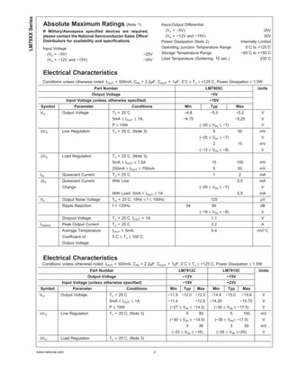


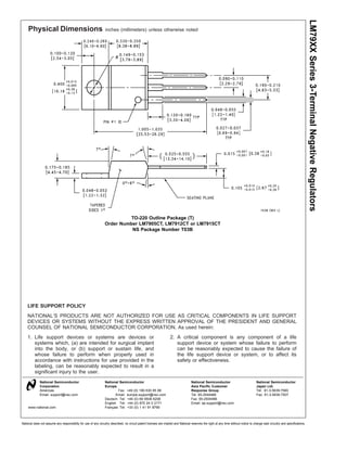


The LM79XX series are 3-terminal negative regulators that provide -5V, -12V, and -15V outputs. They require only one external component, an output compensation capacitor. The regulators have internal current limiting and thermal shutdown protection. They are packaged in a TO-220 case and can supply up to 1.5A of output current with good line and load regulation.


