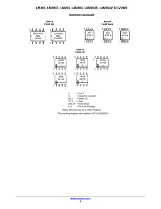
This document provides information on dual comparator integrated circuits from ON Semiconductor, including the LM393, LM393E, LM293, LM2903, LM2903E, LM2903V, and NCV2903. It includes specifications for electrical characteristics like input offset voltage, input bias current, output saturation voltage, and supply current. The document also provides application information with examples of using the comparators in zero crossing detectors, oscillators, time delay generators, and with hysteresis. Diagrams show typical comparator schematics and markings.
The LM555 is a timer integrated circuit that can generate accurate time delays or oscillations. It can operate in both monostable and astable modes using only external resistors and capacitors. The LM555 provides precision timing for applications such as timing, pulse generation, and pulse width modulation. It can source or sink up to 200mA and is available in 8-pin packages.
The LM124 series consists of four independent, high gain,
internally frequency compensated operational amplifiers
which were designed specifically to operate from a single
power supply over a wide range of voltages. Operation from
split power supplies is also possible and the low power
supply current drain is independent of the magnitude of the
power supply voltage.
Application areas include transducer amplifiers, DC gain
blocks and all the conventional op amp circuits which now
can be more easily implemented in single power supply
systems. For example, the LM124 series can be directly
operated off of the standard +5V power supply voltage which
is used in digital systems and will easily provide the required
interface electronics without requiring the additional ±15V
power supplies.
The LM231/LM331 family of integrated circuits are precision voltage-to-frequency converters suited for analog-to-digital conversion and other applications. They output a pulse train whose frequency is precisely proportional to the input voltage. The devices use a temperature-compensated bandgap reference for excellent accuracy over a wide temperature range from 4V to 40V supply. They can drive TTL loads or provide higher voltage outputs while being short-circuit proof. Key features include high linearity, temperature stability, and wide dynamic range at frequencies from 1Hz to 100kHz.
The document describes the LM741 operational amplifier. It provides general information on the device, including that it is a general purpose operational amplifier that improves upon previous standards. It offers features like overload protection and freedom from oscillations. The LM741C/E variants have their performance guaranteed over a wider temperature range than other variants. Electrical characteristics and specifications are provided in tables. Packaging and connection diagrams are displayed.
This document provides information on dual operational amplifiers including the LM358, LM258, LM2904, and LM2904V. It includes maximum ratings, electrical characteristics, representative schematics, circuit descriptions, and example applications such as voltage references, oscillators, filters, and comparators. The amplifiers feature low power, rail-to-rail input/output, and compatibility with popular operational amplifiers.
The document describes dual operational amplifiers - the LM2904, LM358/LM358A, and LM258/LM258A. These devices consist of two independent op-amps designed to operate from a single power supply over a wide voltage range of 3V to 32V. They feature high gain, frequency compensation, and can source or sink output currents up to 30mA. The document provides detailed specifications, electrical characteristics, typical performance curves, and mechanical dimensions of the 8-pin DIP package for the devices.
This document summarizes a DC voltage current source/monitor device that is suitable for testing high-voltage semiconductors and LED luminaires. The device can output voltages up to +250V and currents up to ±320mA with high accuracy of ±0.02%. It has various measurement and sweep functions including pulse measurement with a minimum pulse width of 50μs. The device also has a suspend function to control the output status and prevent transient currents when connecting voltage sources.
PBZ Series Intelligent Bi-Polar Power Supplies
The PBZ series is a bipolar type DC regulated power source that can continuously change both + and – polarities passing through 0 without changing the output terminal.
By adopting a “Switching + Linear” system, the PBZ is able to realize both drastic weight reduction as well as high speed and low noise operation. Since operation covers 4 quadrants, power can be both supplied (source) and absorbed (sink). The PBZ can also drive inductive or capacitive loads. The unit also equips a signal generator function which enables waveform and sequence creation. The PBZ is also capable of synchronized operation which is required for voltage variation tests, and it can also be expanded for large current applications through master-slave parallel operation.
ADCMT DC Voltage Current Source Monitor 6253
Best for development or evaluation of high-precision electronic components
by wide source range and 6½-digit measurement resolution
The DC voltage current source/monitor 6253 is suitable as power source for evaluation of semiconductors and other electronic components and as power source of characteristic systems. In addition to high accuracy, high stability and low noise of our strengths, the 6253 realizes higher precision features such as 5½ digit source resolution, 6½-digit measurement resolution and basis accuracy of ±0.02 %. Furthermore, the 6253 can support various applications by the sweep functions, high-speed pulse source function with a minimum pulse width of 25 μs, the variable integration function and the newly adopted variable slew rate function.
https://www.n-denkei.com/singapore/inquiry/
The LM741 series are general purpose operational amplifiers that are direct replacements for popular op amp models. They offer features like overload protection, no latch-up, and stability. The LM741C/E variants have their performance guaranteed over a 0°C to 70°C range instead of -55°C to 125°C. The document provides electrical characteristics for the LM741 models including input offset voltage, bias current, gain, output voltage and current specifications.
1. The document provides specifications for programmable AC/DC power sources models EC750SA and EC1000SA, including output voltage, current and power ranges, waveform types, frequency settings, measurement functions, interfaces, and control features.
2. Key features include stable output under various load conditions, a peak current output up to 4 times the rated current, sequence functionality for automated testing, and measurement and protection functions.
3. The units support applications in testing electronics, automobiles, appliances and more through a range of output modes, waveform types, sequencing, and integrated measurement and control capabilities.
This document describes the UC1907, UC2907, and UC3907 load share controller ICs. These ICs allow multiple independent power modules to share load current proportionately by controlling each module's power stage based on a common current share bus voltage. Key features include accurate voltage and current sensing and amplification, adjustable current sharing through independent voltage feedback loops, and designation of a master module to ensure current matching within 2.5% across modules. The IC resides on each power module to provide closed-loop voltage control based on the current share bus signal.
SS9620 PV Cell Evaluation System
Overall Evaluation System Capable of Measuring
Solar Cell Dark Current
l Dark current measurement of large solar cell modules by connecting the booster unit 46015
l Precise parallel resistance measurement and bypass diode
evaluation by using the reverse polarity unit
l Maximum output power of 300W (300V/±1A, 30V/±10A)
l High speed measurement at 100 points in 5ms
l 50μs to 6s/point that supports various kinds of solar cells
l Sampling for short-pulsed, middle-pulsed and long-pulsed light
l 3-slope linear sweep function to measure finely around Isc,
Pmax and Voc
These comparators are designed for use in level detection, low-level sensing and memory applications. They can operate from a single or split power supply and have low input bias current, offset current and offset voltage. They are compatible with TTL and CMOS logic and have ESD protection diodes on the inputs to increase reliability.
This document provides specifications for Texas Instruments' μA7800 series of positive voltage regulators. The μA7800 series includes 5 models of 3-terminal positive voltage regulators (μA7805, μA7808, μA7810, μA7812, μA7815) that can provide regulated output voltages of 5V, 8V, 10V, 12V, and 15V respectively, with an output current of up to 1.5A. The document includes details on electrical characteristics, thermal properties, ordering information and package types for each model.
The LM317 is an adjustable 3-terminal positive voltage regulator chip capable of supplying 1.5A over a voltage range of 3V to 40V. It requires only two external resistors to set the output voltage and offers better performance than fixed regulators. It provides protection against overloads, overheating, and short circuits. Common applications include programmable and precision current regulation. It can adjust output from 1.2V to 37V with input regulation of 0.01% and output regulation of 0.1%. Maximum operating temperature is 125°C.
This document summarizes the features of the KG Load Station Series 300W/1000W electronic loads. It has a revolutionary UI like an oscilloscope for easy operation. It realizes less 35% weight than previous models. It can operate just like a resistor with no minimum voltage requirement. It has high speed current control and 4 models from 300W to 1000W in 125V and 500V ranges.
The document describes the LM117/LM217/LM317 adjustable voltage regulators. Key points:
- They can supply over 1.5A of load current and adjust the output voltage from 1.2V to 37V using only a resistor divider.
- They come in TO-220, TO-220FP, TO-3, and D2PAK packages and have protection for overcurrent, overtemperature, and output short circuits.
- The output voltage is set using an internal 1.25V reference and an external resistor divider according to the equation VO = VREF (1 + R2/R1) + IADJR2. Capacitors can be added for
This document provides information about the LM117, LM317A, and LM317 3-terminal adjustable voltage regulators. It describes their capabilities of supplying over 1.5A over an output range of 1.2V to 37V. They require only two external resistors to set the output voltage and offer better than standard regulation. The regulators provide full overload protection including current limiting and are available in standard transistor packages.
Voltage to-frequency and frequency-to-voltage converterThe Hoa Nguyen
The document describes a voltage-to-frequency converter (VFC32) that provides an output frequency accurately proportional to its input voltage. It has excellent linearity of ±0.01% at 10kHz and ±0.05% at 100kHz. It can operate up to 500kHz and can be configured as either a voltage-to-frequency converter or frequency-to-voltage converter. It is available in plastic DIP, surface mount, and metal packages with commercial, industrial, and military temperature ranges.
The document describes the UCC3895 BiCMOS advanced phase-shift PWM controller. It has features such as programmable output turn-on delay, adaptive delay set, bidirectional oscillator synchronization, and voltage-mode or current-mode control. It can operate at frequencies up to 1 MHz with typical operating current of 5 mA at 500 kHz. The UCC3895 is a phase-shift PWM controller that implements full-bridge power stage control by phase shifting one half-bridge with respect to the other, allowing constant frequency pulse-width modulation with zero-voltage switching for high efficiency at high frequencies. It improves on previous controller families with additional features such as enhanced control logic and adaptive delay set.
This document provides information about the TLV3491, TLV3492, and TLV3494 push-pull output comparators. Key details include:
- They feature a fast 6μs response time and low power capability of <1.2μA operating from 1.8V to 5.5V.
- Input common-mode range extends beyond the supply rails, making them suitable for low-voltage applications.
- They are available in small packages like SOT23 and SOIC suitable for portable and space-constrained applications.
- Applications include portable medical equipment, wireless security systems, remote controls, and other low power systems.
Omicron CMC 256plus High Precision Relay Test Set and Universal Calibrator Da...Angus Sankaran
Protection test set and universal calibrator in one device
Testing of all relay generations - electromechanical, static, numerical, IEC 61850
Integrated network for testing IEC 61850 IEDs
This document provides information about the LM150/LM350A/LM350 series of adjustable 3-terminal positive voltage regulators, including:
- They can supply over 3A over an output range of 1.2V to 33V and only require 2 external resistors to set the output voltage.
- They provide full overload protection including current limit, thermal overload protection and safe area protection.
- No external capacitors are typically needed unless the regulator is more than 6 inches from the input filter capacitors.
The document describes the LM78XX series of 3-terminal positive voltage regulators. Key details include:
- The regulators come in a TO-220 package and provide fixed output voltages of 5, 6, 8, 9, 10, 12, 15, 18, 24V.
- They can supply up to 1A of output current with features like overload protection, short-circuit protection, and safe operating area protection.
- Electrical characteristics are provided for various models, showing parameters like line/load regulation, noise, temperature drift, and maximum ratings.
This document provides data sheets for several quad operational amplifier integrated circuits, including the CA124, CA224, CA324, LM324, and LM2902. It summarizes their key specifications such as operating temperature range, voltage gain, bandwidth, input/output voltage ranges, power requirements, and packaging options. The amplifiers each contain four independent high-gain op-amps on a single chip and are designed for use in commercial, industrial and military applications requiring operation from single or dual power supplies.
This document provides technical specifications for an ABB REF615 ANSI feeder protection relay. It includes 30 tables that specify details such as power supply requirements, input/output ratings, communication protocols, environmental testing procedures, EMC compliance, and supported protection functions. The relay is approved to relevant safety and EMC standards and directives.
The LM3915 is an integrated circuit that drives 10 LEDs or other displays in a logarithmic bar graph fashion based on an input analog voltage. It contains an adjustable voltage reference, precision voltage divider, and 10 comparators to light the correct number of LEDs corresponding to the input voltage level. The full-scale input range and LED current can be programmed. It can operate from a single 3V to 25V supply and is suitable for applications like audio level meters, power meters, and signal strength indicators.
The LM3914 is an integrated circuit that senses analog voltage levels and drives 10 LEDs to provide a linear analog display. It contains an adjustable voltage reference and accurate 10-step voltage divider to compare input voltages. The outputs are individually current regulated and can drive LEDs, LCDs, or vacuum fluorescent displays in either a moving dot or bar graph display mode. The simple circuit requires few external components and can operate over a wide supply voltage range from less than 3V.
The LM555 is a highly stable integrated circuit used for generating precise time delays or oscillation. It can operate in both monostable (one-shot) and astable (oscillator) modes using only external resistors and capacitors. In monostable mode, the output is triggered on for a precise time determined by a single resistor and capacitor. In astable mode, the output oscillates at a frequency and duty cycle set by two resistors and one capacitor. The LM555 has applications in precision timing, pulse generation, and frequency modulation.
The LM555 is an integrated circuit used for generating accurate time delays or oscillations. It can be used in monostable or astable configuration. In monostable mode, the time delay is controlled by one resistor and capacitor. In astable mode, the frequency and duty cycle are controlled by two resistors and one capacitor. The circuit can be triggered and reset. The output can source or sink up to 200mA. It has applications in precision timing, pulse generation, and sequential timing.
This document provides information about the LM3722/LM3723/LM3724 microprocessor reset circuits. These circuits monitor the power supply voltages in microprocessor systems and provide a reset signal to the microprocessor during power up, power down, brownout conditions, and when a manual reset button is pressed. The reset signal remains active for at least 100ms after the power supply voltage rises above the reset threshold. The LM3722 has an active-low reset output, the LM3723 has an active-high reset output, and the LM3724 has an active-low open-drain reset output. These circuits are available with reset thresholds of 2.5V, 3.3V and 5V and have a
This document provides information about the LM3722/LM3723/LM3724 microprocessor reset circuits. These circuits monitor the power supply voltages in microprocessor systems and provide a reset signal to the microprocessor during power up, power down, brownout conditions, and via a manual reset. The LM3722 has an active-low reset output, the LM3723 has an active-high reset output, and the LM3724 has an active-low open-drain reset output. They are available with reset thresholds of 4.63V, 3.08V, and 2.32V to monitor 5V, 3.3V, and 2.5V supplies respectively. The reset output remains active for at
The LM79XX series are 3-terminal negative regulators that provide -5V, -12V, and -15V outputs. They require only one external component, an output compensation capacitor. The regulators have internal current limiting and thermal shutdown protection. They are packaged in a TO-220 case and can supply up to 1.5A of output current with good line and load regulation.
The AD598 is a monolithic linear variable differential transformer (LVDT) signal conditioning subsystem that converts mechanical position to a scaled DC voltage output with high accuracy. It contains an internal oscillator, amplifier, and filter to drive the LVDT primary and convert the LVDT secondary output into a unipolar or bipolar DC voltage. Key benefits include excellent temperature stability, insensitivity to phase shifts or null voltages, and no required adjustments. It is available in different temperature ranges and packages.
This document provides specifications for the MAX232 dual driver/receiver IC, which includes a capacitive voltage generator to supply standard TIA/EIA-232 voltage levels from a single 5V supply. It operates up to 120kbps and has ESD protection exceeding 15kV. The MAX232 contains two drivers, two receivers, and a charge pump to convert voltages for serial communication interfaces.
The TPS65023 is an integrated power management IC that provides three highly efficient step-down converters and two low-dropout regulators. It is designed to power applications running from a single lithium-ion battery cell, such as digital media players and digital cameras. The IC includes a 1.5A step-down converter for the processor core, a 1.2A converter for system voltage, and a 1A converter for memory voltage. It also has a 30mA low-dropout regulator for real-time clock functions and two 200mA general-purpose low-dropout regulators. All components are selectable and configurable through the IC's serial interface.
The document provides specifications for the UC2842/3/4/5 and UC3842/3/4/5 family of current mode PWM controller ICs. The controllers are optimized for offline and DC-DC converters with features such as low start-up current, automatic feed forward compensation, current limiting, and undervoltage lockout. Key specifications include a switching frequency up to 500kHz, current sense gain of 2.8-3.2V/V, and maximum duty cycles from 0-100% depending on the specific model. Application diagrams show examples of using the ICs in offline flyback converter and DC-DC converter designs.
The SN75176A is a bidirectional transceiver that operates from a single 5V supply. It combines a 3-state differential line driver and differential line receiver. The driver can handle loads up to 60mA and features current limiting and thermal shutdown protection. The receiver has a minimum input impedance of 12kΩ and input sensitivity of ±200mV. It is designed for use on multipoint bus lines in noisy environments.
The TL082 is a dual JFET-input operational amplifier that provides high speed and low noise performance. It has an internally trimmed input offset voltage, low input bias current, wide gain bandwidth of 4 MHz, and high slew rate of 13 V/μs. The TL082 can be used in applications such as high speed integrators, sample and hold circuits, and other circuits requiring fast operation and low noise.
The document summarizes the features and specifications of the SPX29300/01/02/03 3A low dropout voltage regulators. Key points:
- They are 3A voltage regulators with a low dropout voltage of 450mV at 3A output current, designed for low voltage applications requiring fast response times.
- Features include adjustable and fixed output options, reverse battery and overcurrent protection, tight load and line regulation, and fast transient response.
- Electrical specifications include 1% output accuracy, low quiescent current, and temperature coefficients.
- Applications include powering computer components, high efficiency power supplies, and battery chargers.
- Typical circuits shown regulate the output voltage via feedback resistors
The NCP3170 is a synchronous PWM switching converter that operates from 4.5V to 18V and sources up to 3A of output current. It is capable of producing output voltages as low as 0.8V and incorporates current mode control with many features like soft start, power good detection, and fixed switching frequencies set internally to reduce external components. It is available in an 8-pin SOIC package and is suitable for applications such as set top boxes, DVD/Blu-ray drives, LCD monitors/TVs, and telecom equipment.
The MAX6603 is a dual-channel signal conditioner that amplifies signals from two external platinum RTD temperature sensors and provides the temperature information as two independent analog output voltages. It excites the RTDs with a constant current, amplifies the signal, and provides a ratiometric output voltage that is compatible with microcontroller ADCs. The device monitors the RTDs for faults and will assert diagnostic outputs low if a fault is detected on either input. It is available in a small 10-pin package and operates over an automotive temperature range from a single power supply.
This document provides specifications for the μA723 precision voltage regulator integrated circuit, including:
- Electrical characteristics such as input/output voltage ranges, current limits, and temperature stability.
- Application information such as resistor values needed for standard output voltages and formulas for calculating intermediate voltages.
- A functional block diagram and schematic showing the internal components and typical external connections.
- Packaging and temperature rating options for the chip in plastic DIP and small outline packages.
This document provides information on the MJE13003 NPN silicon transistor from Unisonic Technologies Co., Ltd. It describes the transistor as being designed for high-voltage, high-speed power switching in inductive circuits. Key features include a reverse biased safe operating area with inductive loads up to 1.5 amps and a typical fall time of 290ns at 1 amp and 100°C. The transistor has applications in switching regulators, inverters, motor controls, solenoid drivers, and deflection circuits. Electrical characteristics and maximum ratings are provided in tables and graphs.
The document describes the LM124 series of low power quad operational amplifiers. It provides specifications for the amplifiers including their ability to operate from a single power supply over a wide voltage range, low current drain, high gain, wide bandwidth, and temperature stability. Application areas are listed as transducer amplifiers, DC gain blocks, and conventional op amp circuits that can now be implemented in single power supply systems.
The MAX1830/MAX1831 are 3A, 1MHz step-down DC-DC converters with synchronous rectification and internal switches. They provide high efficiency conversion from 5V and 3.3V inputs to adjustable low-voltage outputs between 1.1V to the input voltage. The devices integrate a PMOS power switch and NMOS synchronous rectifier to deliver up to 3A continuous current with no external diode required. They offer efficiencies as high as 94% and operate over an input voltage range of 3V to 5.5V.
Expanding Access to Affordable At-Home EV Charging by Vanessa WarheitForth
Vanessa Warheit, Co-Founder of EV Charging for All, gave this presentation at the Forth Addressing The Challenges of Charging at Multi-Family Housing webinar on June 11, 2024.
What Could Be Behind Your Mercedes Sprinter's Power Loss on Uphill RoadsSprinter Gurus
Unlock the secrets behind your Mercedes Sprinter's uphill power loss with our comprehensive presentation. From fuel filter blockages to turbocharger troubles, we uncover the culprits and empower you to reclaim your vehicle's peak performance. Conquer every ascent with confidence and ensure a thrilling journey every time.
Understanding Catalytic Converter Theft:
What is a Catalytic Converter?: Learn about the function of catalytic converters in vehicles and why they are targeted by thieves.
Why are They Stolen?: Discover the valuable metals inside catalytic converters (such as platinum, palladium, and rhodium) that make them attractive to criminals.
Steps to Prevent Catalytic Converter Theft:
Parking Strategies: Tips on where and how to park your vehicle to reduce the risk of theft, such as parking in well-lit areas or secure garages.
Protective Devices: Overview of various anti-theft devices available, including catalytic converter locks, shields, and alarms.
Etching and Marking: The benefits of etching your vehicle’s VIN on the catalytic converter or using a catalytic converter marking kit to make it traceable and less appealing to thieves.
Surveillance and Monitoring: Recommendations for using security cameras and motion-sensor lights to deter thieves.
Statistics and Insights:
Theft Rates by Borough: Analysis of data to determine which borough in NYC experiences the highest rate of catalytic converter thefts.
Recent Trends: Current trends and patterns in catalytic converter thefts to help you stay aware of emerging hotspots and tactics used by thieves.
Benefits of This Presentation:
Awareness: Increase your awareness about catalytic converter theft and its impact on vehicle owners.
Practical Tips: Gain actionable insights and tips to effectively prevent catalytic converter theft.
Local Insights: Understand the specific risks in different NYC boroughs, helping you take targeted preventive measures.
This presentation aims to equip you with the knowledge and tools needed to protect your vehicle from catalytic converter theft, ensuring you are prepared and proactive in safeguarding your property.
Implementing ELDs or Electronic Logging Devices is slowly but surely becoming the norm in fleet management. Why? Well, integrating ELDs and associated connected vehicle solutions like fleet tracking devices lets businesses and their in-house fleet managers reap several benefits. Check out the post below to learn more.
Ever been troubled by the blinking sign and didn’t know what to do?
Here’s a handy guide to dashboard symbols so that you’ll never be confused again!
Save them for later and save the trouble!
Welcome to ASP Cranes, your trusted partner for crane solutions in Raipur, Chhattisgarh! With years of experience and a commitment to excellence, we offer a comprehensive range of crane services tailored to meet your lifting and material handling needs.
At ASP Cranes, we understand the importance of reliable and efficient crane operations in various industries, from construction and manufacturing to logistics and infrastructure development. That's why we strive to deliver top-notch solutions that enhance productivity, safety, and cost-effectiveness for our clients.
Our services include:
Crane Rental: Whether you need a crawler crane for heavy lifting or a hydraulic crane for versatile operations, we have a diverse fleet of well-maintained cranes available for rent. Our rental options are flexible and can be customized to suit your project requirements.
Crane Sales: Looking to invest in a crane for your business? We offer a wide selection of new and used cranes from leading manufacturers, ensuring you find the perfect equipment to match your needs and budget.
Crane Maintenance and Repair: To ensure optimal performance and safety, regular maintenance and timely repairs are essential for cranes. Our team of skilled technicians provides comprehensive maintenance and repair services to keep your equipment running smoothly and minimize downtime.
Crane Operator Training: Proper training is crucial for safe and efficient crane operation. We offer specialized training programs conducted by certified instructors to equip operators with the skills and knowledge they need to handle cranes effectively.
Custom Solutions: We understand that every project is unique, which is why we offer custom crane solutions tailored to your specific requirements. Whether you need modifications, attachments, or specialized equipment, we can design and implement solutions that meet your needs.
At ASP Cranes, customer satisfaction is our top priority. We are dedicated to delivering reliable, cost-effective, and innovative crane solutions that exceed expectations. Contact us today to learn more about our services and how we can support your project in Raipur, Chhattisgarh, and beyond. Let ASP Cranes be your trusted partner for all your crane needs!
EV Charging at MFH Properties by Whitaker JamiesonForth
Whitaker Jamieson, Senior Specialist at Forth, gave this presentation at the Forth Addressing The Challenges of Charging at Multi-Family Housing webinar on June 11, 2024.
2. LM393, LM393E, LM293, LM2903, LM2903E, LM2903V, NCV2903
www.onsemi.com
2
MAXIMUM RATINGS
Rating Symbol Value Unit
Power Supply Voltage VCC +36 or ±18 V
Input Differential Voltage VIDR 36 V
Input Common Mode Voltage Range (Note 1) VICR −0.3 to +36 V
Output Voltage VO 36 V
Output Short Circuit−to−Ground
Output Sink Current (Note 2)
ISC
ISink
Continuous
20
mA
Power Dissipation @ TA = 25°C
Derate above 25°C
PD
1/RqJA
570
5.7
mW
mW/°C
Operating Ambient Temperature Range
LM293
LM393, LM393E
LM2903, LM2903E
LM2903V, NCV2903 (Note 3)
TA
−25 to +85
0 to +70
−40 to +105
−40 to +125
°C
Maximum Operating Junction Temperature
LM393, LM393E, LM2903, LM2903E, LM2903V
LM293, NCV2903
TJ(max)
150
150
°C
Storage Temperature Range Tstg −65 to +150 °C
Stresses exceeding those listed in the Maximum Ratings table may damage the device. If any of these limits are exceeded, device functionality
should not be assumed, damage may occur and reliability may be affected.
1. For supply voltages less than 36 V, the absolute maximum input voltage is equal to the supply voltage.
2. The maximum output current may be as high as 20 mA, independent of the magnitude of VCC, output short circuits to VCC can cause
excessive heating and eventual destruction.
3. NCV2903 is qualified for automotive use.
ESD RATINGS
Rating HBM MM Unit
ESD Protection at any Pin (Human Body Model − HBM, Machine Model − MM)
NCV2903 (Note 3)
LM393E, LM2903E
LM393DG/DR2G, LM2903DG/DR2G
All Other Devices
2000
1500
250
1500
200
150
100
150
V
V
V
V
3. LM393, LM393E, LM293, LM2903, LM2903E, LM2903V, NCV2903
www.onsemi.com
3
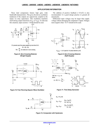
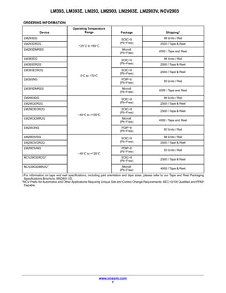
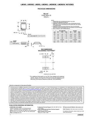
ELECTRICAL CHARACTERISTICS (VCC = 5.0 Vdc, Tlow ≤ TA ≤ Thigh, unless otherwise noted.)
Characteristic Symbol
LM293, LM393, LM393E
LM2903/E/V,
NCV2903
UnitMin Typ Max Min Typ Max
Input Offset Voltage (Note 5) VIO mV
TA = 25°C − ±1.0 ±5.0 − ±2.0 ±7.0
Tlow ≤ TA ≤ Thigh − − ±9.0 − ±9.0 ±15
Input Offset Current IIO nA
TA = 25°C − ±5.0 ±50 − ±5.0 ±50
Tlow ≤ TA ≤ Thigh − − ±150 − ±50 ±200
Input Bias Current (Note 6) IIB nA
TA = 25°C − 20 250 − 20 250
Tlow ≤ TA ≤ Thigh − − 400 − 20 500
Input Common Mode Voltage Range (Note 6) VICR V
TA = 25°C 0 − VCC −1.5 0 − VCC −1.5
Tlow ≤ TA ≤ Thigh 0 − VCC −2.0 0 − VCC −2.0
Voltage Gain AVOL 50 200 − 25 200 − V/mV
RL ≥ 15 kW, VCC = 15 Vdc, TA = 25°C
Large Signal Response Time − − 300 − − 300 − ns
Vin = TTL Logic Swing, Vref = 1.4 Vdc
VRL = 5.0 Vdc, RL = 5.1 kW, TA = 25°C
Response Time (Note 8) tTLH − 1.3 − − 1.5 − ms
VRL = 5.0 Vdc, RL = 5.1 kW, TA = 25°C
Input Differential Voltage (Note 9) VID − − VCC − − VCC V
All Vin ≥ GND or V− Supply (if used)
Output Sink Current ISink 6.0 16 − 6.0 16 − mA
Vin ≥ 1.0 Vdc, Vin+ = 0 Vdc, VO ≤ 1.5 Vdc TA = 25°C
Output Saturation Voltage VOL mV
Vin ≥ 1.0 Vdc, Vin+ = 0, ISink ≤ 4.0 mA, TA = 25°C − 150 400 − − 400
Tlow ≤ TA ≤ Thigh − − 700 − 200 700
Output Leakage Current IOL nA
Vin− = 0 V, Vin+ ≥ 1.0 Vdc, VO = 5.0 Vdc, TA = 25°C − 0.1 − − 0.1 −
Vin− = 0 V, Vin+ ≥ 1.0 Vdc, VO = 30 Vdc,
Tlow ≤ TA ≤ Thigh − − 1000 − − 1000
Supply Current ICC mA
RL = ∞ Both Comparators, TA = 25°C − 0.4 1.0 − 0.4 1.0
RL = ∞ Both Comparators, VCC = 30 V − − 2.5 − − 2.5
Product parametric performance is indicated in the Electrical Characteristics for the listed test conditions, unless otherwise noted. Product
performance may not be indicated by the Electrical Characteristics if operated under different conditions.
LM293 Tlow = −25°C, Thigh = +85°C
LM393, LM393E Tlow = 0°C, Thigh = +70°C
LM2903, LM2903E Tlow = −40°C, Thigh = +105°C
LM2903V & NCV2903 Tlow = −40°C, Thigh = +125°C
NCV2903 is qualified for automotive use.
4. The maximum output current may be as high as 20 mA, independent of the magnitude of VCC, output short circuits to VCC can cause
excessive heating and eventual destruction.
5. At output switch point, VO]1.4 Vdc, RS = 0 W with VCC from 5.0 Vdc to 30 Vdc, and over the full input common mode range
(0 V to VCC = −1.5 V).
6. Due to the PNP transistor inputs, bias current will flow out of the inputs. This current is essentially constant, independent of the output state,
therefore, no loading changes will exist on the input lines.
7. Input common mode of either input should not be permitted to go more than 0.3 V negative of ground or minus supply. The upper limit of
common mode range is VCC −1.5 V.
8. Response time is specified with a 100 mV step and 5.0 mV of overdrive. With larger magnitudes of overdrive faster response times are
obtainable.
9. The comparator will exhibit proper output state if one of the inputs becomes greater than VCC, the other input must remain within the common
mode range. The low input state must not be less than −0.3 V of ground or minus supply.
4. LM393, LM393E, LM293, LM2903, LM2903E, LM2903V, NCV2903
www.onsemi.com
4
LM293/393 LM2903
Figure 2. Input Bias Current versus
Power Supply Voltage
Figure 3. Input Bias Current versus
Power Supply Voltage
Figure 4. Output Saturation Voltage
versus Output Sink Current
Figure 5. Output Saturation Voltage
versus Output Sink Current
Figure 6. Power Supply Current versus
Power Supply Voltage
Figure 7. Power Supply Current versus
Power Supply Voltage
VCC, SUPPLY VOLTAGE (Vdc) VCC, SUPPLY VOLTAGE (Vdc)
ISink, OUTPUT SINK CURRENT (mA) ISink, OUTPUT SINK CURRENT (mA)
I,INPUTBIASCURRENT(nA)IBV,SATURATIONVOLTAGE(Vdc)OLI,SUPPLYCURRENT(mA)CC
7
0 5 10 15 20 25 30 35 40
13
0 5 10 15 20 25 30 35 40
10
1.0
0.1
0.01
0.001
0.01 0.1 1.0 10 100
1.0
0.8
0.6
0.4
0.2
0
5.0 10 15 20 25 30 35 40
1.2
0.4
10
1.0
0.1
0.01
0.001
0.01 0.1 1.0 10 100
0 5.0 10 15 20 25 30 35 40
TA = 0°C
TA = +25°C
TA = +70° C
TA = +125°C
RL = R
TA = 0° C
TA = +25° C
TA = +25° C
TA = 0° C
TA = +25° C
TA = -40° C
TA = -40° C
TA = 0° C
TA = +25° C
TA = +85° C
1.0
0.8
0.6
I,SUPPLYCURRENT(mA)CCV,SATURATIONVOLTAGE(Vdc)OLI,INPUTBIASCURRENT(nA)IB
TA = +125°C
RL = R
TA = -40°C
TA = +70°C
TA = +125°C
TA = -55° C
Out of
Saturation
TA = +85° C
Out of
Saturation
TA = -55° C
8
9
10
11
12
13
14
TA = +85°C
TA = +105°C
15
17
19
21
23
25
TA = 0°C
TA = +25°C
TA = -40°C
TA = +70°C
TA = +125°C
TA = +85°C
TA = +105°C
5. LM393, LM393E, LM293, LM2903, LM2903E, LM2903V, NCV2903
www.onsemi.com
5
APPLICATIONS INFORMATION
These dual comparators feature high gain, wide
bandwidth characteristics. This gives the device oscillation
tendencies if the outputs are capacitively coupled to the
inputs via stray capacitance. This oscillation manifests
itself during output transitions (VOL to VOH). To alleviate
this situation, input resistors <10 kW should be used.
The addition of positive feedback (<10 mV) is also
recommended. It is good design practice to ground all
unused pins.
Differential input voltages may be larger than supply
voltage without damaging the comparator’s inputs. Voltages
more negative than −0.3 V should not be used.
Figure 8. Zero Crossing Detector
(Single Supply)
Figure 9. Zero Crossing Detector
(Split Supply)
Figure 10. Free−Running Square−Wave Oscillator Figure 11. Time Delay Generator
Figure 12. Comparator with Hysteresis
10
D1 prevents input from going negative by more than 0.6 V.
R1 + R2 = R3
R3 ≤
R5
for small error in zero crossing.
Vin
10 k
D1
R1
8.2 k
6.8 k
R2
15 k
R3
+15 V
10 m
R5
220 k
R4
220 k
LM393
Vin(min) [ 0.4 V peak for 1% phase distortion (DQ).
*
Q
+VCC
10 k
Vin
-VEE
Vin
Vin(min)
VCC
VO
- VEE
DQ
Q
LM393
-
+
LM393
51 k
51 k
51 k
RL
10 k
VCC
VCC
VCC
VO
VO
t
0
1.0 mW
0.001 mF
-
+
LM393
VCC VCC
VO
Vin
VO
+ Vref
Vref
Vref
0
0
0
VC
tO
t
``ON'' for t tO + Dt
where:
Dt = RC ȏ n (
Vref
VCC
)
R RL
VC C
LM393
-
+
RS
VCC
RL
Vref
R1
R2
RS = R1 | | R2
Vth1 = Vref +
(VCC -Vref) R1
R1 + R2 + RL
Vth2 = Vref -
(Vref -VO Low) R1
R1 + R2
R1
tȏ
+
-
LM393
)
*
)
6. LM393, LM393E, LM293, LM2903, LM2903E, LM2903V, NCV2903
www.onsemi.com
6
MARKING DIAGRAMS
1
8
x = 2 or 3
A = Assembly Location
WL, L = Wafer Lot
YY, Y = Year
WW, W = Work Week
G, G = Pb−Free Package
PDIP−8
CASE 626
SOIC−8
CASE 751
*
*This marking diagram also applies to NCV2903DR2G
Micro8
CASE 846A
LMx93
ALYW
G
1
8
2903V
ALYW
G
1
8
2903
ALYW
G
1
8
LM393NG
AWL
YYWW
1
8
LM2903N
AWL
YYWWG
x93
AYW G
G
1
8
(Note: Microdot may be in either location)
2903
AYW G
G
1
8
903V
AYW G
G
1
8
393E
ALYW
G
1
8
2903E
ALYW
G
1
8
7. LM393, LM393E, LM293, LM2903, LM2903E, LM2903V, NCV2903
www.onsemi.com
7
ORDERING INFORMATION
Device
Operating Temperature
Range Package Shipping†
LM293DG
−25°C to +85°C
SOIC−8
(Pb−Free)
98 Units / Rail
LM293DR2G 2500 / Tape & Reel
LM293DMR2G Micro8
(Pb−Free)
4000 / Tape and Reel
LM393DG
0°C to +70°C
SOIC−8
(Pb−Free)
98 Units / Rail
LM393DR2G 2500 / Tape & Reel
LM393EDR2G SOIC−8
(Pb−Free)
2500 / Tape & Reel
LM393NG PDIP−8
(Pb−Free)
50 Units / Rail
LM393DMR2G Micro8
(Pb−Free)
4000 / Tape and Reel
LM2903DG
−40°C to +105°C
SOIC−8
(Pb−Free)
98 Units / Rail
LM2903DR2G 2500 / Tape & Reel
LM2903EDR2G SOIC−8
(Pb−Free)
2500 / Tape & Reel
LM2903DMR2G Micro8
(Pb−Free)
4000 / Tape and Reel
LM2903NG PDIP−8
(Pb−Free)
50 Units / Rail
LM2903VDG
−40°C to +125°C
SOIC−8
(Pb−Free)
98 Units / Rail
LM2903VDR2G 2500 / Tape & Reel
LM2903VNG PDIP−8
(Pb−Free)
50 Units / Rail
NCV2903DR2G* SOIC−8
(Pb−Free)
2500 / Tape & Reel
NCV2903DMR2G* Micro8
(Pb−Free)
4000 / Tape & Reel
†For information on tape and reel specifications, including part orientation and tape sizes, please refer to our Tape and Reel Packaging
Specifications Brochure, BRD8011/D.
*NCV Prefix for Automotive and Other Applications Requiring Unique Site and Control Change Requirements; AEC−Q100 Qualified and PPAP
Capable.
8. LM393, LM393E, LM293, LM2903, LM2903E, LM2903V, NCV2903
www.onsemi.com
8
PACKAGE DIMENSIONS
PDIP−8
N, AN, VN SUFFIX
CASE 626−05
ISSUE P
1 4
58
b2
NOTE 8
D
b
L
A1
A
eB
E
A
TOP VIEW
C
SEATING
PLANE
0.010 C A
SIDE VIEW
END VIEW
END VIEW
WITH LEADS CONSTRAINED
DIM MIN MAX
INCHES
A −−−− 0.210
A1 0.015 −−−−
b 0.014 0.022
C 0.008 0.014
D 0.355 0.400
D1 0.005 −−−−
e 0.100 BSC
E 0.300 0.325
M −−−− 10
−−− 5.33
0.38 −−−
0.35 0.56
0.20 0.36
9.02 10.16
0.13 −−−
2.54 BSC
7.62 8.26
−−− 10
MIN MAX
MILLIMETERS
NOTES:
1. DIMENSIONING AND TOLERANCING PER ASME Y14.5M, 1994.
2. CONTROLLING DIMENSION: INCHES.
3. DIMENSIONS A, A1 AND L ARE MEASURED WITH THE PACK-
AGE SEATED IN JEDEC SEATING PLANE GAUGE GS−3.
4. DIMENSIONS D, D1 AND E1 DO NOT INCLUDE MOLD FLASH
OR PROTRUSIONS. MOLD FLASH OR PROTRUSIONS ARE
NOT TO EXCEED 0.10 INCH.
5. DIMENSION E IS MEASURED AT A POINT 0.015 BELOW DATUM
PLANE H WITH THE LEADS CONSTRAINED PERPENDICULAR
TO DATUM C.
6. DIMENSION eB IS MEASURED AT THE LEAD TIPS WITH THE
LEADS UNCONSTRAINED.
7. DATUM PLANE H IS COINCIDENT WITH THE BOTTOM OF THE
LEADS, WHERE THE LEADS EXIT THE BODY.
8. PACKAGE CONTOUR IS OPTIONAL (ROUNDED OR SQUARE
CORNERS).
E1 0.240 0.280 6.10 7.11
b2
eB −−−− 0.430 −−− 10.92
0.060 TYP 1.52 TYP
E1
M
8X
c
D1
B
A2 0.115 0.195 2.92 4.95
L 0.115 0.150 2.92 3.81
°°
H
NOTE 5
e
e/2
A2
NOTE 3
M B M NOTE 6
M
9. LM393, LM393E, LM293, LM2903, LM2903E, LM2903V, NCV2903
www.onsemi.com
9
PACKAGE DIMENSIONS
SOIC−8 NB
CASE 751−07
ISSUE AK
SEATING
PLANE
1
4
58
N
J
X 45_
K
NOTES:
1. DIMENSIONING AND TOLERANCING PER
ANSI Y14.5M, 1982.
2. CONTROLLING DIMENSION: MILLIMETER.
3. DIMENSION A AND B DO NOT INCLUDE
MOLD PROTRUSION.
4. MAXIMUM MOLD PROTRUSION 0.15 (0.006)
PER SIDE.
5. DIMENSION D DOES NOT INCLUDE DAMBAR
PROTRUSION. ALLOWABLE DAMBAR
PROTRUSION SHALL BE 0.127 (0.005) TOTAL
IN EXCESS OF THE D DIMENSION AT
MAXIMUM MATERIAL CONDITION.
6. 751−01 THRU 751−06 ARE OBSOLETE. NEW
STANDARD IS 751−07.
A
B S
DH
C
0.10 (0.004)
DIM
A
MIN MAX MIN MAX
INCHES
4.80 5.00 0.189 0.197
MILLIMETERS
B 3.80 4.00 0.150 0.157
C 1.35 1.75 0.053 0.069
D 0.33 0.51 0.013 0.020
G 1.27 BSC 0.050 BSC
H 0.10 0.25 0.004 0.010
J 0.19 0.25 0.007 0.010
K 0.40 1.27 0.016 0.050
M 0 8 0 8
N 0.25 0.50 0.010 0.020
S 5.80 6.20 0.228 0.244
−X−
−Y−
G
MYM0.25 (0.010)
−Z−
YM0.25 (0.010) Z S X S
M
_ _ _ _
1.52
0.060
7.0
0.275
0.6
0.024
1.270
0.050
4.0
0.155
ǒ mm
inches
ǓSCALE 6:1
*For additional information on our Pb−Free strategy and soldering
details, please download the ON Semiconductor Soldering and
Mounting Techniques Reference Manual, SOLDERRM/D.
SOLDERING FOOTPRINT*
10. LM393, LM393E, LM293, LM2903, LM2903E, LM2903V, NCV2903
www.onsemi.com
10
PACKAGE DIMENSIONS
Micro8t
CASE 846A−02
ISSUE J
SBM0.08 (0.003) A ST
NOTES:
1. DIMENSIONING AND TOLERANCING PER ANSI Y14.5M, 1982.
2. CONTROLLING DIMENSION: MILLIMETER.
3. DIMENSION A DOES NOT INCLUDE MOLD FLASH, PROTRUSIONS OR GATE
BURRS. MOLD FLASH, PROTRUSIONS OR GATE BURRS SHALL NOT EXCEED
0.15 (0.006) PER SIDE.
4. DIMENSION B DOES NOT INCLUDE INTERLEAD FLASH OR PROTRUSION.
INTERLEAD FLASH OR PROTRUSION SHALL NOT EXCEED 0.25 (0.010) PER SIDE.
5. 846A-01 OBSOLETE, NEW STANDARD 846A-02.
b
ePIN 1 ID
8 PL
0.038 (0.0015)
−T−
SEATING
PLANE
A
A1 c L
DIM
A
MIN NOM MAX MIN
MILLIMETERS
−− −− 1.10 −−
INCHES
A1 0.05 0.08 0.15 0.002
b 0.25 0.33 0.40 0.010
c 0.13 0.18 0.23 0.005
D 2.90 3.00 3.10 0.114
E 2.90 3.00 3.10 0.114
e 0.65 BSC
L 0.40 0.55 0.70 0.016
−− 0.043
0.003 0.006
0.013 0.016
0.007 0.009
0.118 0.122
0.118 0.122
0.026 BSC
0.021 0.028
NOM MAX
4.75 4.90 5.05 0.187 0.193 0.199HE
HE
DD
E
*For additional information on our Pb−Free strategy and soldering
details, please download the ON Semiconductor Soldering and
Mounting Techniques Reference Manual, SOLDERRM/D.
SOLDERING FOOTPRINT*
8X 0.48
0.65
PITCH
5.25
8X
0.80
DIMENSION: MILLIMETERS
RECOMMENDED
PUBLICATION ORDERING INFORMATION
N. American Technical Support: 800−282−9855 Toll Free
USA/Canada
Europe, Middle East and Africa Technical Support:
Phone: 421 33 790 2910
Japan Customer Focus Center
Phone: 81−3−5817−1050
LM393/D
Micro8 is a trademark of International Rectifier.
LITERATURE FULFILLMENT:
Literature Distribution Center for ON Semiconductor
19521 E. 32nd Pkwy, Aurora, Colorado 80011 USA
Phone: 303−675−2175 or 800−344−3860 Toll Free USA/Canada
Fax: 303−675−2176 or 800−344−3867 Toll Free USA/Canada
Email: orderlit@onsemi.com
ON Semiconductor Website: www.onsemi.com
Order Literature: http://www.onsemi.com/orderlit
For additional information, please contact your local
Sales Representative
ON Semiconductor and are trademarks of Semiconductor Components Industries, LLC dba ON Semiconductor or its subsidiaries in the United States and/or other countries.
ON Semiconductor owns the rights to a number of patents, trademarks, copyrights, trade secrets, and other intellectual property. A listing of ON Semiconductor’s product/patent
coverage may be accessed at www.onsemi.com/site/pdf/Patent−Marking.pdf. ON Semiconductor reserves the right to make changes without further notice to any products herein.
ON Semiconductor makes no warranty, representation or guarantee regarding the suitability of its products for any particular purpose, nor does ON Semiconductor assume any liability
arising out of the application or use of any product or circuit, and specifically disclaims any and all liability, including without limitation special, consequential or incidental damages.
Buyer is responsible for its products and applications using ON Semiconductor products, including compliance with all laws, regulations and safety requirements or standards,
regardless of any support or applications information provided by ON Semiconductor. “Typical” parameters which may be provided in ON Semiconductor data sheets and/or
specifications can and do vary in different applications and actual performance may vary over time. All operating parameters, including “Typicals” must be validated for each customer
application by customer’s technical experts. ON Semiconductor does not convey any license under its patent rights nor the rights of others. ON Semiconductor products are not
designed, intended, or authorized for use as a critical component in life support systems or any FDA Class 3 medical devices or medical devices with a same or similar classification
in a foreign jurisdiction or any devices intended for implantation in the human body. Should Buyer purchase or use ON Semiconductor products for any such unintended or unauthorized
application, Buyer shall indemnify and hold ON Semiconductor and its officers, employees, subsidiaries, affiliates, and distributors harmless against all claims, costs, damages, and
expenses, and reasonable attorney fees arising out of, directly or indirectly, any claim of personal injury or death associated with such unintended or unauthorized use, even if such
claim alleges that ON Semiconductor was negligent regarding the design or manufacture of the part. ON Semiconductor is an Equal Opportunity/Affirmative Action Employer. This
literature is subject to all applicable copyright laws and is not for resale in any manner.
◊