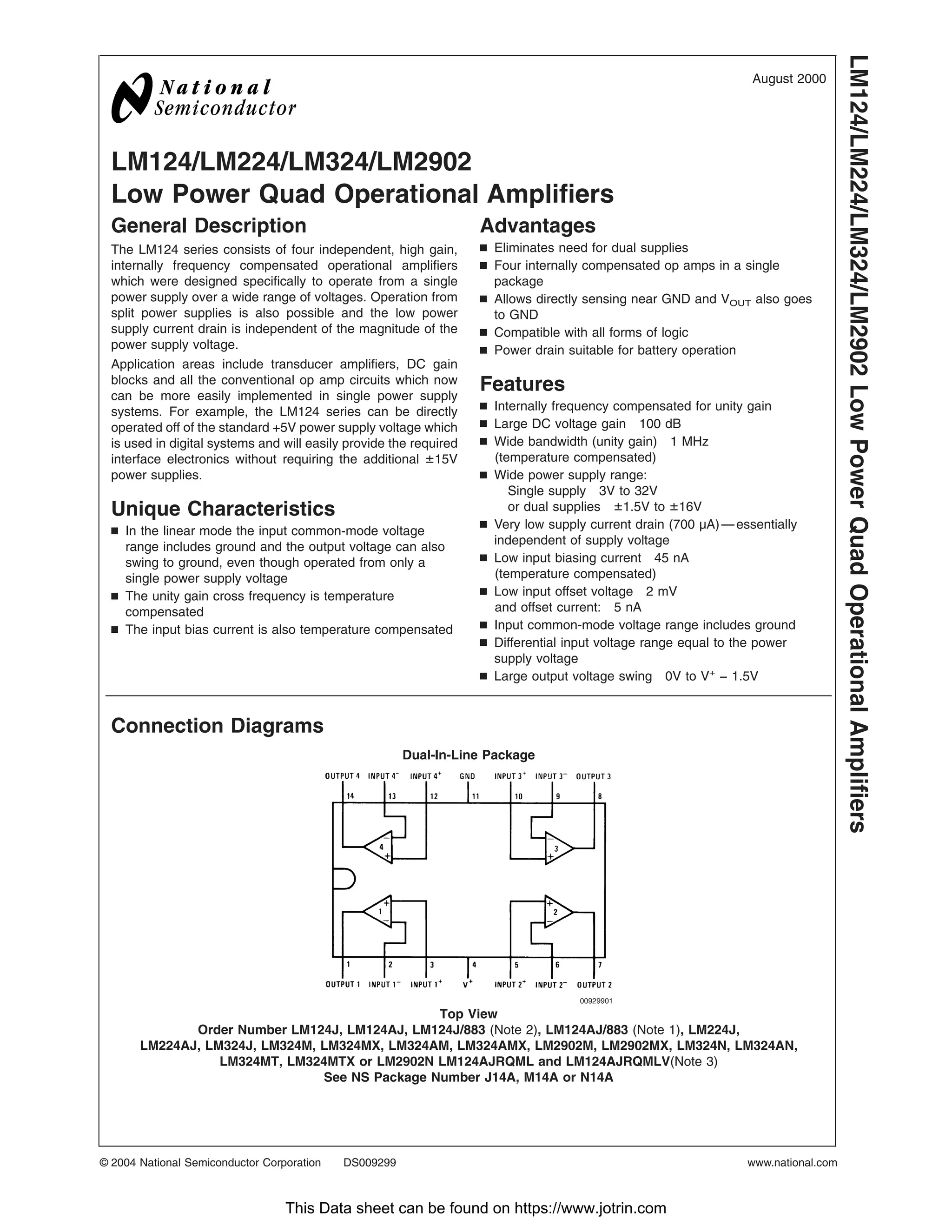
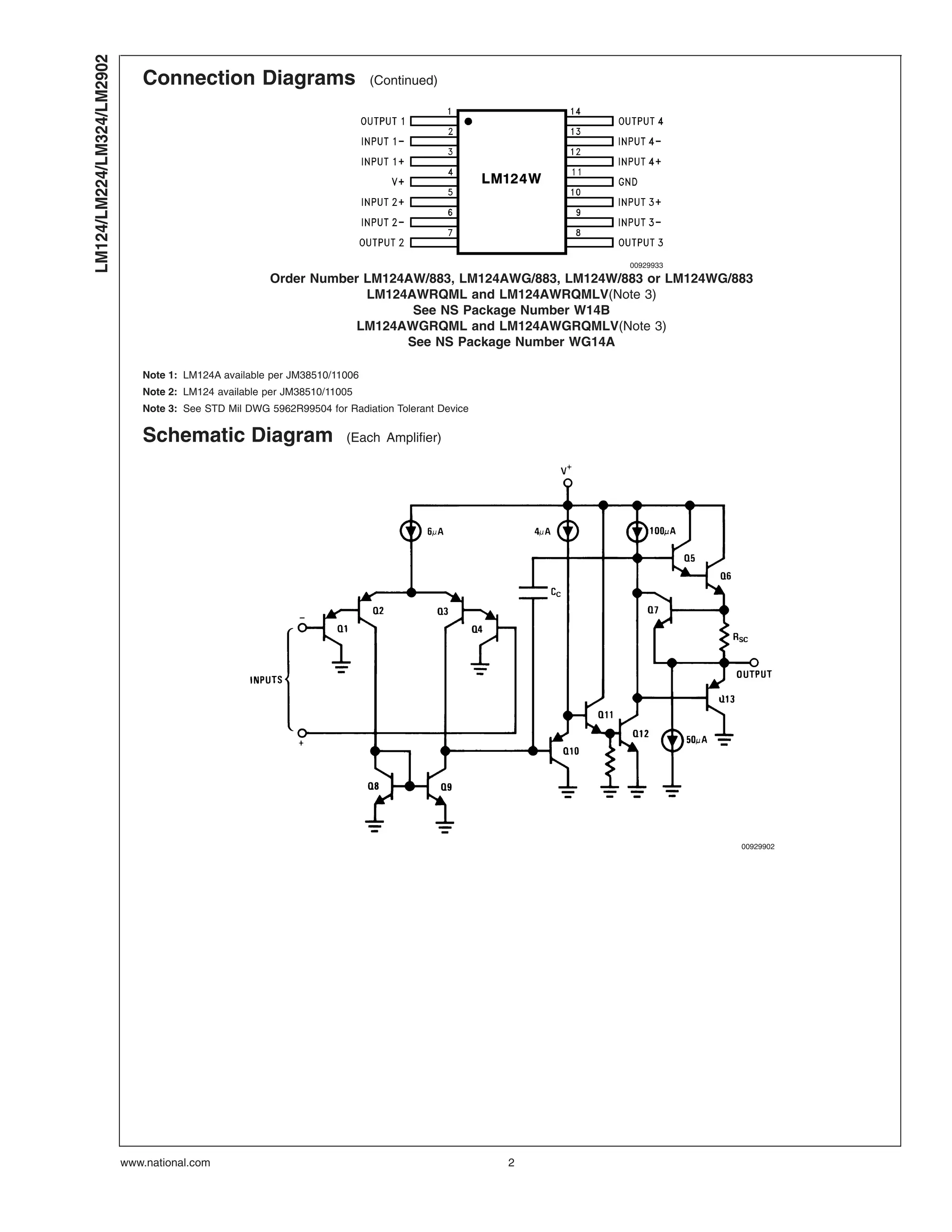
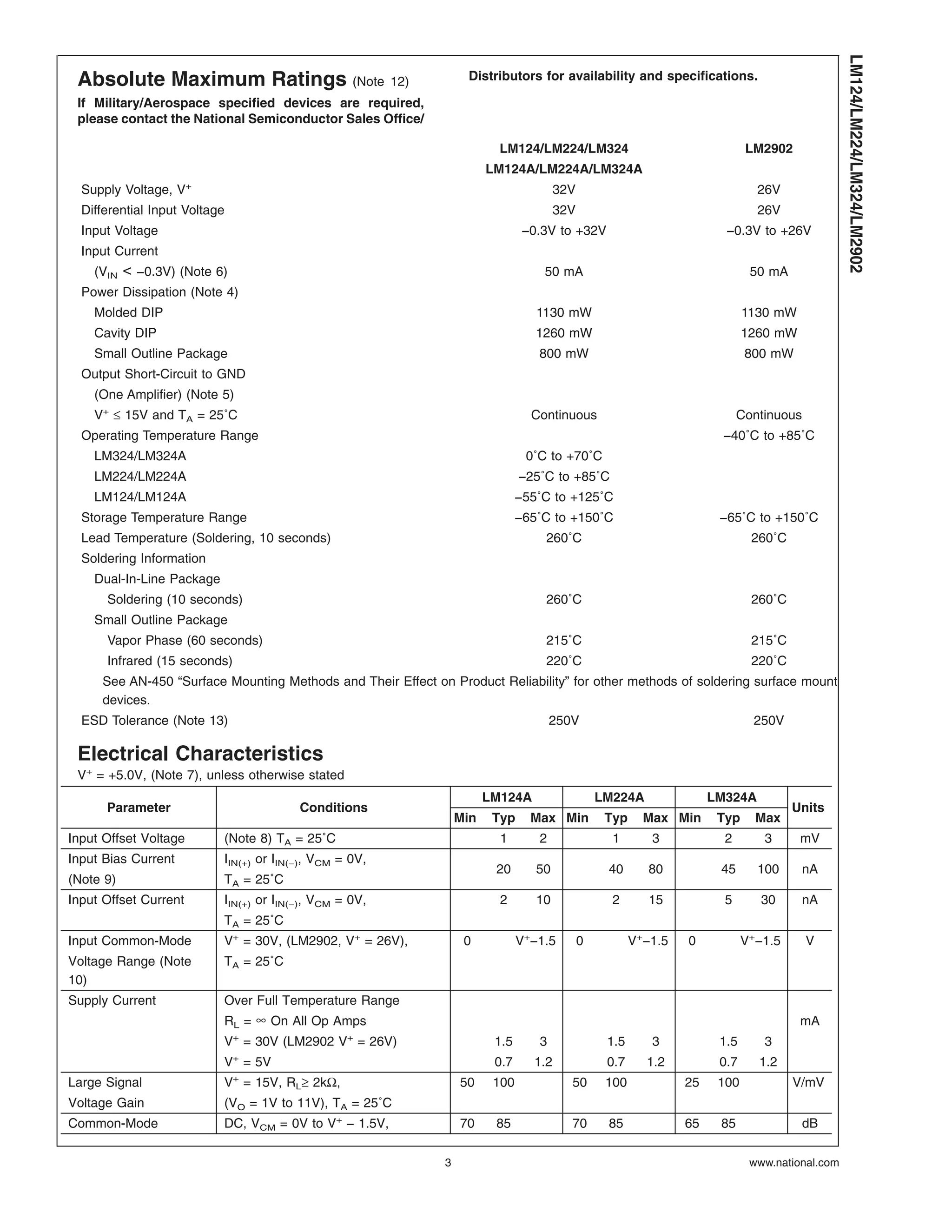
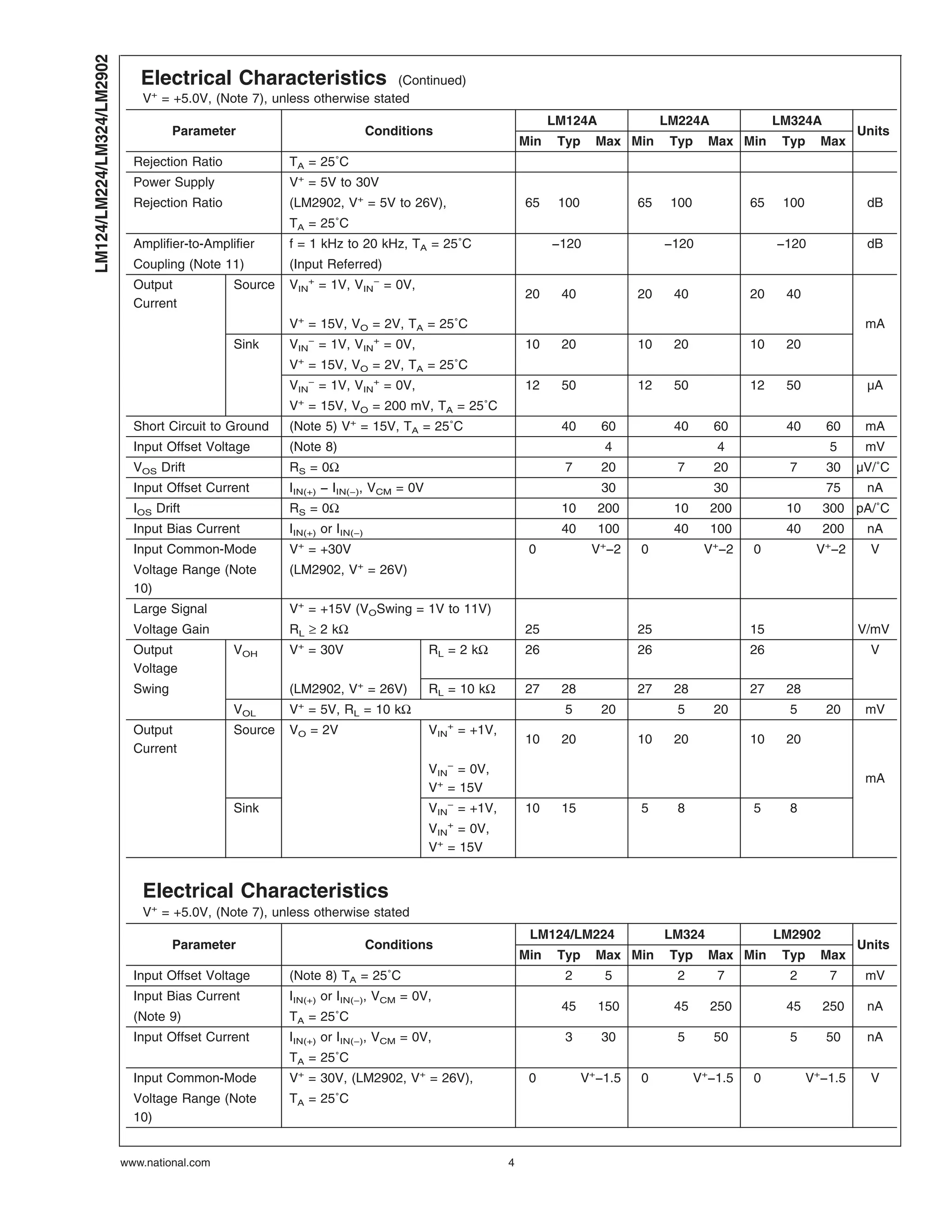
The LM124 series consists of four independent, high gain,
internally frequency compensated operational amplifiers
which were designed specifically to operate from a single
power supply over a wide range of voltages. Operation from
split power supplies is also possible and the low power
supply current drain is independent of the magnitude of the
power supply voltage.
Application areas include transducer amplifiers, DC gain
blocks and all the conventional op amp circuits which now
can be more easily implemented in single power supply
systems. For example, the LM124 series can be directly
operated off of the standard +5V power supply voltage which
is used in digital systems and will easily provide the required
interface electronics without requiring the additional ±15V
power supplies.
Original Driver Mosfet IRS21814STRPBF IRS21814S 21814 SOP-14 New Internationa...AUTHELECTRONIC
Original Driver Mosfet IRS21814STRPBF IRS21814S 21814 SOP-14 New International Rectifier
https://authelectronic.com/original-driver-mosfet-irs21814strpbf-irs21814s-21814-sop-14-new-international-rectifier
Mikro,
Catalog Thiết Bị Điện Mikro, Catalog Thiết Bị Điện,
Catalog Phụ Kiện Mikro, Catalog Phụ Kiện,
Catalog Mikro, Catalog,
http://dienhathe.com,
Chi tiết các sản phẩm khác của Mikro tại https://dienhathe.com
Xem thêm các Catalog khác của Mikro tại https://dienhathe.info
Để nhận báo giá sản phẩm Mikro vui lòng gọi: 0907.764.966
ICL7660 Monolithic CMOS Voltage ConvertersGeorgage Zim
ICL7660 and ICL7660A contain all the necessary circuitry to complete a negative voltage converter, with the exception of 2 external capacitors which may be inexpensive 10μF polarized electrolytic types. Please visit for more information http://www.intersil.com/en/products/power-management/isolated-power/charge-pumps/ICL7660.html
Research on image processing based on fpgaVinsion Chan
Image processing is a technique that uses a computer to analyze images to achieve the desired results, also known as image processing. It is to operate images to get the results you want. It is a very broad concept, including image enhancement, image restoration, image reconstruction, image analysis, pattern recognition, computer vision and other N multiple application directions.
The functional design scheme of the dedicated keyboard chip kb core based on ...Vinsion Chan
In the single-chip application system, there are various forms of external data input interface interfaces, such as RS-232C serial communication, keyboard input, etc.
How to choose the right thermistor for the temperature sensorVinsion Chan
When faced with thousands of thermistor types, selection may cause considerable difficulties. In this technical article, I will introduce you to some important parameters to keep in mind when choosing a thermistor, especially when you want to use two commonly used thermistor types for temperature sensing (negative temperature coefficient NTC thermistor) Resistor or silicon-based linear thermistor). NTC thermistors are widely used because of their low price, but they provide low accuracy at extreme temperatures.
Tda2822 features, pin functions and application circuitsVinsion Chan
TDA2822 is a dual-channel monolithic power amplifier integrated circuit developed by STMicroelectronics (ST). It has the characteristics of a simple circuit, good sound quality, and a wide voltage range.
Udn2916 lb performance characteristics and application circuit analysisVinsion Chan
With the further advancement of the "Golden Tax" project, in 2005 nearly 100 enterprises obtained tax-controlled cash register production licenses, and the tax-controlled market with a capacity of 30 million units is about to blow out. It is estimated that about one-third of the tax-controlled cash register market will install dual-step micro printers to print invoices. The UDN2916LB driving chip for controlling this type of stepper motor will be widely used in the market.
Quickly design infrared body temperature detectorVinsion Chan
Body temperature testing is necessary monitoring in our homes, in and out of the community or workplace, and during travel. Infrared body temperature detector helps reduce contact infection through non-contact temperature measurement. Here we come to talk to you about this system and the main design plan.
Operation and maintenance of power capacitorsVinsion Chan
Power capacitor is a kind of static reactive power compensation equipment. Its main role is to provide reactive power to the power system and improve the power factor.
Frequency hopping signal of dds based on fpga hardwareVinsion Chan
Design of Frequency-hopping Signal Generation System for DDS Based on FPGA Hardware. Frequency-hopping communication has good anti-interference, anti-multipath fading, anti-interception capabilities, and fast synchronization. It is widely used in military, transportation, commercial and other fields
Will the largest acquisition in the semiconductorVinsion Chan
In recent years, Microsemi has grown through a series of mergers and acquisitions, especially in the aerospace and defense fields. Microsemi hopes to further expand in the aerospace and defense fields through this transaction. As a buyer, Microchip currently has a relatively weak sense of presence in the aerospace and defense markets, accounting for only about 2% of its annual sales
UiPath Test Automation using UiPath Test Suite series, part 4DianaGray10
Welcome to UiPath Test Automation using UiPath Test Suite series part 4. In this session, we will cover Test Manager overview along with SAP heatmap.
The UiPath Test Manager overview with SAP heatmap webinar offers a concise yet comprehensive exploration of the role of a Test Manager within SAP environments, coupled with the utilization of heatmaps for effective testing strategies.
Participants will gain insights into the responsibilities, challenges, and best practices associated with test management in SAP projects. Additionally, the webinar delves into the significance of heatmaps as a visual aid for identifying testing priorities, areas of risk, and resource allocation within SAP landscapes. Through this session, attendees can expect to enhance their understanding of test management principles while learning practical approaches to optimize testing processes in SAP environments using heatmap visualization techniques
What will you get from this session?
1. Insights into SAP testing best practices
2. Heatmap utilization for testing
3. Optimization of testing processes
4. Demo
Topics covered:
Execution from the test manager
Orchestrator execution result
Defect reporting
SAP heatmap example with demo
Speaker:
Deepak Rai, Automation Practice Lead, Boundaryless Group and UiPath MVP
Accelerate your Kubernetes clusters with Varnish CachingThijs Feryn
A presentation about the usage and availability of Varnish on Kubernetes. This talk explores the capabilities of Varnish caching and shows how to use the Varnish Helm chart to deploy it to Kubernetes.
This presentation was delivered at K8SUG Singapore. See https://feryn.eu/presentations/accelerate-your-kubernetes-clusters-with-varnish-caching-k8sug-singapore-28-2024 for more details.
Connector Corner: Automate dynamic content and events by pushing a buttonDianaGray10
Here is something new! In our next Connector Corner webinar, we will demonstrate how you can use a single workflow to:
Create a campaign using Mailchimp with merge tags/fields
Send an interactive Slack channel message (using buttons)
Have the message received by managers and peers along with a test email for review
But there’s more:
In a second workflow supporting the same use case, you’ll see:
Your campaign sent to target colleagues for approval
If the “Approve” button is clicked, a Jira/Zendesk ticket is created for the marketing design team
But—if the “Reject” button is pushed, colleagues will be alerted via Slack message
Join us to learn more about this new, human-in-the-loop capability, brought to you by Integration Service connectors.
And...
Speakers:
Akshay Agnihotri, Product Manager
Charlie Greenberg, Host
Kubernetes & AI - Beauty and the Beast !?! @KCD Istanbul 2024Tobias Schneck
As AI technology is pushing into IT I was wondering myself, as an “infrastructure container kubernetes guy”, how get this fancy AI technology get managed from an infrastructure operational view? Is it possible to apply our lovely cloud native principals as well? What benefit’s both technologies could bring to each other?
Let me take this questions and provide you a short journey through existing deployment models and use cases for AI software. On practical examples, we discuss what cloud/on-premise strategy we may need for applying it to our own infrastructure to get it to work from an enterprise perspective. I want to give an overview about infrastructure requirements and technologies, what could be beneficial or limiting your AI use cases in an enterprise environment. An interactive Demo will give you some insides, what approaches I got already working for real.
The Art of the Pitch: WordPress Relationships and SalesLaura Byrne
Clients don’t know what they don’t know. What web solutions are right for them? How does WordPress come into the picture? How do you make sure you understand scope and timeline? What do you do if sometime changes?
All these questions and more will be explored as we talk about matching clients’ needs with what your agency offers without pulling teeth or pulling your hair out. Practical tips, and strategies for successful relationship building that leads to closing the deal.
UiPath Test Automation using UiPath Test Suite series, part 3DianaGray10
Welcome to UiPath Test Automation using UiPath Test Suite series part 3. In this session, we will cover desktop automation along with UI automation.
Topics covered:
UI automation Introduction,
UI automation Sample
Desktop automation flow
Pradeep Chinnala, Senior Consultant Automation Developer @WonderBotz and UiPath MVP
Deepak Rai, Automation Practice Lead, Boundaryless Group and UiPath MVP
DevOps and Testing slides at DASA ConnectKari Kakkonen
My and Rik Marselis slides at 30.5.2024 DASA Connect conference. We discuss about what is testing, then what is agile testing and finally what is Testing in DevOps. Finally we had lovely workshop with the participants trying to find out different ways to think about quality and testing in different parts of the DevOps infinity loop.
Smart TV Buyer Insights Survey 2024 by 91mobiles.pdf91mobiles
91mobiles recently conducted a Smart TV Buyer Insights Survey in which we asked over 3,000 respondents about the TV they own, aspects they look at on a new TV, and their TV buying preferences.
Generating a custom Ruby SDK for your web service or Rails API using Smithyg2nightmarescribd
Have you ever wanted a Ruby client API to communicate with your web service? Smithy is a protocol-agnostic language for defining services and SDKs. Smithy Ruby is an implementation of Smithy that generates a Ruby SDK using a Smithy model. In this talk, we will explore Smithy and Smithy Ruby to learn how to generate custom feature-rich SDKs that can communicate with any web service, such as a Rails JSON API.
Epistemic Interaction - tuning interfaces to provide information for AI supportAlan Dix
Paper presented at SYNERGY workshop at AVI 2024, Genoa, Italy. 3rd June 2024
https://alandix.com/academic/papers/synergy2024-epistemic/
As machine learning integrates deeper into human-computer interactions, the concept of epistemic interaction emerges, aiming to refine these interactions to enhance system adaptability. This approach encourages minor, intentional adjustments in user behaviour to enrich the data available for system learning. This paper introduces epistemic interaction within the context of human-system communication, illustrating how deliberate interaction design can improve system understanding and adaptation. Through concrete examples, we demonstrate the potential of epistemic interaction to significantly advance human-computer interaction by leveraging intuitive human communication strategies to inform system design and functionality, offering a novel pathway for enriching user-system engagements.
GDG Cloud Southlake #33: Boule & Rebala: Effective AppSec in SDLC using Deplo...James Anderson
Effective Application Security in Software Delivery lifecycle using Deployment Firewall and DBOM
The modern software delivery process (or the CI/CD process) includes many tools, distributed teams, open-source code, and cloud platforms. Constant focus on speed to release software to market, along with the traditional slow and manual security checks has caused gaps in continuous security as an important piece in the software supply chain. Today organizations feel more susceptible to external and internal cyber threats due to the vast attack surface in their applications supply chain and the lack of end-to-end governance and risk management.
The software team must secure its software delivery process to avoid vulnerability and security breaches. This needs to be achieved with existing tool chains and without extensive rework of the delivery processes. This talk will present strategies and techniques for providing visibility into the true risk of the existing vulnerabilities, preventing the introduction of security issues in the software, resolving vulnerabilities in production environments quickly, and capturing the deployment bill of materials (DBOM).
Speakers:
Bob Boule
Robert Boule is a technology enthusiast with PASSION for technology and making things work along with a knack for helping others understand how things work. He comes with around 20 years of solution engineering experience in application security, software continuous delivery, and SaaS platforms. He is known for his dynamic presentations in CI/CD and application security integrated in software delivery lifecycle.
Gopinath Rebala
Gopinath Rebala is the CTO of OpsMx, where he has overall responsibility for the machine learning and data processing architectures for Secure Software Delivery. Gopi also has a strong connection with our customers, leading design and architecture for strategic implementations. Gopi is a frequent speaker and well-known leader in continuous delivery and integrating security into software delivery.
Securing your Kubernetes cluster_ a step-by-step guide to success !KatiaHIMEUR1
Today, after several years of existence, an extremely active community and an ultra-dynamic ecosystem, Kubernetes has established itself as the de facto standard in container orchestration. Thanks to a wide range of managed services, it has never been so easy to set up a ready-to-use Kubernetes cluster.
However, this ease of use means that the subject of security in Kubernetes is often left for later, or even neglected. This exposes companies to significant risks.
In this talk, I'll show you step-by-step how to secure your Kubernetes cluster for greater peace of mind and reliability.
2. Connection Diagrams (Continued)
00929933
Order Number LM124AW/883, LM124AWG/883, LM124W/883 or LM124WG/883
LM124AWRQML and LM124AWRQMLV(Note 3)
See NS Package Number W14B
LM124AWGRQML and LM124AWGRQMLV(Note 3)
See NS Package Number WG14A
Note 1: LM124A available per JM38510/11006
Note 2: LM124 available per JM38510/11005
Note 3: See STD Mil DWG 5962R99504 for Radiation Tolerant Device
Schematic Diagram (Each Amplifier)
00929902
LM124/LM224/LM324/LM2902
www.national.com 2
3. Absolute Maximum Ratings (Note 12)
If Military/Aerospace specified devices are required,
please contact the National Semiconductor Sales Office/
Distributors for availability and specifications.
LM124/LM224/LM324 LM2902
LM124A/LM224A/LM324A
Supply Voltage, V+
32V 26V
Differential Input Voltage 32V 26V
Input Voltage −0.3V to +32V −0.3V to +26V
Input Current
(VIN < −0.3V) (Note 6) 50 mA 50 mA
Power Dissipation (Note 4)
Molded DIP 1130 mW 1130 mW
Cavity DIP 1260 mW 1260 mW
Small Outline Package 800 mW 800 mW
Output Short-Circuit to GND
(One Amplifier) (Note 5)
V+
≤ 15V and TA = 25˚C Continuous Continuous
Operating Temperature Range −40˚C to +85˚C
LM324/LM324A 0˚C to +70˚C
LM224/LM224A −25˚C to +85˚C
LM124/LM124A −55˚C to +125˚C
Storage Temperature Range −65˚C to +150˚C −65˚C to +150˚C
Lead Temperature (Soldering, 10 seconds) 260˚C 260˚C
Soldering Information
Dual-In-Line Package
Soldering (10 seconds) 260˚C 260˚C
Small Outline Package
Vapor Phase (60 seconds) 215˚C 215˚C
Infrared (15 seconds) 220˚C 220˚C
See AN-450 “Surface Mounting Methods and Their Effect on Product Reliability” for other methods of soldering surface mount
devices.
ESD Tolerance (Note 13) 250V 250V
Electrical Characteristics
V+
= +5.0V, (Note 7), unless otherwise stated
Parameter Conditions
LM124A LM224A LM324A
Units
Min Typ Max Min Typ Max Min Typ Max
Input Offset Voltage (Note 8) TA = 25˚C 1 2 1 3 2 3 mV
Input Bias Current IIN(+) or IIN(−), VCM = 0V,
20 50 40 80 45 100 nA
(Note 9) TA = 25˚C
Input Offset Current IIN(+) or IIN(−), VCM = 0V, 2 10 2 15 5 30 nA
TA = 25˚C
Input Common-Mode V+
= 30V, (LM2902, V+
= 26V), 0 V+
−1.5 0 V+
−1.5 0 V+
−1.5 V
Voltage Range (Note
10)
TA = 25˚C
Supply Current Over Full Temperature Range
RL = ∞ On All Op Amps mA
V+
= 30V (LM2902 V+
= 26V) 1.5 3 1.5 3 1.5 3
V+
= 5V 0.7 1.2 0.7 1.2 0.7 1.2
Large Signal V+
= 15V, RL≥ 2kΩ, 50 100 50 100 25 100 V/mV
Voltage Gain (VO = 1V to 11V), TA = 25˚C
Common-Mode DC, VCM = 0V to V+
− 1.5V, 70 85 70 85 65 85 dB
LM124/LM224/LM324/LM2902
www.national.com3
4. Electrical Characteristics (Continued)
V+
= +5.0V, (Note 7), unless otherwise stated
Parameter Conditions
LM124A LM224A LM324A
Units
Min Typ Max Min Typ Max Min Typ Max
Rejection Ratio TA = 25˚C
Power Supply V+
= 5V to 30V
Rejection Ratio (LM2902, V+
= 5V to 26V), 65 100 65 100 65 100 dB
TA = 25˚C
Amplifier-to-Amplifier f = 1 kHz to 20 kHz, TA = 25˚C −120 −120 −120 dB
Coupling (Note 11) (Input Referred)
Output
Current
Source VIN
+
= 1V, VIN
−
= 0V,
20 40 20 40 20 40
V+
= 15V, VO = 2V, TA = 25˚C mA
Sink VIN
−
= 1V, VIN
+
= 0V, 10 20 10 20 10 20
V+
= 15V, VO = 2V, TA = 25˚C
VIN
−
= 1V, VIN
+
= 0V, 12 50 12 50 12 50 µA
V+
= 15V, VO = 200 mV, TA = 25˚C
Short Circuit to Ground (Note 5) V+
= 15V, TA = 25˚C 40 60 40 60 40 60 mA
Input Offset Voltage (Note 8) 4 4 5 mV
VOS Drift RS = 0Ω 7 20 7 20 7 30 µV/˚C
Input Offset Current IIN(+) − IIN(−), VCM = 0V 30 30 75 nA
IOS Drift RS = 0Ω 10 200 10 200 10 300 pA/˚C
Input Bias Current IIN(+) or IIN(−) 40 100 40 100 40 200 nA
Input Common-Mode V+
= +30V 0 V+
−2 0 V+
−2 0 V+
−2 V
Voltage Range (Note
10)
(LM2902, V+
= 26V)
Large Signal V+
= +15V (VOSwing = 1V to 11V)
Voltage Gain RL ≥ 2 kΩ 25 25 15 V/mV
Output
Voltage
VOH V+
= 30V RL = 2 kΩ 26 26 26 V
Swing (LM2902, V+
= 26V) RL = 10 kΩ 27 28 27 28 27 28
VOL V+
= 5V, RL = 10 kΩ 5 20 5 20 5 20 mV
Output
Current
Source VO = 2V VIN
+
= +1V,
10 20 10 20 10 20
VIN
−
= 0V,
V+
= 15V
mA
Sink VIN
−
= +1V, 10 15 5 8 5 8
VIN
+
= 0V,
V+
= 15V
Electrical Characteristics
V+
= +5.0V, (Note 7), unless otherwise stated
Parameter Conditions
LM124/LM224 LM324 LM2902
Units
Min Typ Max Min Typ Max Min Typ Max
Input Offset Voltage (Note 8) TA = 25˚C 2 5 2 7 2 7 mV
Input Bias Current IIN(+) or IIN(−), VCM = 0V,
45 150 45 250 45 250 nA
(Note 9) TA = 25˚C
Input Offset Current IIN(+) or IIN(−), VCM = 0V, 3 30 5 50 5 50 nA
TA = 25˚C
Input Common-Mode V+
= 30V, (LM2902, V+
= 26V), 0 V+
−1.5 0 V+
−1.5 0 V+
−1.5 V
Voltage Range (Note
10)
TA = 25˚C
LM124/LM224/LM324/LM2902
www.national.com 4
5. Electrical Characteristics (Continued)
V+
= +5.0V, (Note 7), unless otherwise stated
Parameter Conditions
LM124/LM224 LM324 LM2902
Units
Min Typ Max Min Typ Max Min Typ Max
Supply Current Over Full Temperature Range
RL = ∞ On All Op Amps mA
V+
= 30V (LM2902 V+
= 26V) 1.5 3 1.5 3 1.5 3
V+
= 5V 0.7 1.2 0.7 1.2 0.7 1.2
Large Signal V+
= 15V, RL≥ 2kΩ, 50 100 25 100 25 100 V/mV
Voltage Gain (VO = 1V to 11V), TA = 25˚C
Common-Mode DC, VCM = 0V to V+
− 1.5V, 70 85 65 85 50 70 dB
Rejection Ratio TA = 25˚C
Power Supply V+
= 5V to 30V
Rejection Ratio (LM2902, V+
= 5V to 26V), 65 100 65 100 50 100 dB
TA = 25˚C
Amplifier-to-Amplifier f = 1 kHz to 20 kHz, TA = 25˚C −120 −120 −120 dB
Coupling (Note 11) (Input Referred)
Output
Current
Source VIN
+
= 1V, VIN
−
= 0V,
20 40 20 40 20 40
V+
= 15V, VO = 2V, TA = 25˚C mA
Sink VIN
−
= 1V, VIN
+
= 0V, 10 20 10 20 10 20
V+
= 15V, VO = 2V, TA = 25˚C
VIN
−
= 1V, VIN
+
= 0V, 12 50 12 50 12 50 µA
V+
= 15V, VO = 200 mV, TA = 25˚C
Short Circuit to Ground (Note 5) V+
= 15V, TA = 25˚C 40 60 40 60 40 60 mA
Input Offset Voltage (Note 8) 7 9 10 mV
VOS Drift RS = 0Ω 7 7 7 µV/˚C
Input Offset Current IIN(+) − IIN(−), VCM = 0V 100 150 45 200 nA
IOS Drift RS = 0Ω 10 10 10 pA/˚C
Input Bias Current IIN(+) or IIN(−) 40 300 40 500 40 500 nA
Input Common-Mode V+
= +30V 0 V+
−2 0 V+
−2 0 V+
−2 V
Voltage Range (Note
10)
(LM2902, V+
= 26V)
Large Signal V+
= +15V (VOSwing = 1V to 11V)
Voltage Gain RL ≥ 2 kΩ 25 15 15 V/mV
Output
Voltage
VOH V+
= 30V RL = 2 kΩ 26 26 22 V
Swing (LM2902, V+
= 26V) RL = 10 kΩ 27 28 27 28 23 24
VOL V+
= 5V, RL = 10 kΩ 5 20 5 20 5 100 mV
Output
Current
Source VO = 2V VIN
+
= +1V,
10 20 10 20 10 20
VIN
−
= 0V,
V+
= 15V
mA
Sink VIN
−
= +1V, 5 8 5 8 5 8
VIN
+
= 0V,
V+
= 15V
Note 4: For operating at high temperatures, the LM324/LM324A/LM2902 must be derated based on a +125˚C maximum junction temperature and a thermal
resistance of 88˚C/W which applies for the device soldered in a printed circuit board, operating in a still air ambient. The LM224/LM224A and LM124/LM124A can
be derated based on a +150˚C maximum junction temperature. The dissipation is the total of all four amplifiers — use external resistors, where possible, to allow the
amplifier to saturate of to reduce the power which is dissipated in the integrated circuit.
Note 5: Short circuits from the output to V+
can cause excessive heating and eventual destruction. When considering short circuits to ground, the maximum output
current is approximately 40 mA independent of the magnitude of V+. At values of supply voltage in excess of +15V, continuous short-circuits can exceed the power
dissipation ratings and cause eventual destruction. Destructive dissipation can result from simultaneous shorts on all amplifiers.
Note 6: This input current will only exist when the voltage at any of the input leads is driven negative. It is due to the collector-base junction of the input PNP
transistors becoming forward biased and thereby acting as input diode clamps. In addition to this diode action, there is also lateral NPN parasitic transistor action
LM124/LM224/LM324/LM2902
www.national.com5
6. Electrical Characteristics (Continued)
on the IC chip. This transistor action can cause the output voltages of the op amps to go to the V+
voltage level (or to ground for a large overdrive) for the time duration
that an input is driven negative. This is not destructive and normal output states will re-establish when the input voltage, which was negative, again returns to a value
greater than −0.3V (at 25˚C).
Note 7: These specifications are limited to −55˚C ≤ TA ≤ +125˚C for the LM124/LM124A. With the LM224/LM224A, all temperature specifications are limited to
−25˚C ≤ TA ≤ +85˚C, the LM324/LM324A temperature specifications are limited to 0˚C ≤ TA ≤ +70˚C, and the LM2902 specifications are limited to −40˚C ≤ TA ≤
+85˚C.
Note 8: VO . 1.4V, RS = 0Ω with V+ from 5V to 30V; and over the full input common-mode range (0V to V+ − 1.5V) for LM2902, V+ from 5V to 26V.
Note 9: The direction of the input current is out of the IC due to the PNP input stage. This current is essentially constant, independent of the state of the output so
no loading change exists on the input lines.
Note 10: The input common-mode voltage of either input signal voltage should not be allowed to go negative by more than 0.3V (at 25˚C). The upper end of the
common-mode voltage range is V+ − 1.5V (at 25˚C), but either or both inputs can go to +32V without damage (+26V for LM2902), independent of the magnitude
of V+.
Note 11: Due to proximity of external components, insure that coupling is not originating via stray capacitance between these external parts. This typically can be
detected as this type of capacitance increases at higher frequencies.
Note 12: Refer to RETS124AX for LM124A military specifications and refer to RETS124X for LM124 military specifications.
Note 13: Human body model, 1.5 kΩ in series with 100 pF.
Typical Performance Characteristics
Input Voltage Range Input Current
00929934 00929935
Supply Current Voltage Gain
00929936 00929937
LM124/LM224/LM324/LM2902
www.national.com 6
7. Typical Performance Characteristics (Continued)
Open Loop Frequency
Response
Common Mode Rejection
Ratio
00929938
00929939
Voltage Follower Pulse
Response
Voltage Follower Pulse
Response (Small Signal)
00929940 00929941
Large Signal Frequency
Response
Output Characteristics
Current Sourcing
00929942 00929943
LM124/LM224/LM324/LM2902
www.national.com7
8. Typical Performance Characteristics (Continued)
Output Characteristics
Current Sinking Current Limiting
00929944 00929945
Input Current (LM2902 only) Voltage Gain (LM2902 only)
00929946 00929947
Application Hints
The LM124 series are op amps which operate with only a
single power supply voltage, have true-differential inputs,
and remain in the linear mode with an input common-mode
voltage of 0 VDC. These amplifiers operate over a wide range
of power supply voltage with little change in performance
characteristics. At 25˚C amplifier operation is possible down
to a minimum supply voltage of 2.3 VDC.
The pinouts of the package have been designed to simplify
PC board layouts. Inverting inputs are adjacent to outputs for
all of the amplifiers and the outputs have also been placed at
the corners of the package (pins 1, 7, 8, and 14).
Precautions should be taken to insure that the power supply
for the integrated circuit never becomes reversed in polarity
or that the unit is not inadvertently installed backwards in a
test socket as an unlimited current surge through the result-
ing forward diode within the IC could cause fusing of the
internal conductors and result in a destroyed unit.
Large differential input voltages can be easily accommo-
dated and, as input differential voltage protection diodes are
not needed, no large input currents result from large differ-
ential input voltages. The differential input voltage may be
larger than V+
without damaging the device. Protection
should be provided to prevent the input voltages from going
negative more than −0.3 VDC (at 25˚C). An input clamp diode
with a resistor to the IC input terminal can be used.
To reduce the power supply drain, the amplifiers have a
class A output stage for small signal levels which converts to
class B in a large signal mode. This allows the amplifiers to
both source and sink large output currents. Therefore both
NPN and PNP external current boost transistors can be used
to extend the power capability of the basic amplifiers. The
output voltage needs to raise approximately 1 diode drop
above ground to bias the on-chip vertical PNP transistor for
output current sinking applications.
For ac applications, where the load is capacitively coupled to
the output of the amplifier, a resistor should be used, from
the output of the amplifier to ground to increase the class A
bias current and prevent crossover distortion.
Where the load is directly coupled, as in dc applications,
there is no crossover distortion.
Capacitive loads which are applied directly to the output of
the amplifier reduce the loop stability margin. Values of
50 pF can be accommodated using the worst-case non-
inverting unity gain connection. Large closed loop gains or
resistive isolation should be used if larger load capacitance
must be driven by the amplifier.
LM124/LM224/LM324/LM2902
www.national.com 8
9. Application Hints (Continued)
The bias network of the LM124 establishes a drain current
which is independent of the magnitude of the power supply
voltage over the range of from 3 VDC to 30 VDC.
Output short circuits either to ground or to the positive power
supply should be of short time duration. Units can be de-
stroyed, not as a result of the short circuit current causing
metal fusing, but rather due to the large increase in IC chip
dissipation which will cause eventual failure due to exces-
sive junction temperatures. Putting direct short-circuits on
more than one amplifier at a time will increase the total IC
power dissipation to destructive levels, if not properly pro-
tected with external dissipation limiting resistors in series
with the output leads of the amplifiers. The larger value of
output source current which is available at 25˚C provides a
larger output current capability at elevated temperatures
(see typical performance characteristics) than a standard IC
op amp.
The circuits presented in the section on typical applications
emphasize operation on only a single power supply voltage.
If complementary power supplies are available, all of the
standard op amp circuits can be used. In general, introduc-
ing a pseudo-ground (a bias voltage reference of V+
/2) will
allow operation above and below this value in single power
supply systems. Many application circuits are shown which
take advantage of the wide input common-mode voltage
range which includes ground. In most cases, input biasing is
not required and input voltages which range to ground can
easily be accommodated.
Typical Single-Supply Applications (V+
= 5.0 VDC)
Non-Inverting DC Gain (0V Input = 0V Output)
00929905
*R not needed due to temperature independent IIN
DC Summing Amplifier
(VIN’S ≥ 0 VDC and VO ≥ VDC) Power Amplifier
00929906
Where: V0 = V1 + V2 − V3 − V4
(V1 + V2) ≥ (V3 + V4) to keep VO > 0 VDC
00929907
V0 = 0 VDC for VIN = 0 VDC
AV = 10
LM124/LM224/LM324/LM2902
www.national.com9
10. Typical Single-Supply Applications (V+
= 5.0 VDC) (Continued)
LED Driver “BI-QUAD” RC Active Bandpass Filter
00929908
00929909
fo = 1 kHz
Q = 50
AV = 100 (40 dB)
Fixed Current Sources Lamp Driver
00929910
00929911
LM124/LM224/LM324/LM2902
www.national.com 10
11. Typical Single-Supply Applications
(V+ = 5.0 VDC) (Continued)
Current Monitor
00929912
*(Increase R1 for IL small)
Driving TTL
00929913
Voltage Follower
00929914
Pulse Generator
00929915
Squarewave Oscillator
00929916
Pulse Generator
00929917
LM124/LM224/LM324/LM2902
www.national.com11
12. Typical Single-Supply Applications (V+
= 5.0 VDC) (Continued)
High Compliance Current Sink
00929918
IO = 1 amp/volt VIN
(Increase RE for Io small)
Low Drift Peak Detector
00929919
LM124/LM224/LM324/LM2902
www.national.com 12
13. Typical Single-Supply Applications (V+
= 5.0 VDC) (Continued)
Comparator with Hysteresis Ground Referencing a Differential Input Signal
00929920
00929921
VO = VR
Voltage Controlled Oscillator Circuit
00929922
*Wide control voltage range: 0 VDC ≤ VC ≤ 2 (V+
−1.5 VDC)
Photo Voltaic-Cell Amplifier
00929923
LM124/LM224/LM324/LM2902
www.national.com13
15. Typical Single-Supply Applications (V+
= 5.0 VDC) (Continued)
DC Coupled Low-Pass RC Active Filter
00929926
fO = 1 kHz
Q = 1
AV = 2
High Input Z, DC Differential Amplifier
00929927
LM124/LM224/LM324/LM2902
www.national.com15
16. Typical Single-Supply Applications (V+
= 5.0 VDC) (Continued)
High Input Z Adjustable-Gain
DC Instrumentation Amplifier
00929928
Using Symmetrical Amplifiers to
Reduce Input Current (General Concept)
00929929
Bridge Current Amplifier
00929930
LM124/LM224/LM324/LM2902
www.national.com 16
18. Physical Dimensions inches (millimeters) unless otherwise noted
Ceramic Dual-In-Line Package (J)
Order Number JL124ABCA, JL124BCA, JL124ASCA, JL124SCA, LM124J,
LM124AJ, LM124AJ/883, LM124J/883, LM224J, LM224AJ or LM324J
NS Package Number J14A
MX S.O. Package (M)
Order Number LM324M, LM324MX, LM324AM, LM324AMX, LM2902M or LM2902MX
NS Package Number M14A
LM124/LM224/LM324/LM2902
www.national.com 18
19. Physical Dimensions inches (millimeters) unless otherwise noted (Continued)
Molded Dual-In-Line Package (N)
Order Number LM324N, LM324AN or LM2902N
NS Package Number N14A
Ceramic Flatpak Package
Order Number JL124ABDA, JL124ABZA, JL124ASDA, JL124BDA, JL124BZA,
JL124SDA, LM124AW/883, LM124AWG/883, LM124W/883 or LM124WG/883
NS Package Number W14B
LM124/LM224/LM324/LM2902
www.national.com19
20. Physical Dimensions inches (millimeters) unless otherwise noted (Continued)
14-Pin TSSOP
Order NumberLM324MT or LM324MTX
NS Package Number MTC14
LIFE SUPPORT POLICY
NATIONAL’S PRODUCTS ARE NOT AUTHORIZED FOR USE AS CRITICAL COMPONENTS IN LIFE SUPPORT
DEVICES OR SYSTEMS WITHOUT THE EXPRESS WRITTEN APPROVAL OF THE PRESIDENT AND GENERAL
COUNSEL OF NATIONAL SEMICONDUCTOR CORPORATION. As used herein:
1. Life support devices or systems are devices or
systems which, (a) are intended for surgical implant
into the body, or (b) support or sustain life, and
whose failure to perform when properly used in
accordance with instructions for use provided in the
labeling, can be reasonably expected to result in a
significant injury to the user.
2. A critical component is any component of a life
support device or system whose failure to perform
can be reasonably expected to cause the failure of
the life support device or system, or to affect its
safety or effectiveness.
BANNED SUBSTANCE COMPLIANCE
National Semiconductor certifies that the products and packing materials meet the provisions of the Customer Products
Stewardship Specification (CSP-9-111C2) and the Banned Substances and Materials of Interest Specification
(CSP-9-111S2) and contain no ‘‘Banned Substances’’ as defined in CSP-9-111S2.
National Semiconductor
Americas Customer
Support Center
Email: new.feedback@nsc.com
Tel: 1-800-272-9959
National Semiconductor
Europe Customer Support Center
Fax: +49 (0) 180-530 85 86
Email: europe.support@nsc.com
Deutsch Tel: +49 (0) 69 9508 6208
English Tel: +44 (0) 870 24 0 2171
Français Tel: +33 (0) 1 41 91 8790
National Semiconductor
Asia Pacific Customer
Support Center
Email: ap.support@nsc.com
National Semiconductor
Japan Customer Support Center
Fax: 81-3-5639-7507
Email: jpn.feedback@nsc.com
Tel: 81-3-5639-7560
www.national.com
LM124/LM224/LM324/LM2902LowPowerQuadOperationalAmplifiers
National does not assume any responsibility for use of any circuitry described, no circuit patent licenses are implied and National reserves the right at any time without notice to change said circuitry and specifications.