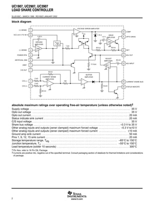
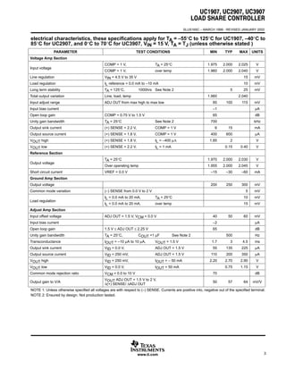
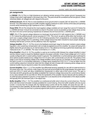
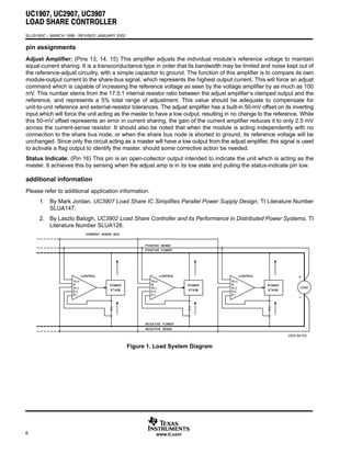
1. UC1907, UC2907, UC3907
LOAD SHARE CONTROLLER
ą
SLUS165C – MARCH 1999 - REVISED JANUARY 2002
1www.ti.com
FEATURES
D Fully Differential High Impedance Voltage
Sensing
D Accurate Current Amplifier for Precise
Current Sharing
D Opto Coupler Driving Capability
D 1.25% Trimmed Reference
D Master Status Indication
D 4.5-V to 35-V Operation
DESCRIPTION
The UCx907 family of load share controller ICs provides all the necessary features to allow
multiple-independent-power modules to be paralleled such that each module supplies only its proportionate share
to total-load current.
This sharing is accomplished by controlling each module’s power stage with a command generated from a
voltage-feedback amplifier whose reference can be independently adjusted in response to a common-share-bus
voltage. By monitoring the current from each module, the current share bus circuitry determines which paralleled
module would normally have the highest output current and, with the designation of this unit as the master, adjusts
all the other modules to increase their output current to within 2.5% of that of the master.
The current share bus signal interconnecting all the paralleled modules is a low-impedance, noise-insensitive line
which will not interfere with allowing each module to act independently should the bus become open or shorted to
ground. The UC3907 controller will reside on the output side of each power module and its overall function is to supply
a voltage feedback loop. The specific architecture of the power stage is unimportant. Either switching or linear designs
may be utilized and the control signal may be either directly coupled or isolated though the use of an optocoupler or
other isolated medium.
Other features of the UC3907 include 1.25% accurate reference: a low-loss, fixed-gain current-sense amplifier, a fully
differential, high-impedance voltage sensing capability, and a status indicator to designate which module is
performing as master.
Copyright 2000, Texas Instruments IncorporatedPRODUCTION DATA information is current as of publication date.
Products conform to specifications per the terms of Texas Instruments
standard warranty. Production processing does not necessarily include
testing of all parameters.
Please be aware that an important notice concerning availability, standard warranty, and use in critical applications of
Texas Instruments semiconductor products and disclaimers thereto appears at the end of this data sheet.
1
2
3
4
5
6
7
8
16
15
14
13
12
11
10
9
C/S OUT
C/S (+)
C/S (–)
(–) SENSE
POWER RETURN
ARTIFICIAL GND
VREF
ISET
STATUS INDICATE
CURRENT SHARE BUS
ADJ OUT
ADJ INPUT
COMP
(+) SENSE
VCC
OPTO DRIVE
DIL-16 J or N PACKAGE
(TOP VIEW)
1
2
3
4
5
6
7
8
16
15
14
13
12
11
10
9
C/S OUT
C/S (+)
C/S (–)
(–) SENSE
POWER RETURN
ARTIFICIAL GND
VREF
ISET
STATUS INDICATE
CURRENT SHARE BUS
ADJ OUT
ADJ INPUT
COMP
(+) SENSE
VCC
OPTO DRIVE
SOIC-16 DW PACKAGE
(TOP VIEW)
192013 2
17
18
16
15
14
1312119 10
5
4
6
7
8
ADJ OUT
ADJ INPUT
N/C
COMP
(+) SENSE
C/S (–)
(–) SENSE
N/C
POWER RETURN
ARTIFICIAL GND
C/S(+)
C/SOUT
N/C
STATUSINDICATE
CURRENTSHAREBUS
ISET
N/C
OPTODRIVE
VCC
VREF
PLCC-20, LCC-20,
Q OR L PACKAGE
(TOP VIEW)
3. UC1907, UC2907, UC3907
LOAD SHARE CONTROLLER
ą
SLUS165C – MARCH 1999 - REVISED JANUARY 2002
3www.ti.com
electrical characteristics, these specifications apply for TA = –55°C to 125°C for UC1907, –40°C to
85°C for UC2907, and 0°C to 70°C for UC3907, VIN = 15 V, TA = TJ (unless otherwise stated )
PARAMETER TEST CONDITIONS MIN TYP MAX UNITS
Voltage Amp Section
Inp t oltage
COMP = 1 V, TA = 25°C 1.975 2.000 2.025 V
Input voltage
COMP = 1 V, over temp 1.960 2.000 2.040 V
Line regulation VIN = 4.5 V to 35 V 15 mV
Load regulation IL reference = 0.0 mA to –10 mA 10 mV
Long term stability TA = 125°C, 1000hrs See Note 2 5 25 mV
Total output variation Line, load, temp 1.960 2.040
Input adjust range ADJ OUT from max high to max low 85 100 115 mV
Input bias current –1 µA
Open loop gain COMP = 0.75 V to 1.5 V 65 dB
Unity gain bandwidth TA = 25°C See Note 2 700 kHz
Output sink current (+) SENSE = 2.2 V, COMP = 1 V 6 15 mA
Output source current (+) SENSE = 1.8 V, COMP = 1 V 400 600 µA
VOUT high (+) SENSE = 1.8 V, IL = –400 µΑ 1.85 2 V
VOUT low (+) SENSE = 2.2 V, IL = 1 mA 0.15 0.40 V
Reference Section
O tp t oltage
TA = 25°C 1.970 2.000 2.030 V
Output voltage
Over operating temp 1.955 2.000 2.045 V
Short circuit current VREF = 0.0 V –15 –30 –60 mA
Ground Amp Section
Output voltage 200 250 300 mV
Common mode variation (–) SENSE from 0.0 V to 2 V 5 mV
Load reg lation
IL = 0.0 mA to 20 mA, TA = 25°C 10 mV
Load regulation
IL = 0.0 mA to 20 mA, over temp 15 mV
Adjust Amp Section
Input offset voltage ADJ OUT = 1.5 V, VCM = 0.0 V 40 50 60 mV
Input bias current –2 µA
Open loop gain 1.5 V ≤ ADJ OUT ≤ 2.25 V 65 dB
Unity gain bandwidth TA = 25°C, COUT =1 µF See Note 2 500 Hz
Transconductance IOUT = –10 µA to 10 µA, VOUT = 1.5 V 1.7 3 4.5 ms
Output sink current VID = 0.0 V, ADJ OUT = 1.5 V 55 135 225 µA
Output source current VID = 250 mV, ADJ OUT = 1.5 V 110 200 350 µA
VOUT high VID = 250 mV, IOUT = – 50 mA 2.20 2.70 2.90 V
VOUT low VID = 0.0 V, IOUT = 50 mA 0.75 1.15 V
Common mode rejection ratio VCM = 0.0 to 10 V 70 dB
Output gain to V/A
VOUT ADJ OUT = 1.5 V to 2 V,
∆(+) SENSE/ ∆ADJ OUT
50 57 64 mV/V
NOTE 1: Unless otherwise specified all voltages are with respect to (–) SENSE. Currents are positive into, negative out of the specified terminal.
NOTE 2: Ensured by design. Not production tested.
4. UC1907, UC2907, UC3907
LOAD SHARE CONTROLLER
ą
SLUS165C – MARCH 1999 - REVISED JANUARY 2002
4 www.ti.com
electrical characteristics, these specifications apply for TA = –55°C to 125°C for UC1907, –40°C to
85°C for UC2907, and 0°C to 70°C for UC3907, VIN = 15 V, TA = TJ (unless otherwise stated )
PARAMETER TEST CONDITIONS MIN TYP MAX UNITS
Current Amp Section
Gain VCM = 0.0 V, VID = 50 mV to 100 mV 19.2 19.6 20.1 V/V
O tp t oltage
VC/S (+) = VC/S (–) = 0.0 V, TA = 25°C 210 250 290 mV
Output voltage
VC/S (+) = VC/S (–) = 0.0 V, over temp 180 250 330 mV
Input offset change with common mode
input
VCM = 0 V to 13 V 600 µV/V
VOUT high VID = 1 V 10 14.5 V
VOUT low VID = – 1 V, IL = 1 mA 350 450 mV
Power supply rejection ratio VIN = 4.5 V to 35 V, VCM = 0.0 V 60 dB
Slew rate 0.4 V/µs
Drive Amp Section RSET = 500 Ω to Artificial GND, Opto Drive = 15 V
Voltage gain COMP = 0.5 V to 1 V 2.3 2.5 2.6 V/V
ISET VOUT high (+) SENSE = 2.2 V 3.8 4.1 4.4 V
ISET VOUT low (+) SENSE = 1.8 V 270 300 mV
Opto out voltage range 4 35 V
Zero current input threshold 1.55 1.65 1.75 V
Buffer Amp Section
Input offset voltage Input = 1 V 5 mV
Output off impedance Input = 1 V, output = 1.5 V to 2 V 5 10 20 kΩ
Output source current Input = 1 V, output = 0.5 V 6 15 mA
Common mode rejection ratio VCM = 0.3 V to 10 V 70 dB
Power supply rejection ratio VIN = 4.5 V to 35 V 70 dB
Under Voltage Lockout Section
Startup threshold 3.7 4.4 V
Threshold hysteresis 200 mV
Status Indicate Section
VOUT low ADJ OUT = current share bus 0.2 0.5 V
Output leakage ADJ OUT = 1 V, VOUT = 35 V 0.1 5 µA
Total Stand by Current Section
Startup current VIN = UVLO – 0.2 V 3 5 mA
Operating current VIN = 35 V 6 10 mA
NOTE 1: Unless otherwise specified all voltages are with respect to (–) SENSE. Currents are positive into, negative out of the specified terminal.
NOTE 2: Ensured by design. Not production tested.
5. UC1907, UC2907, UC3907
LOAD SHARE CONTROLLER
ą
SLUS165C – MARCH 1999 - REVISED JANUARY 2002
5www.ti.com
pin assignments
(–) SENSE: (Pin 4) This is a high-impedance pin allowing remote sensing of the system ground, bypassing any
voltage drops which might appear in the power return line. This point should be considered as the true ground. Unless
otherwise stated, all voltages are with respect to this point.
Artificial Ground: (Pin 6) This is a low-impedance-circuit ground which is exactly 250 mV above the (–) SENSE
terminal. This offset allows the ground buffer amplifier negative headroom to return all the control bias and operating
currents while maintaining a high impedance at the (–) SENSE input.
Power RTN: (Pin 5) This should be the most negative voltage available and can range from zero to 5 V below the
(–) SENSE terminal. It should be connected as close to the power source as possible so that voltage drops across
the return line and current-sensing impedances lie between this terminal and the (–) SENSE point.
VREF: (Pin 7) The internal voltage reference is a band-gap circuit set at 2.0 V with respect to the (–) SENSE input
(1.75 V above the artificial ground), and an accuracy of ±1.5%. This circuit, as well as all the other chip functions, will
work over a supply voltage range of 4.5 V to 35 V allowing operation from unregulated dc, an auxiliary voltage, or
the same output voltage that it is controlling. Under-voltage lockout has been included to insure proper startup by
disabling internal bias currents until the reference rises into regulation.
Voltage Amplifier: (Pins 11, 12) This circuit is the feedback-control-gain stage for the power module’s output-voltage
regulation, and overall-loop compensation will normally be applied around this amplifier. Its output will swing from
slightly above the ground return to an internal clamp of 2.0 V. The reference trimming is performed closed loop, and
measured at pin 11, (+) SENSE. The value is trimmed to 2 V ±1.25%.
Drive Amplifier: (Pins 8, 9, 12) This amplifier is used as an inverting buffer between the voltage amplifier’s output
and the medium used to couple the feedback signal to the power controller. It has a fixed-voltage gain of 2.5 and is
usually configured with a current-setting resistor to ground. This establishes a current-sinking output optimized to
drive optical couplers biased at any voltage from 4.5 V to 35 V, with current levels up to 20 mA. The polarity of this
stage is such that an increasing voltage at the voltage amplifier’s sense input (as, for example, at turnon) will increase
the opto’s current. In a nonisolated application, a voltage signal ranging from 0.25 V to 4.1 V may be taken from the
current-setting output but it should be noted that this voltage will also increase with increasing sense voltage and an
external inverter may be required to obtain the correct feedback polarity.
Current Amplifier: (Pins 1, 2, 3) This amplifier has differential-sensing capability for use with an external shunt in
the power-return line. The common mode range of its input will accommodate the full range between the power return
point and VCC-2 V which will allow undefined-line impedances on either side of the current shunt. The gain is
internally set at 20, giving the user the ability to establish the maximum-voltage drop across the current-sense resistor
at any value between 50 mV and 500 mV. While the bandwidth of this amplifier may be reduced with the addition of
an external-output capacitor to ground, in most cases this is not required as the compensation of the adjust amplifier
will typically form the dominant pole in the adjust loop.
Buffer Amplifier: (Pins 1, 15) This amplifier is a unidirectional buffer which drives the current-share bus. The line
which will interconnect all power modules paralleled for current sharing. Since the buffer amplifier will only source
current, it insures that the module with the highest-output current will be the master and drive the bus with a
low-impedance drive capability. All other buffer amplifiers will be inactive with each exhibiting a 10-kΩ load impedance
to ground. The share bus terminal is protected against both shorts to ground and accidental voltages in excess of
50 V.
6. UC1907, UC2907, UC3907
LOAD SHARE CONTROLLER
ą
SLUS165C – MARCH 1999 - REVISED JANUARY 2002
6 www.ti.com
pin assignments
Adjust Amplifier: (Pins 13, 14, 15) This amplifier adjusts the individual module’s reference voltage to maintain
equal-current sharing. It is a transconductance type in order that its bandwidth may be limited and noise kept out of
the reference-adjust circuitry, with a simple capacitor to ground. The function of this amplifier is to compare its own
module-output current to the share-bus signal, which represents the highest output current. This will force an adjust
command which is capable of increasing the reference voltage as seen by the voltage amplifier by as much as 100
mV. This number stems from the 17.5:1 internal resistor ratio between the adjust amplifier’s clamped output and the
reference, and represents a 5% total range of adjustment. This value should be adequate to compensate for
unit-to-unit reference and external-resistor tolerances. The adjust amplifier has a built-in 50-mV offset on its inverting
input which will force the unit acting as the master to have a low output, resulting in no change to the reference. While
this 50-mV offset represents an error in current sharing, the gain of the current amplifier reduces it to only 2.5 mV
across the current-sense resistor. It should also be noted that when the module is acting independently with no
connection to the share bus node, or when the share bus node is shorted to ground, its reference voltage will be
unchanged. Since only the circuit acting as a master will have a low output from the adjust amplifier, this signal is used
to activate a flag output to identify the master, should some corrective action be needed.
Status Indicate: (Pin 16) This pin is an open-collector output intended to indicate the unit which is acting as the
master. It achieves this by sensing when the adjust amp is in its low state and pulling the status-indicate pin low.
additional information
Please refer to additional application information.
1. By Mark Jordan, UC3907 Load Share IC Simplifies Parallel Power Supply Design, TI Literature Number
SLUA147.
2. By Laszlo Balogh, UC3902 Load Share Controller and its Performance in Distributed Power Systems, TI
Literature Number SLUA128.
UDG-94103
Figure 1. Load System Diagram
7. UC1907, UC2907, UC3907
LOAD SHARE CONTROLLER
ą
SLUS165C – MARCH 1999 - REVISED JANUARY 2002
7www.ti.com
additional information (continued)
UDG-99053
12
5
11
15
16
8
9
13114
7
10
6
4
32
+
–
VOLTAGE ERROR
AMPLIFIER
+
– 50 kΩ20 kΩ
+
VCC
0–20 mA
ISOLATED
CONTROL
ISET 0–4 V
DIRECT
CONTROL
1.750 V
REF
+
+
–
VREFRANGE 2.0 V–2.1 V
GND
AMPLIFIER
0.250 V
+
–
CURRENT
SENSE
ADJ
COMP+
+
–
+
– CURRENT
SHARE
BUS
+
TO PWR
RETURN
ARTIFICIAL GND
FROM LOAD
( ) SENSE
(+) SENSE
C/S OUT ADJ IN
50 mV
ADJUST AMPLIFIER
1.75 V
1.0 V
DRIVE
AMPLIFIER
PWR RET
VCC
VCC
REF
MODULE LOAD CURRENT
20X
MASTER
INDICATE
BUFFER
AMPLIFIER
UC3907
10 kΩ
Figure 2. Load System Connection Diagram
UDG-94105
Figure 3. UC3907 In a Load-Sharing Feedback Loop for an Off-Line Isolated Supply
8. IMPORTANT NOTICE
Texas Instruments Incorporated and its subsidiaries (TI) reserve the right to make corrections, modifications,
enhancements, improvements, and other changes to its products and services at any time and to discontinue
any product or service without notice. Customers should obtain the latest relevant information before placing
orders and should verify that such information is current and complete. All products are sold subject to TI’s terms
and conditions of sale supplied at the time of order acknowledgment.
TI warrants performance of its hardware products to the specifications applicable at the time of sale in
accordance with TI’s standard warranty. Testing and other quality control techniques are used to the extent TI
deems necessary to support this warranty. Except where mandated by government requirements, testing of all
parameters of each product is not necessarily performed.
TI assumes no liability for applications assistance or customer product design. Customers are responsible for
their products and applications using TI components. To minimize the risks associated with customer products
and applications, customers should provide adequate design and operating safeguards.
TI does not warrant or represent that any license, either express or implied, is granted under any TI patent right,
copyright, mask work right, or other TI intellectual property right relating to any combination, machine, or process
in which TI products or services are used. Information published by TI regarding third–party products or services
does not constitute a license from TI to use such products or services or a warranty or endorsement thereof.
Use of such information may require a license from a third party under the patents or other intellectual property
of the third party, or a license from TI under the patents or other intellectual property of TI.
Reproduction of information in TI data books or data sheets is permissible only if reproduction is without
alteration and is accompanied by all associated warranties, conditions, limitations, and notices. Reproduction
of this information with alteration is an unfair and deceptive business practice. TI is not responsible or liable for
such altered documentation.
Resale of TI products or services with statements different from or beyond the parameters stated by TI for that
product or service voids all express and any implied warranties for the associated TI product or service and
is an unfair and deceptive business practice. TI is not responsible or liable for any such statements.
Mailing Address:
Texas Instruments
Post Office Box 655303
Dallas, Texas 75265
Copyright 2002, Texas Instruments Incorporated
9. This datasheet has been download from:
www.datasheetcatalog.com
Datasheets for electronics components.