The document discusses the design and verification of an eight port router for a network on chip (NOC). It begins with an introduction to NOC architectures and the importance of efficiently designing routers as the central component. It then describes the proposed eight port router design in detail, including its store-and-forward switching mechanism, rotating priority arbitration, and use of input and output buffering to avoid congestion. Finally, the document outlines the verification methodology used, including system Verilog and the open verification methodology (OVM) to build a reusable verification testbench.
![ISSN: 2278 – 1323
International Journal of Advanced Research in Computer Engineering & Technology
Volume 1, Issue 5, July 2012
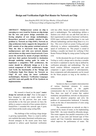
8 7 6 4 3 21 0 Data registers latches the data from data
Length addr byte 0 Header input based on state and status control signals, and
data[0] byte 1 this latched data is sent to the fifo for storage. Apart
data[1] from it, data is also latched into the parity registers
Payload for parity calculation and it is compared with the
parity byte of the packet. An error signal is generated
if packet parity is not equal to the calculated parity
data[N] byte N+1
parity byte N+2 Parity
Data Packet Format
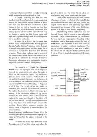
clock
delay
reset
packet_valid
data H D D D P H D D D P
Suspend_data
err
sent packet Packet 1 (addr = 0) Packet 1 (addr =
0)
H = Header, D = Data, P = Parity
Router Input Protocol
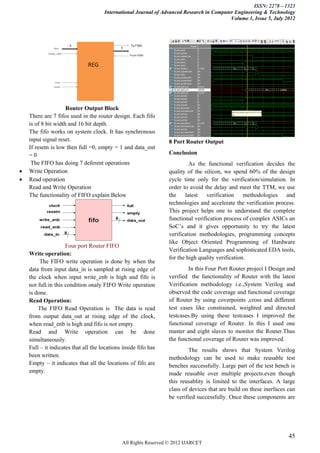
clock
reset
packet_valid
data H D D D P H D D D P
vld_out_0
response delay
read_enb
_0
data_out_0 H D D D P
received
Packet 1 (addr = 0)
packet
Router output Protocol
Register Block:
This module contains status, data and parity
registers required by router. All the registers in this
module are latched on rising edge of the clock.
44
All Rights Reserved © 2012 IJARCET](https://image.slidesharecdn.com/42-46-120812033140-phpapp02/85/42-46-3-320.jpg)


![07 coms 525 tcpip - udp [autosaved]](https://cdn.slidesharecdn.com/ss_thumbnails/07-coms525tcpip-udpautosaved-200102103428-thumbnail.jpg?width=640&height=640&fit=bounds)


![5G Explained! A High Level Overview [Introduction]](https://cdn.slidesharecdn.com/ss_thumbnails/5gexplainedahighleveloverview-260119165306-cc137a3e-thumbnail.jpg?width=640&height=640&fit=bounds)


