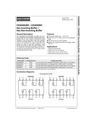
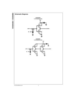
The document summarizes specifications for the CD4049UBC and CD4050BC hex inverting and non-inverting buffer integrated circuits. Key details include:
- They are CMOS devices that can convert logic levels using a single supply voltage.
- Features include a wide supply voltage range of 3-15V and direct driving of 2 TTL loads at 5V.
- Applications include hex inverting/buffer, CMOS to TTL conversion, and current driving.
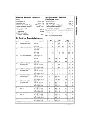
- Electrical characteristics include propagation delay, output current and voltage levels.