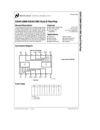
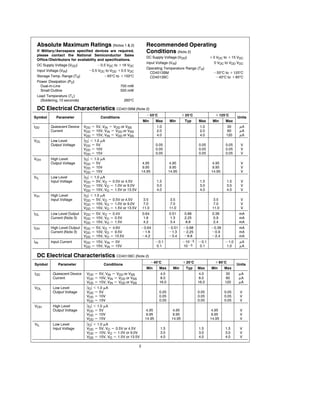
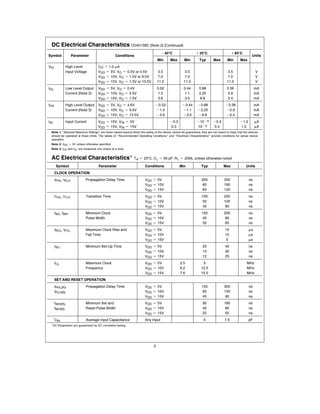
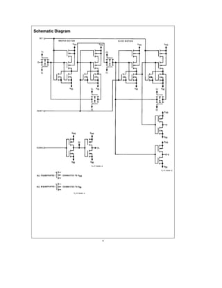
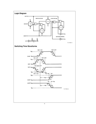
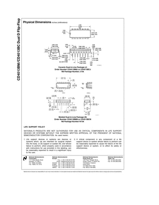
CD4013BM CD4013BC Dual D Flip-Flop
                                                                                                                         February 1988


  CD4013BM CD4013BC Dual D Flip-Flop
  General Description                                                   Features
  The CD4013B dual D flip-flop is a monolithic complementa-             Y   Wide supply voltage range                     3 0V to 15V
  ry MOS (CMOS) integrated circuit constructed with N- and              Y   High noise immunity                        0 45 VDD (typ )
  P-channel enhancement mode transistors Each flip-flop                 Y   Low power TTL                     fan out of 2 driving 74L
  has independent data set reset and clock inputs and ‘‘Q’’                 compatibility                            or 1 driving 74LS
  and ‘‘Q’’ outputs These devices can be used for shift regis-
  ter applications and by connecting ‘‘Q’’ output to the data           Applications
  input for counter and toggle applications The logic level
  present at the ‘‘D’’ input is transferred to the Q output during      Y   Automotive                  Y   Alarm system
  the positive-going transition of the clock pulse Setting or           Y   Data terminals              Y   Industrial electronics
  resetting is independent of the clock and is accomplished             Y   Instrumentation             Y   Remote metering
  by a high level on the set or reset line respectively                 Y   Medical electronics         Y   Computers


  Connection Diagram

                                           Dual-In-Line Package


                                                                                                    Order Number CD4013B


                                                                                TL F 5946 – 1
                                                  Top View


  Truth Table
                                                   CL          D    R       S         Q         Q
                                                   L           0    0       0         0         1
                                                   L           1    0       0         1         0
                                                   K           x    0       0         Q         Q
                                                   x           x    1       0         0         1
                                                   x           x    0       1         1         0
                                                   x           x    1       1         1         1
                                              No change
                                                e Level change
                                              x e Don’t care case


C1995 National Semiconductor Corporation   TL F 5946                                                               RRD-B30M105 Printed in U S A
Absolute Maximum Ratings (Notes 1                       2)         Recommended Operating
  If Military Aerospace specified devices are required               Conditions (Note 2)
  please contact the National Semiconductor Sales
                                                                     DC Supply Voltage (VDD)                      a 3 VDC to a 15 VDC
  Office Distributors for availability and specifications
                                                                     Input Voltage (VIN)                            0 VDC to VDD VDC
  DC Supply Voltage (VDD)             b 0 5 VDC to a 18 VDC
                                                                     Operating Temperature Range (TA)
  Input Voltage (VIN)           b 0 5 VDC to VDD a 0 5 VDC
                                                                       CD4013BM                                     b 55 C to a 125 C
  Storage Temp Range (TS)                 b 65 C to a 150 C            CD4013BC                                      b 40 C to a 85 C
  Power Dissipation (PD)
    Dual-In-Line                                     700 mW
    Small Outline                                    500 mW
  Lead Temperature (TL)
    (Soldering 10 seconds)                             260 C

  DC Electrical Characteristics CD4013BM (Note 2)
                                                                     b 55 C                     a 25 C               a 125 C
Symbol       Parameter                  Conditions                                                                                 Units
                                                                   Min       Max       Min       Typ       Max     Min     Max
IDD      Quiescent Device     VDD e 5V VIN e VDD or VSS                      10                             10               30     mA
         Current              VDD e 10V VIN e VDD or VSS                     20                             20               60     mA
                              VDD e 15V VIN e VDD or VSS                     40                             40              120     mA
VOL      Low Level            lIOl k 1 0 mA
         Output Voltage       VDD e 5V                                       0 05                          0 05            0 05      V
                              VDD e 10V                                      0 05                          0 05            0 05      V
                              VDD e 15V                                      0 05                          0 05            0 05      V
VOH      High Level           lIOl k 1 0 mA
         Output Voltage       VDD e 5V                              4 95               4 95                         4 95             V
                              VDD e 10V                             9 95               9 95                         9 95             V
                              VDD e 15V                            14 95              14 95                        14 95             V
VIL      Low Level            lIOl k 1 0 mA
         Input Voltage        VDD e 5V VO e 0 5V or 4 5V                     15                             15                15     V
                              VDD e 10V VO e 1 0V or 9 0V                    30                             30                30     V
                              VDD e 15V VO e 1 5V or 13 5V                   40                             40                40     V
VIH      High Level           lIOl k 1 0 mA
         Input Voltage        VDD e 5V VO e 0 5V or 4 5V            35                 35                           35               V
                              VDD e 10V VO e 1 0V or 9 0V           70                 70                           70               V
                              VDD e 15V VO e 1 5V or 13 5V         11 0               11 0                         11 0              V
IOL      Low Level Output     VDD e 5V VO e 0 4V                   0 64               0 51       0 88              0 36             mA
         Current (Note 3)     VDD e 10V VO e 0 5V                  16                 13         2 25              09               mA
                              VDD e 15V VO e 1 5V                  42                 34          88               24               mA
IOH      High Level Output    VDD e 5V VO e 4 6V               b 0 64                 b 0 51    b 0 88            b 0 36            mA
         Current (Note 3)     VDD e 10V VO e 9 5V              b1 6                   b1 3      b 2 25            b0 9              mA
                              VDD e 15V VO e 13 5V             b4 2                   b3 4      b8 8              b2 4              mA
IIN      Input Current        VDD e 15V VIN e 0V                             b0 1               b 10 b 5   b0 1            b1 0     mA
                              VDD e 15V VIN e 15V                            01                  10b5       01                10    mA

  DC Electrical Characteristics CD4013BC (Note 2)
                                                                          b 40 C                a 25 C               a 85 C
Symbol        Parameter                   Conditions                                                                               Units
                                                                     Min       Max       Min      Typ      Max     Min     Max
IDD        Quiescent Device    VDD e 5V VIN e VDD or VSS                        40                          40              30      mA
           Current             VDD e 10V VIN e VDD or VSS                       80                          80              60      mA
                               VDD e 15V VIN e VDD or VSS                      16 0                        16 0            120      mA
VOL        Low Level           lIOl k 1 0 mA
           Output Voltage      VDD e 5V                                        0 05                        0 05            0 05     V
                               VDD e 10V                                       0 05                        0 05            0 05     V
                               VDD e 15V                                       0 05                        0 05            0 05     V
VOH        High Level          lIOl k 1 0 mA
           Output Voltage      VDD e 5V                               4 95               4 95                      4 95             V
                               VDD e 10V                              9 95               9 95                      9 95             V
                               VDD e 15V                             14 95              14 95                     14 95             V
VIL        Low Level           lIOl k 1 0 mA
           Input Voltage       VDD e 5V VO e 0 5V or 4 5V                      15                          15              15       V
                               VDD e 10V VO e 1 0V or 9 0V                     30                          30              30       V
                               VDD e 15V VO e 1 5V or 13 5V                    40                          40              40       V

                                                               2
DC Electrical Characteristics CD4013BC (Note 2) (Continued)
                                                                                     b 40 C                    a 25 C                      a 85 C
Symbol             Parameter                       Conditions                                                                                             Units
                                                                                   Min      Max       Min         Typ        Max       Min       Max
VIH            High Level              lIOl k 1 0 mA
               Input Voltage           VDD e 5V VO e 0 5V or 4 5V                  35                 35                               35                     V
                                       VDD e 10V VO e 1 0V or 9 0V                  70                 70                               70                    V
                                       VDD e 15V VO e 1 5V or 13 5V                11 0               11 0                             11 0                   V
IOL            Low Level Output        VDD e 5V VO e 0 4V                          0 52               0 44        0 88                 0 36                  mA
               Current (Note 3)        VDD e 10V VO e 0 5V                          13                 11         2 25                  09                   mA
                                       VDD e 15V VO e 1 5V                          36                 30          88                   24                   mA
IOH            High Level Output       VDD e 5V VO e 4 6V                       b 0 52               b 0 44      b 0 88               b 0 36                 mA
               Current (Note 3)        VDD e 10V VO e 9 5V                      b1 3                 b1 1        b 2 25               b0 9                   mA
                                       VDD e 15V VO e 13 5V                     b3 6                 b3 0        b8 8                 b2 4                   mA
IIN            Input Current           VDD e 15V VIN e 0V                                  b0 3                 b 10 b 5    b0 3                 b1 0        mA
                                       VDD e 15V VIN e 15V                                   03                  10b5        03                   10         mA
  Note 1 ‘‘Absolute Maximum Ratings’’ are those values beyond which the safety of the device cannot be guaranteed they are not meant to imply that the devices
  should be operated at these limits The tables of ‘‘Recommended Operating Conditions’’ and ‘‘Electrical Characteristics’’ provide conditions for actual device
  operation
  Note 2 VSS e 0V unless otherwise specified
  Note 3 IOH and IOL are measured one output at a time


  AC Electrical Characteristics                                 TA e 25 C CL e 50 pF RL e 200k unless otherwise noted

        Symbol                         Parameter                         Conditions                Min             Typ              Max               Units
      CLOCK OPERATION
      tPHL tPLH               Propagation Delay Time                     VDD e 5V                                   200              350                ns
                                                                         VDD e 10V                                   80              160                ns
                                                                         VDD e 15V                                   65              120                ns
      tTHL tTLH               Transition Time                            VDD e 5V                                   100              200                ns
                                                                         VDD e 10V                                   50              100                ns
                                                                         VDD e 15V                                   40               80                ns
      tWL tWH                 Minimum Clock                              VDD e 5V                                   100              200                ns
                              Pulse Width                                VDD e 10V                                   40               80                ns
                                                                         VDD e 15V                                   32               65                ns
      tRCL tFCL               Maximum Clock Rise and                     VDD e 5V                                                     15                ms
                              Fall Time                                  VDD e 10V                                                    10                ms
                                                                         VDD e 15V                                                     5                ms
      tSU                     Minimum Set-Up Time                        VDD e 5V                                   20                40                ns
                                                                         VDD e 10V                                  15                30                ns
                                                                         VDD e 15V                                  12                25                ns
      fCL                     Maximum Clock                              VDD e 5V                  25               5                                  MHz
                              Frequency                                  VDD e 10V                 62              12 5                                MHz
                                                                         VDD e 15V                 76              15 5                                MHz
      SET AND RESET OPERATION
      tPHL(R)                 Propagation Delay Time                     VDD e 5V                                   150              300                ns
      tPLH(S)                                                            VDD e 10V                                   65              130                ns
                                                                         VDD e 15V                                   45               90                ns
      tWH(R)                  Minimum Set and                            VDD e 5V                                   90               180                ns
      tWH(S)                  Reset Pulse Width                          VDD e 10V                                  40                80                ns
                                                                         VDD e 15V                                  25                50                ns
      CIN                     Average Input Capacitance                  Any Input                                   5               75                 pF
      AC Parameters are guaranteed by DC correlated testing


                                                                               3
Schematic Diagram


                                  TL F 5946 – 3

                                                  TL F 5946 – 2


                    TL F 5946–4


                                              4
Logic Diagram


                                        TL F 5946 – 5


Switching Time Waveforms


                               TL F 5946 – 6


                           5
CD4013BM CD4013BC Dual D Flip-Flop
                                     Physical Dimensions inches (millimeters)


                                                                                                              Ceramic Dual-In-Line Package (J)
                                                                                                          Order Number CD4013BMJ or CD4013BCJ
                                                                                                                 NS Package Number J14A


                                                                                                             Molded Dual-In-Line Package (N)
                                                                                                         Order Number CD4013BMN or CD4013BCN
                                                                                                                NS Package Number N14A


                                     LIFE SUPPORT POLICY

                                     NATIONAL’S PRODUCTS ARE NOT AUTHORIZED FOR USE AS CRITICAL COMPONENTS IN LIFE SUPPORT
                                     DEVICES OR SYSTEMS WITHOUT THE EXPRESS WRITTEN APPROVAL OF THE PRESIDENT OF NATIONAL
                                     SEMICONDUCTOR CORPORATION As used herein

                                     1 Life support devices or systems are devices or                                                                 2 A critical component is any component of a life
                                       systems which (a) are intended for surgical implant                                                              support device or system whose failure to perform can
                                       into the body or (b) support or sustain life and whose                                                           be reasonably expected to cause the failure of the life
                                       failure to perform when properly used in accordance                                                              support device or system or to affect its safety or
                                       with instructions for use provided in the labeling can                                                           effectiveness
                                       be reasonably expected to result in a significant injury
                                       to the user

                                                 National Semiconductor                              National Semiconductor                                               National Semiconductor                                  National Semiconductor
                                                 Corporation                                         Europe                                                               Hong Kong Ltd                                           Japan Ltd
                                                 1111 West Bardin Road                                        Fax (a49) 0-180-530 85 86                                   13th Floor Straight Block                               Tel 81-043-299-2309
                                                 Arlington TX 76017                                          Email cnjwge tevm2 nsc com                                   Ocean Centre 5 Canton Rd                                Fax 81-043-299-2408
                                                 Tel 1(800) 272-9959                                 Deutsch Tel (a49) 0-180-530 85 85                                    Tsimshatsui Kowloon
                                                 Fax 1(800) 737-7018                                 English Tel (a49) 0-180-532 78 32                                    Hong Kong
                                                                                                     Fran ais Tel (a49) 0-180-532 93 58                                   Tel (852) 2737-1600
                                                                                                     Italiano Tel (a49) 0-180-534 16 80                                   Fax (852) 2736-9960


                                     National does not assume any responsibility for use of any circuitry described no circuit patent licenses are implied and National reserves the right at any time without notice to change said circuitry and specifications

Cd4013

  • 1.
    CD4013BM CD4013BC DualD Flip-Flop February 1988 CD4013BM CD4013BC Dual D Flip-Flop General Description Features The CD4013B dual D flip-flop is a monolithic complementa- Y Wide supply voltage range 3 0V to 15V ry MOS (CMOS) integrated circuit constructed with N- and Y High noise immunity 0 45 VDD (typ ) P-channel enhancement mode transistors Each flip-flop Y Low power TTL fan out of 2 driving 74L has independent data set reset and clock inputs and ‘‘Q’’ compatibility or 1 driving 74LS and ‘‘Q’’ outputs These devices can be used for shift regis- ter applications and by connecting ‘‘Q’’ output to the data Applications input for counter and toggle applications The logic level present at the ‘‘D’’ input is transferred to the Q output during Y Automotive Y Alarm system the positive-going transition of the clock pulse Setting or Y Data terminals Y Industrial electronics resetting is independent of the clock and is accomplished Y Instrumentation Y Remote metering by a high level on the set or reset line respectively Y Medical electronics Y Computers Connection Diagram Dual-In-Line Package Order Number CD4013B TL F 5946 – 1 Top View Truth Table CL D R S Q Q L 0 0 0 0 1 L 1 0 0 1 0 K x 0 0 Q Q x x 1 0 0 1 x x 0 1 1 0 x x 1 1 1 1 No change e Level change x e Don’t care case C1995 National Semiconductor Corporation TL F 5946 RRD-B30M105 Printed in U S A
  • 2.
    Absolute Maximum Ratings(Notes 1 2) Recommended Operating If Military Aerospace specified devices are required Conditions (Note 2) please contact the National Semiconductor Sales DC Supply Voltage (VDD) a 3 VDC to a 15 VDC Office Distributors for availability and specifications Input Voltage (VIN) 0 VDC to VDD VDC DC Supply Voltage (VDD) b 0 5 VDC to a 18 VDC Operating Temperature Range (TA) Input Voltage (VIN) b 0 5 VDC to VDD a 0 5 VDC CD4013BM b 55 C to a 125 C Storage Temp Range (TS) b 65 C to a 150 C CD4013BC b 40 C to a 85 C Power Dissipation (PD) Dual-In-Line 700 mW Small Outline 500 mW Lead Temperature (TL) (Soldering 10 seconds) 260 C DC Electrical Characteristics CD4013BM (Note 2) b 55 C a 25 C a 125 C Symbol Parameter Conditions Units Min Max Min Typ Max Min Max IDD Quiescent Device VDD e 5V VIN e VDD or VSS 10 10 30 mA Current VDD e 10V VIN e VDD or VSS 20 20 60 mA VDD e 15V VIN e VDD or VSS 40 40 120 mA VOL Low Level lIOl k 1 0 mA Output Voltage VDD e 5V 0 05 0 05 0 05 V VDD e 10V 0 05 0 05 0 05 V VDD e 15V 0 05 0 05 0 05 V VOH High Level lIOl k 1 0 mA Output Voltage VDD e 5V 4 95 4 95 4 95 V VDD e 10V 9 95 9 95 9 95 V VDD e 15V 14 95 14 95 14 95 V VIL Low Level lIOl k 1 0 mA Input Voltage VDD e 5V VO e 0 5V or 4 5V 15 15 15 V VDD e 10V VO e 1 0V or 9 0V 30 30 30 V VDD e 15V VO e 1 5V or 13 5V 40 40 40 V VIH High Level lIOl k 1 0 mA Input Voltage VDD e 5V VO e 0 5V or 4 5V 35 35 35 V VDD e 10V VO e 1 0V or 9 0V 70 70 70 V VDD e 15V VO e 1 5V or 13 5V 11 0 11 0 11 0 V IOL Low Level Output VDD e 5V VO e 0 4V 0 64 0 51 0 88 0 36 mA Current (Note 3) VDD e 10V VO e 0 5V 16 13 2 25 09 mA VDD e 15V VO e 1 5V 42 34 88 24 mA IOH High Level Output VDD e 5V VO e 4 6V b 0 64 b 0 51 b 0 88 b 0 36 mA Current (Note 3) VDD e 10V VO e 9 5V b1 6 b1 3 b 2 25 b0 9 mA VDD e 15V VO e 13 5V b4 2 b3 4 b8 8 b2 4 mA IIN Input Current VDD e 15V VIN e 0V b0 1 b 10 b 5 b0 1 b1 0 mA VDD e 15V VIN e 15V 01 10b5 01 10 mA DC Electrical Characteristics CD4013BC (Note 2) b 40 C a 25 C a 85 C Symbol Parameter Conditions Units Min Max Min Typ Max Min Max IDD Quiescent Device VDD e 5V VIN e VDD or VSS 40 40 30 mA Current VDD e 10V VIN e VDD or VSS 80 80 60 mA VDD e 15V VIN e VDD or VSS 16 0 16 0 120 mA VOL Low Level lIOl k 1 0 mA Output Voltage VDD e 5V 0 05 0 05 0 05 V VDD e 10V 0 05 0 05 0 05 V VDD e 15V 0 05 0 05 0 05 V VOH High Level lIOl k 1 0 mA Output Voltage VDD e 5V 4 95 4 95 4 95 V VDD e 10V 9 95 9 95 9 95 V VDD e 15V 14 95 14 95 14 95 V VIL Low Level lIOl k 1 0 mA Input Voltage VDD e 5V VO e 0 5V or 4 5V 15 15 15 V VDD e 10V VO e 1 0V or 9 0V 30 30 30 V VDD e 15V VO e 1 5V or 13 5V 40 40 40 V 2
  • 3.
    DC Electrical CharacteristicsCD4013BC (Note 2) (Continued) b 40 C a 25 C a 85 C Symbol Parameter Conditions Units Min Max Min Typ Max Min Max VIH High Level lIOl k 1 0 mA Input Voltage VDD e 5V VO e 0 5V or 4 5V 35 35 35 V VDD e 10V VO e 1 0V or 9 0V 70 70 70 V VDD e 15V VO e 1 5V or 13 5V 11 0 11 0 11 0 V IOL Low Level Output VDD e 5V VO e 0 4V 0 52 0 44 0 88 0 36 mA Current (Note 3) VDD e 10V VO e 0 5V 13 11 2 25 09 mA VDD e 15V VO e 1 5V 36 30 88 24 mA IOH High Level Output VDD e 5V VO e 4 6V b 0 52 b 0 44 b 0 88 b 0 36 mA Current (Note 3) VDD e 10V VO e 9 5V b1 3 b1 1 b 2 25 b0 9 mA VDD e 15V VO e 13 5V b3 6 b3 0 b8 8 b2 4 mA IIN Input Current VDD e 15V VIN e 0V b0 3 b 10 b 5 b0 3 b1 0 mA VDD e 15V VIN e 15V 03 10b5 03 10 mA Note 1 ‘‘Absolute Maximum Ratings’’ are those values beyond which the safety of the device cannot be guaranteed they are not meant to imply that the devices should be operated at these limits The tables of ‘‘Recommended Operating Conditions’’ and ‘‘Electrical Characteristics’’ provide conditions for actual device operation Note 2 VSS e 0V unless otherwise specified Note 3 IOH and IOL are measured one output at a time AC Electrical Characteristics TA e 25 C CL e 50 pF RL e 200k unless otherwise noted Symbol Parameter Conditions Min Typ Max Units CLOCK OPERATION tPHL tPLH Propagation Delay Time VDD e 5V 200 350 ns VDD e 10V 80 160 ns VDD e 15V 65 120 ns tTHL tTLH Transition Time VDD e 5V 100 200 ns VDD e 10V 50 100 ns VDD e 15V 40 80 ns tWL tWH Minimum Clock VDD e 5V 100 200 ns Pulse Width VDD e 10V 40 80 ns VDD e 15V 32 65 ns tRCL tFCL Maximum Clock Rise and VDD e 5V 15 ms Fall Time VDD e 10V 10 ms VDD e 15V 5 ms tSU Minimum Set-Up Time VDD e 5V 20 40 ns VDD e 10V 15 30 ns VDD e 15V 12 25 ns fCL Maximum Clock VDD e 5V 25 5 MHz Frequency VDD e 10V 62 12 5 MHz VDD e 15V 76 15 5 MHz SET AND RESET OPERATION tPHL(R) Propagation Delay Time VDD e 5V 150 300 ns tPLH(S) VDD e 10V 65 130 ns VDD e 15V 45 90 ns tWH(R) Minimum Set and VDD e 5V 90 180 ns tWH(S) Reset Pulse Width VDD e 10V 40 80 ns VDD e 15V 25 50 ns CIN Average Input Capacitance Any Input 5 75 pF AC Parameters are guaranteed by DC correlated testing 3
  • 4.
    Schematic Diagram TL F 5946 – 3 TL F 5946 – 2 TL F 5946–4 4
  • 5.
    Logic Diagram TL F 5946 – 5 Switching Time Waveforms TL F 5946 – 6 5
  • 6.
    CD4013BM CD4013BC DualD Flip-Flop Physical Dimensions inches (millimeters) Ceramic Dual-In-Line Package (J) Order Number CD4013BMJ or CD4013BCJ NS Package Number J14A Molded Dual-In-Line Package (N) Order Number CD4013BMN or CD4013BCN NS Package Number N14A LIFE SUPPORT POLICY NATIONAL’S PRODUCTS ARE NOT AUTHORIZED FOR USE AS CRITICAL COMPONENTS IN LIFE SUPPORT DEVICES OR SYSTEMS WITHOUT THE EXPRESS WRITTEN APPROVAL OF THE PRESIDENT OF NATIONAL SEMICONDUCTOR CORPORATION As used herein 1 Life support devices or systems are devices or 2 A critical component is any component of a life systems which (a) are intended for surgical implant support device or system whose failure to perform can into the body or (b) support or sustain life and whose be reasonably expected to cause the failure of the life failure to perform when properly used in accordance support device or system or to affect its safety or with instructions for use provided in the labeling can effectiveness be reasonably expected to result in a significant injury to the user National Semiconductor National Semiconductor National Semiconductor National Semiconductor Corporation Europe Hong Kong Ltd Japan Ltd 1111 West Bardin Road Fax (a49) 0-180-530 85 86 13th Floor Straight Block Tel 81-043-299-2309 Arlington TX 76017 Email cnjwge tevm2 nsc com Ocean Centre 5 Canton Rd Fax 81-043-299-2408 Tel 1(800) 272-9959 Deutsch Tel (a49) 0-180-530 85 85 Tsimshatsui Kowloon Fax 1(800) 737-7018 English Tel (a49) 0-180-532 78 32 Hong Kong Fran ais Tel (a49) 0-180-532 93 58 Tel (852) 2737-1600 Italiano Tel (a49) 0-180-534 16 80 Fax (852) 2736-9960 National does not assume any responsibility for use of any circuitry described no circuit patent licenses are implied and National reserves the right at any time without notice to change said circuitry and specifications