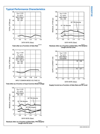
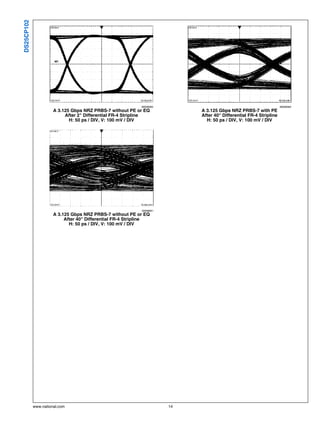
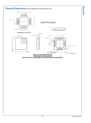
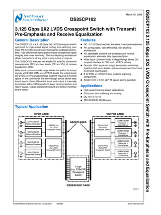
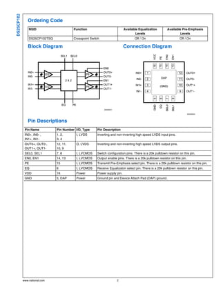
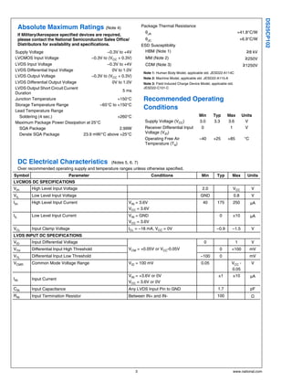
The DS25CP102 is a 3.125 Gbps 2x2 LVDS crosspoint switch that can route signals between inputs and outputs. It features transmit pre-emphasis and receive equalization to eliminate data-dependent jitter. The small package size minimizes space on circuit boards. Applications include high-speed channel selection, clock and data buffering/multiplexing, and SD/HD/3D video routing.
The document describes the LM6171 high speed low power low distortion voltage feedback amplifier. Key features include:
- Unity-gain bandwidth of 100 MHz and slew rate of 3600V/μs while consuming only 2.5 mA of supply current.
- Specified for operation with supply voltages of ±15V and ±5V.
- Built on National's advanced VIPTM III complementary bipolar process.
- Suitable for applications such as video amplifiers, line drivers, ADC/DAC buffers, and instrumentation amplifiers.
The document provides information about the PDIUSBD11 USB peripheral chip from Philips Semiconductor, including its features, specifications, pin descriptions, example schematic, and considerations for bus and self-powered operation. It summarizes that the chip allows microcontrollers a USB interface using various transfer modes at full USB speed. However, its documentation and software support are lacking, making initialization difficult without additional information.
The document summarizes the 74LCX08 low voltage quad 2-input AND gate. It contains four 2-input AND gates with 5V tolerant inputs that can interface 5V systems to 3V systems. It is fabricated with advanced CMOS technology to achieve high speed operation while maintaining low power dissipation. Key features include 5V tolerant inputs, 2.3V-3.6V power supply specifications, 5.5ns max propagation delay, 10uA max supply current, and ESD and latch-up performance.
This document is a datasheet for the TD1410, a 380KHz fixed frequency monolithic step down switch mode regulator with a built in internal Power MOSFET capable of delivering 2A of continuous output current over a wide input voltage range. The datasheet provides details on the device including electrical specifications, typical application circuits, thermal considerations, and function descriptions of the various pins. It is intended to provide engineers with the necessary information to properly utilize the TD1410 in their circuit designs.
The UTC 4051 is an 8-channel analog multiplexer/demultiplexer chip that allows for digitally controlled switching of analog signals. It has three binary control inputs, an inhibit input, and features low on impedance and very low off leakage current. The chip supports analog signal switching across a wide voltage range of 3V to 18V.
The document describes the AD7524, an 8-bit CMOS DAC designed for direct interface with microprocessors. It provides key specifications such as 8-bit resolution, accuracy of ±1/2 LSB typical, low power consumption under 10mW, and compatibility with common microprocessor buses and ports. The AD7524 is suitable for applications including microprocessor controlled gain circuits, attenuators, function generation, and precision automatic gain control circuits.
This document provides a macromodel for the MC33078 dual operational amplifier. The macromodel code is provided which models the input stage, amplifying stage, and output stage of the operational amplifier. Electrical characteristics obtained from simulations using the macromodel are also listed, including voltage gain, supply current, input common mode voltage range, and other key parameters.
1. The document describes the VIPer22A, a low power offline SMPS primary switcher integrated circuit that combines a current mode PWM controller with a high voltage power MOSFET.
2. The VIPer22A has a wide input voltage range of 85-265V, output power capabilities of 7-20W, and a fixed switching frequency of 60kHz.
3. It features current mode control, undervoltage lockout, overtemperature protection, and can accommodate supply voltages from 9-38V on its VDD pin.
Delta Electronics adds two Redundancy Modules, DRR-20A and DRR-40A to its
CliQ II series of DIN Rail power management products. They are compatible with
both 24Vdc and 48Vdc power supplies, offering redundancy functionality. These
modules can also be used for Parallel operation.
The document discusses offline power supply configurations and new products from Electronicos Online. It introduces the VIPer+ family of controllers for power supplies with adjustable current limiting and protections. The VIPer+ offers improved technology over previous controllers with an 800V power MOSFET. It provides functionalities like soft start, burst mode, and adjustable current limiting set points. Protections include overvoltage, overcurrent, overtemperature and more. A roadmap shows the expanding portfolio of HV converter products from 1W to 50W.
The μA741 is a general-purpose operational amplifier featuring offset-voltage null capability. It has a high common-mode input voltage range, short-circuit protection, and stability without external components. The μA741 is available in various package options and is characterized for operation over different temperature ranges depending on the specific part number.
The LM124/SA534/LM2902 series consists of four independent, high-gain, internally frequency-compensated operational amplifiers designed specifically to operate from a single power supply over a wide range of voltages.
The document describes a multiple output power supply design for a DVD player with the following key points:
1. It provides 7.5W of continuous output power and 13W of peak power with outputs of 3.3V, 5V, 12V, and -12V regulated using a TinySwitch-PK controller in a flyback topology.
2. It achieves good cross-regulation between the 5V and 3.3V outputs through minimizing leakage and sum regulating the feedback.
3. It includes features for EMI filtering, surge protection, clamping, and a unique peak mode for boosting current limit during peaks loads.
Sepam series 40 is a family of digital protection relays used for current and voltage protection in medium and low voltage distribution systems. It includes 7 base unit types for substation, transformer, motor, and generator protection. The base units have various interfaces and can accept optional input/output modules. The relays perform protections like overcurrent, earth fault, over/under voltage, and thermal overload. They also provide metering, diagnostics, control, and communication functions.
The document provides product descriptions for various components of the RPS (Remote Power Supply) system, including:
1) The central office (CO) unit which enables power transfer of up to 100W via twisted pair channels at a source voltage of ±190V.
2) Remote power (RP) units like the MRODx shelf that houses DC/DC converters and control units to provide up to 900W of output power.
3) DC/DC converter modules like the PDL that combine three converters to supply 45-75W per twisted pair at input voltages from 230-380V.
This document provides information on the LPC662 low power CMOS dual operational amplifier:
- It is ideal for single supply operation from +5V to +15V with rail-to-rail output swing and input common-mode range including ground.
- Key features include micropower operation (<0.5mW), high voltage gain (120dB), low input offset voltage (3mV), and ultra low input bias current (2fA).
- Applications include high-impedance buffer, precision current-to-voltage converter, long-term integrator, high-impedance preamplifier, active filter, sample-and-hold circuit, and peak detector.
The document describes a 20mA LED driver demo board that operates from 10-400V DC or 10-265V AC input and can power a single 20mA LED or string of LEDs up to 9V. The circuit uses an HV9821 control IC to operate in three modes - clamped buck converter, buck converter, or resistive ballast - depending on the line and load conditions. The board is designed to meet EMI standards and provides LED current regulation within 3% over the input voltage range while consuming less than 1W of power.
The document summarizes specifications for the CD4049UBC and CD4050BC hex inverting and non-inverting buffer integrated circuits. Key details include:
- They are CMOS devices that can convert logic levels using a single supply voltage.
- Features include a wide supply voltage range of 3-15V and direct driving of 2 TTL loads at 5V.
- Applications include hex inverting/buffer, CMOS to TTL conversion, and current driving.
- Electrical characteristics include propagation delay, output current and voltage levels.
1. Betagard 5SX4 miniature circuit breakers (MCBs) have rated breaking capacities up to 10kA and comply with national and international standards with current ratings from 0.5A to 63A.
2. 5SX4 MCBs significantly limit let-through current during faults, providing high protection. They have "C" and "D" tripping characteristics and an average service life of 20,000 operations.
3. 5SX4 MCBs provide selectivity (preventing unnecessary tripping of upstream devices) when used with fuses or other MCBs according to limits specified in the document.
The document describes a BO-X2-SFP+ X2 converter that allows the use of an SFP+ module in an X2 port. It has an XAUI electrical interface and is compliant with various industry standards. The converter provides real-time diagnostic information on operating conditions through its digital interface.
This document summarizes the MiniDySC 12 Amps voltage sag corrector from SoftSwitching Technologies. It is designed to protect sensitive electronic components from short-term voltage sags, keeping equipment online and productivity levels high. It features a proprietary double conversion power core, the fastest sag detection and response time on the market of 1 ms, and true sinusoidal reconstruction of the output waveform. It has a standard runtime of 21.1 inches, can correct voltages from 100-240V, and provides 1.2-3 kVA of output capacity to protect components.
This document provides guidance on reading electrical specification datasheets. It explains that datasheets contain important maximum, minimum, and typical ratings for components under various test conditions. Key sections are identified, such as DC characteristics that specify voltage and current levels, and AC characteristics that define timing parameters. The document stresses the need to carefully consider test conditions and understand how component performance may vary with operating conditions like temperature, voltage, and load. Overall, the document aims to educate engineers on extracting critical design constraints from datasheet specifications.
The document provides a diagram and description of a photovoltaic solar array system. The system includes 8 solar panels that feed power into an inverter which converts the DC power to 240V AC power. It then connects to the main electrical service panel of a home and includes disconnect switches, grounding conductors, and a bi-directional utility meter to allow excess power to be sold back to the electric company. Safety notes and equipment listings are also included.
The document provides technical information about the TA2021B, a 25W per channel Class-T digital audio power amplifier integrated circuit from Tripath Technology. Some key details include:
- It uses Tripath's proprietary Digital Power Processing (DPPTM) technology for high efficiency amplification with audiophile quality sound.
- It can provide up to 25W of continuous power per channel into a 4 ohm load, with over 80% efficiency and very low distortion.
- It has a wide dynamic range of 100dB and interfaces designed for use in applications like DVD receivers, PC multimedia systems, and more.
- Electrical characteristics, operating conditions, pin descriptions and other specifications are provided to help
The document provides information on Siemens 3TH30 contactor relays:
1) 3TH30 contactor relays are air break contactors suitable for 10A at 240V AC and 10A at 24V DC that provide reliability and safety in control circuits.
2) They have flexible configurations with up to 8 contacts and mounting options.
3) Features include double break parallel bridge contacts, captive screws, and lugless terminations for improved safety and ease of use.
The document summarizes the PCA9532, a 16-bit I2C LED dimmer chip. It contains 16 LED drivers that can individually set the LEDs to on, off, or one of two programmable blinking rates. The blinking rates and duty cycles can be programmed to provide 256 brightness steps. The chip contains internal oscillators and PWM circuitry to generate the blinking without external components. It can directly drive LEDs with up to 25mA of current per pin.
This document provides specifications for an SFP-1G-CWDM-1290-80-T02 1G CWDM SFP transceiver module that operates at 1290nm wavelength over 80km of single mode fiber. Key features include a 1.25Gbps data rate, LC duplex connector, hot pluggable SFP form factor, low power consumption under 0.8W, and operating temperature range of 0-70°C. The document includes detailed optical and electrical parameters and pinouts.
This document describes a dual 12-bit DAC chip. It contains two 12-bit DACs, on-chip voltage reference, output amplifiers, and reference buffer amplifiers. It can operate from a single or dual power supply. Key specifications include 12-bit resolution, differential nonlinearity of ±0.9 LSB max, output ranges of 0-5V, 0-10V, and ±5V. The chip comes in a 28-lead CQFP package and is screened using various reliability tests according to MIL-STD-883.
This document provides specifications for a 1G 1610nm 80km CWDM SFP transceiver module. Key details include:
- It operates at 1.25Gbps up to 80km on single mode fiber with a 1610nm CWDM laser transmitter.
- Electrical characteristics include a supply voltage of 3.13-3.47V and supply current of up to 220mA.
- Optical characteristics include an average output power of 0-5dBm and receiver sensitivity of -24dBm.
- It has digital diagnostic monitoring interfaces and complies with SFP MSA standards.
This document provides specifications for a 1G 1590nm 80km CWDM SFP transceiver module. Key details include:
- It operates at 1.25Gbps up to 80km on single mode fiber with a 1590nm CWDM laser transmitter.
- Electrical characteristics include a supply voltage of 3.13-3.47V and supply current below 220mA.
- Optical characteristics include an average output power of 0-5dBm and receiver sensitivity down to -24dBm.
- It has hot pluggable SFP form factor and complies with relevant SFP MSA standards.
This document describes a 1G 1370nm 80km CWDM SFP transceiver module. It provides specifications for the optical and electrical characteristics including operating wavelength of 1370nm, transmission distance of 80km, data rate of 1.25Gbps, operating temperature range of 0-70°C, and compliance with SFP MSA standards. Diagrams and details are given for the functional blocks, pin definitions and interface.
This document provides specifications for a 1G 1270nm 80km CWDM SFP transceiver module. It includes details on the product description, features, functional diagram, electrical and optical characteristics, pin definitions, digital diagnostic specifications, typical interface circuit, package dimensions, and ordering information. The module uses a CWDM DFB laser transmitter, PIN photodiode receiver, and MCU control to support data transmission up to 1.25Gbps over 80km of single mode fiber.
This document provides specifications for a 1G 1490nm 80km CWDM SFP transceiver module. It includes details on the product description, features, application, functional diagram, electrical and optical characteristics, pin definitions, digital diagnostic specifications, typical interface circuit, package dimensions, and ordering information. The module uses a 1490nm CWDM DFB laser transmitter, PIN photodiode receiver, and MCU control to support data rates up to 1.25Gbps and transmission distances of 80km on single mode fiber.
This document describes a 1G 1570nm 80km CWDM SFP transceiver module. It provides specifications for the optical and electrical characteristics including a wavelength of 1570nm, transmission distance of 80km, data rate of 1.25Gbps, and operating case temperature range of 0-70°C. Also included are the functional diagram, pin definitions, digital diagnostic specifications, package dimensions, and ordering information.
This document provides specifications for a 1G 1510nm 80km CWDM SFP transceiver module. It includes details on the product description, features, application, functional diagram, electrical and optical characteristics, pin definitions, digital diagnostic specifications, typical interface circuit, package dimensions, and ordering information. The module uses a CWDM DFB laser transmitter, PIN photodiode receiver, and MCU control to support data rates up to 1.25Gbps and transmission distances of 80km on single mode fiber.
This document describes a 1G 1390nm 80km CWDM SFP transceiver. It operates at 1.25Gbps up to 80km on single mode fiber. The transceiver uses a 1390nm CWDM DFB laser transmitter and PIN photodiode receiver. It complies with SFP MSA standards and supports digital diagnostic monitoring interfaces. Specifications for optical and electrical performance, operating conditions, pin definitions and mechanical dimensions are provided.
This document provides specifications for a 1G 1410nm 80km CWDM SFP transceiver module. The module uses a 1410nm laser transmitter and photo detector to transmit data up to 1.25Gbps over 80km of single mode fiber. It has an operating temperature range of 0-70°C and complies with SFP MSA standards. Key parameters including optical power, wavelength, rise/fall time, and receiver sensitivity are specified.
This document provides specifications for a 1G 1550nm 80km CWDM SFP transceiver. It operates at 1.25Gbps up to 80km on single mode fiber. The transceiver uses an uncooled CWDM laser transmitter, photodiode receiver, and MCU control unit. It complies with SFP MSA standards and supports gigabit Ethernet, WDM systems, and other optical transmission applications. Electrical, optical, mechanical and diagnostic specifications are provided to characterize the performance and interface of the transceiver.
This document provides specifications for a 1G 1430nm 80km CWDM SFP transceiver. It includes details on the product description, features, application, functional diagram, electrical and optical characteristics, pin definitions, digital diagnostic specifications, typical interface circuit, package dimensions, and ordering information. The transceiver uses a 1430nm CWDM laser transmitter and photo detector with a transmission distance of 80km on SMF fiber. It supports 1.25Gbps data rates and is compliant with SFP MSA standards.
This document describes the specifications of an SFP-1G-CWDM-1470-80 transceiver module. The module operates at a wavelength of 1470nm, supports data rates up to 1.25Gbps, and can transmit over single mode fiber for distances up to 80km. The document provides detailed information on the module's optical and electrical characteristics, functional diagram, pin definitions, and ordering part numbers.
This document provides specifications for a 1G 1350nm 80km CWDM SFP transceiver module. Key details include:
- It operates at 1.25Gbps up to 80km on single mode fiber with a 1350nm CWDM laser transmitter.
- Features include an integrated laser, photodiode, TIA and control unit with LC connectors and hot pluggable SFP form factor.
- Optical and electrical specifications are provided for the transmitter and receiver including wavelength, power levels, data rates and temperature ranges.
- Pinouts and interface diagrams are shown along with digital diagnostic monitoring capabilities.
1) The document describes a 1G 1530nm 80km CWDM SFP transceiver module that operates at 1.25Gbps and can transmit over 80km of single mode fiber.
2) The module contains a CWDM DFB laser transmitter, photodiode receiver, and MCU control unit. It supports hot-pluggable SFP form factor and complies with relevant standards.
3) Key features include a 1530nm laser wavelength, 80km transmission distance, low power consumption, digital diagnostic monitoring interface, and operating temperature range of 0-70°C.
This document describes a 1.25Gbps SFP transceiver module that transmits at 1550nm and receives at 1310nm with a transmission distance of 10km. It consists of a DFB laser transmitter, photodiode receiver, and MCU control unit. The module operates at dual data rates of 1.25Gbps/1.063Gbps and has applications in Ethernet, Fibre Channel, and other optical transmission systems. It complies with various industry standards and has an operating temperature range of 0-70°C or -40-85°C depending on the model.
This document provides specifications for the SFP-1G-CWDM-1450-80-T02 1G 1450nm 80km CWDM SFP transceiver module. The module supports data rates up to 1.25Gbps and transmission over 80km of single mode fiber. It consists of an uncooled CWDM laser transmitter, photodiode receiver, and MCU control unit. Key specifications include an operating wavelength of 1450nm, average output power between 0-5dBm, receiver sensitivity down to -24dBm, and operating temperature range of 0-70°C.
The Microchip Technology Inc. MCP3201 device is a 12-bit analog-to-digital converter with an on-board sample and hold circuit. It has a single input and communicates using a serial interface compatible with SPI. It can sample at up to 100 ksps at 5V or 50 ksps at 2.7V. It has low power consumption and operates over a voltage range of 2.7-5.5V. It is available in 8-pin MSOP, PDIP, SOIC, and TSSOP packages.
Update 22 models(Schottky Rectifier ) in SPICE PARK(APR2024)Tsuyoshi Horigome
This document provides an inventory update of 6,747 parts at Spice Park as of April 2024. It lists the part numbers, manufacturers, and quantities of various semiconductor components, including 1,697 Schottky rectifier diodes from 29 different manufacturers. It also includes details on passive components, batteries, mechanical parts, motors, and lamps in the inventory.
The document provides an inventory update from April 2024 of the Spice Park collection which contains 6,747 electronic components. It includes tables listing the types of semiconductor components, passive parts, batteries, mechanical parts, motors, and lamps in the collection along with their manufacturer and quantities. One of the semiconductor components, the general purpose rectifier diode, is broken down into a more detailed table with 116 entries providing part numbers, manufacturers, thermal ratings, and remarks.
Update 31 models(Diode/General ) in SPICE PARK(MAR2024)Tsuyoshi Horigome
The document provides an inventory update from March 2024 of parts in the Spice Park warehouse. It lists 6,725 total parts across various categories including semiconductors, passive parts, batteries, mechanical parts, motors, and lamps. The semiconductor section lists 652 general purpose rectifier diodes from 18 different manufacturers with quantities ranging from 2 to 145 pieces.
This document provides an inventory list of parts at Spice Park as of March 2024. It contains 3 sections - Semiconductor parts (diodes, transistors, ICs etc.), Passive parts (capacitors, resistors etc.), and Battery parts. For Semiconductor parts, it lists 36 different part types and provides the quantity of each part. It then provides further details of Diode/General Purpose Rectifiers, listing the manufacturer and quantity of 652 individual part numbers.
Update 29 models(Solar cell) in SPICE PARK(FEB2024)Tsuyoshi Horigome
The document provides an inventory update from February 2024 of Spice Park, which contains 6,694 total pieces of electronic components and parts. It lists 36 categories of semiconductor devices, 11 categories of passive parts, 10 types of batteries, 5 mechanical parts, DC motors, lamps, and power supplies. It provides the most detailed listing for solar cells, with 1,003 total pieces from 51 manufacturers listed with part numbers.
The document provides an inventory update from February 2024 of Spice Park, which contains 6,694 electronic components. It lists the components by type (e.g. semiconductor), part number, manufacturer, thermal rating, and quantity on hand. For example, it shows that there are 621 general purpose rectifier diodes from manufacturers such as Fairchild, Fuji, Intersil, Rohm, Shindengen, and Toshiba. The detailed four-page section provides further information on the first item, general purpose rectifier diodes, including 152 individual part numbers and specifications.
This document discusses circuit simulations using LTspice. It describes driving a circuit simulation by inserting a 250 ohm resistor between the output terminals. It also describes simulating a 1 channel bridge circuit where the DUT1 and DUT2 resistors are both set to 100 ohms and the input voltage is set to either 1V or 5V.
This document discusses parametric sweeps of external and internal resistance values Rg for circuit simulation in LTspice. It also references outputting a waveform similar to a report on fall time characteristics for a device modeling report with customer Samsung.
GraphSummit Singapore | The Future of Agility: Supercharging Digital Transfor...Neo4j
Leonard Jayamohan, Partner & Generative AI Lead, Deloitte
This keynote will reveal how Deloitte leverages Neo4j’s graph power for groundbreaking digital twin solutions, achieving a staggering 100x performance boost. Discover the essential role knowledge graphs play in successful generative AI implementations. Plus, get an exclusive look at an innovative Neo4j + Generative AI solution Deloitte is developing in-house.
In his public lecture, Christian Timmerer provides insights into the fascinating history of video streaming, starting from its humble beginnings before YouTube to the groundbreaking technologies that now dominate platforms like Netflix and ORF ON. Timmerer also presents provocative contributions of his own that have significantly influenced the industry. He concludes by looking at future challenges and invites the audience to join in a discussion.
In the rapidly evolving landscape of technologies, XML continues to play a vital role in structuring, storing, and transporting data across diverse systems. The recent advancements in artificial intelligence (AI) present new methodologies for enhancing XML development workflows, introducing efficiency, automation, and intelligent capabilities. This presentation will outline the scope and perspective of utilizing AI in XML development. The potential benefits and the possible pitfalls will be highlighted, providing a balanced view of the subject.
We will explore the capabilities of AI in understanding XML markup languages and autonomously creating structured XML content. Additionally, we will examine the capacity of AI to enrich plain text with appropriate XML markup. Practical examples and methodological guidelines will be provided to elucidate how AI can be effectively prompted to interpret and generate accurate XML markup.
Further emphasis will be placed on the role of AI in developing XSLT, or schemas such as XSD and Schematron. We will address the techniques and strategies adopted to create prompts for generating code, explaining code, or refactoring the code, and the results achieved.
The discussion will extend to how AI can be used to transform XML content. In particular, the focus will be on the use of AI XPath extension functions in XSLT, Schematron, Schematron Quick Fixes, or for XML content refactoring.
The presentation aims to deliver a comprehensive overview of AI usage in XML development, providing attendees with the necessary knowledge to make informed decisions. Whether you’re at the early stages of adopting AI or considering integrating it in advanced XML development, this presentation will cover all levels of expertise.
By highlighting the potential advantages and challenges of integrating AI with XML development tools and languages, the presentation seeks to inspire thoughtful conversation around the future of XML development. We’ll not only delve into the technical aspects of AI-powered XML development but also discuss practical implications and possible future directions.
Goodbye Windows 11: Make Way for Nitrux Linux 3.5.0!SOFTTECHHUB
As the digital landscape continually evolves, operating systems play a critical role in shaping user experiences and productivity. The launch of Nitrux Linux 3.5.0 marks a significant milestone, offering a robust alternative to traditional systems such as Windows 11. This article delves into the essence of Nitrux Linux 3.5.0, exploring its unique features, advantages, and how it stands as a compelling choice for both casual users and tech enthusiasts.
Sudheer Mechineni, Head of Application Frameworks, Standard Chartered Bank
Discover how Standard Chartered Bank harnessed the power of Neo4j to transform complex data access challenges into a dynamic, scalable graph database solution. This keynote will cover their journey from initial adoption to deploying a fully automated, enterprise-grade causal cluster, highlighting key strategies for modelling organisational changes and ensuring robust disaster recovery. Learn how these innovations have not only enhanced Standard Chartered Bank’s data infrastructure but also positioned them as pioneers in the banking sector’s adoption of graph technology.
UiPath Test Automation using UiPath Test Suite series, part 5DianaGray10
Welcome to UiPath Test Automation using UiPath Test Suite series part 5. In this session, we will cover CI/CD with devops.
Topics covered:
CI/CD with in UiPath
End-to-end overview of CI/CD pipeline with Azure devops
Speaker:
Lyndsey Byblow, Test Suite Sales Engineer @ UiPath, Inc.
Climate Impact of Software Testing at Nordic Testing DaysKari Kakkonen
My slides at Nordic Testing Days 6.6.2024
Climate impact / sustainability of software testing discussed on the talk. ICT and testing must carry their part of global responsibility to help with the climat warming. We can minimize the carbon footprint but we can also have a carbon handprint, a positive impact on the climate. Quality characteristics can be added with sustainability, and then measured continuously. Test environments can be used less, and in smaller scale and on demand. Test techniques can be used in optimizing or minimizing number of tests. Test automation can be used to speed up testing.
Building Production Ready Search Pipelines with Spark and MilvusZilliz
Spark is the widely used ETL tool for processing, indexing and ingesting data to serving stack for search. Milvus is the production-ready open-source vector database. In this talk we will show how to use Spark to process unstructured data to extract vector representations, and push the vectors to Milvus vector database for search serving.
Unlock the Future of Search with MongoDB Atlas_ Vector Search Unleashed.pdfMalak Abu Hammad
Discover how MongoDB Atlas and vector search technology can revolutionize your application's search capabilities. This comprehensive presentation covers:
* What is Vector Search?
* Importance and benefits of vector search
* Practical use cases across various industries
* Step-by-step implementation guide
* Live demos with code snippets
* Enhancing LLM capabilities with vector search
* Best practices and optimization strategies
Perfect for developers, AI enthusiasts, and tech leaders. Learn how to leverage MongoDB Atlas to deliver highly relevant, context-aware search results, transforming your data retrieval process. Stay ahead in tech innovation and maximize the potential of your applications.
#MongoDB #VectorSearch #AI #SemanticSearch #TechInnovation #DataScience #LLM #MachineLearning #SearchTechnology
Threats to mobile devices are more prevalent and increasing in scope and complexity. Users of mobile devices desire to take full advantage of the features
available on those devices, but many of the features provide convenience and capability but sacrifice security. This best practices guide outlines steps the users can take to better protect personal devices and information.
Observability Concepts EVERY Developer Should Know -- DeveloperWeek Europe.pdfPaige Cruz
Monitoring and observability aren’t traditionally found in software curriculums and many of us cobble this knowledge together from whatever vendor or ecosystem we were first introduced to and whatever is a part of your current company’s observability stack.
While the dev and ops silo continues to crumble….many organizations still relegate monitoring & observability as the purview of ops, infra and SRE teams. This is a mistake - achieving a highly observable system requires collaboration up and down the stack.
I, a former op, would like to extend an invitation to all application developers to join the observability party will share these foundational concepts to build on:
Programming Foundation Models with DSPy - Meetup SlidesZilliz
Prompting language models is hard, while programming language models is easy. In this talk, I will discuss the state-of-the-art framework DSPy for programming foundation models with its powerful optimizers and runtime constraint system.
AI 101: An Introduction to the Basics and Impact of Artificial IntelligenceIndexBug
Imagine a world where machines not only perform tasks but also learn, adapt, and make decisions. This is the promise of Artificial Intelligence (AI), a technology that's not just enhancing our lives but revolutionizing entire industries.
2. DS25CP102
Ordering Code
NSID Function Available Equalization Available Pre-Emphasis
Levels Levels
DS25CP102TSQ Crosspoint Switch Off / On Off / On
Block Diagram Connection Diagram
30008001
30008002
Pin Descriptions
Pin Name Pin Number I/O, Type Pin Description
IN0+, IN0- , 1, 2, I, LVDS Inverting and non-inverting high speed LVDS input pins.
IN1+, IN1- 3, 4
OUT0+, OUT0-, 12, 11, O, LVDS Inverting and non-inverting high speed LVDS output pins.
OUT1+, OUT1- 10, 9
SEL0, SEL1 7, 8 I, LVCMOS Switch configuration pins. There is a 20k pulldown resistor on this pin.
EN0, EN1 14, 13 I, LVCMOS Output enable pins. There is a 20k pulldown resistor on this pin.
PE 15 I, LVCMOS Transmit Pre-Emphasis select pin. There is a 20k pulldown resistor on this pin.
EQ 6 I, LVCMOS Receive Equalizaton select pin. There is a 20k pulldown resistor on this pin.
VDD 16 Power Power supply pin.
GND 5, DAP Power Ground pin and Device Attach Pad (DAP) ground.
www.national.com 2
3. DS25CP102
Absolute Maximum Ratings (Note 4) Package Thermal Resistance
θJA +41.8°C/W
If Military/Aerospace specified devices are required,
please contact the National Semiconductor Sales Office/ θJC +6.9°C/W
Distributors for availability and specifications. ESD Susceptibility
Supply Voltage −0.3V to +4V HBM (Note 1) ≥8 kV
LVCMOS Input Voltage −0.3V to (VCC + 0.3V) MM (Note 2) ≥250V
LVDS Input Voltage −0.3V to +4V CDM (Note 3) ≥1250V
LVDS Differential Input Voltage 0V to 1.0V
Note 1: Human Body Model, applicable std. JESD22-A114C
LVDS Output Voltage −0.3V to (VCC + 0.3V) Note 2: Machine Model, applicable std. JESD22-A115-A
LVDS Differential Output Voltage 0V to 1.0V Note 3: Field Induced Charge Device Model, applicable std.
LVDS Output Short Circuit Current JESD22-C101-C
5 ms
Duration
Junction Temperature +150°C Recommended Operating
Storage Temperature Range −65°C to +150°C
Lead Temperature Range
Conditions
Soldering (4 sec.) +260°C Min Typ Max Units
Maximum Package Power Dissipation at 25°C Supply Voltage (VCC) 3.0 3.3 3.6 V
SQA Package 2.99W Receiver Differential Input 0 1 V
Derate SQA Package 23.9 mW/°C above +25°C Voltage (VID)
Operating Free Air −40 +25 +85 °C
Temperature (TA)
DC Electrical Characteristics (Notes 5, 6, 7)
Over recommended operating supply and temperature ranges unless otherwise specified.
Symbol Parameter Conditions Min Typ Max Units
LVCMOS DC SPECIFICATIONS
VIH High Level Input Voltage 2.0 VCC V
VIL Low Level Input Voltage GND 0.8 V
IIH High Level Input Current VIN = 3.6V 40 175 250 μA
VCC = 3.6V
IIL Low Level Input Current VIN = GND 0 ±10 μA
VCC = 3.6V
VCL Input Clamp Voltage ICL = −18 mA, VCC = 0V −0.9 −1.5 V
LVDS INPUT DC SPECIFICATIONS
VID Input Differential Voltage 0 1 V
VTH Differential Input High Threshold VCM = +0.05V or VCC-0.05V 0 +100 mV
VTL Differential Input Low Threshold −100 0 mV
VCMR Common Mode Voltage Range VID = 100 mV 0.05 VCC - V
0.05
VIN = +3.6V or 0V ±1 ±10 μA
IIN Input Current
VCC = 3.6V or 0V
CIN Input Capacitance Any LVDS Input Pin to GND 1.7 pF
RIN Input Termination Resistor Between IN+ and IN- 100 Ω
3 www.national.com
4. DS25CP102 Symbol Parameter Conditions Min Typ Max Units
LVDS OUTPUT DC SPECIFICATIONS
VOD Differential Output Voltage 250 350 450 mV
ΔVOD Change in Magnitude of VOD for Complimentary RL = 100Ω
-35 35 mV
Output States
VOS Offset Voltage 1.05 1.2 1.375 V
ΔVOS Change in Magnitude of VOS for Complimentary RL = 100Ω
-35 35 mV
Output States
IOS Output Short Circuit Current (Note 8) OUT to GND -35 -55 mA
OUT to VCC 7 55 mA
COUT Output Capacitance Any LVDS Output Pin to GND 1.2 pF
ROUT Output Termination Resistor Between OUT+ and OUT- 100 Ω
SUPPLY CURRENT
ICC Supply Current PE = OFF, EQ = OFF 77 90 mA
ICCZ Supply Current with Outputs Disabled EN0 = EN1 = 0 23 29 mA
Note 4: “Absolute Maximum Ratings” indicate limits beyond which damage to the device may occur, including inoperability and degradation of device reliability
and/or performance. Functional operation of the device and/or non-degradation at the Absolute Maximum Ratings or other conditions beyond those indicated in
the Recommended Operating Conditions is not implied. The Recommended Operating Conditions indicate conditions at which the device is functional and the
device should not be operated beyond such conditions.
Note 5: The Electrical Characteristics tables list guaranteed specifications under the listed Recommended Operating Conditions except as otherwise modified
or specified by the Electrical Characteristics Conditions and/or Notes. Typical specifications are estimations only and are not guaranteed.
Note 6: Current into device pins is defined as positive. Current out of device pins is defined as negative. All voltages are referenced to ground except VOD and
ΔVOD.
Note 7: Typical values represent most likely parametric norms for VCC = +3.3V and TA = +25°C, and at the Recommended Operation Conditions at the time of
product characterization and are not guaranteed.
Note 8: Output short circuit current (IOS) is specified as magnitude only, minus sign indicates direction only.
www.national.com 4
5. DS25CP102
AC Electrical Characteristics (Note 11)
Over recommended operating supply and temperature ranges unless otherwise specified. (Notes 9, 10)
Symbol Parameter Conditions Min Typ Max Units
LVDS OUTPUT AC SPECIFICATIONS
tPLHD Differential Propagation Delay Low to 365 500 ps
High
RL = 100Ω
tPHLD Differential Propagation Delay High to 345 500 ps
Low
tSKD1 Pulse Skew |tPLHD − tPHLD| (Note 12) 20 55 ps
tSKD2 Channel to Channel Skew (Note 13) 12 25 ps
tSKD3 Part to Part Skew , (Note 14) 50 150 ps
tLHT Rise Time 65 120 ps
RL = 100Ω
tHLT Fall Time 65 120 ps
tON Output Enable Time ENn = LH to output active 7 20 μs
tOFF Output Disable Time ENn = HL to output inactive 5 12 ns
tSEL Select Time SELn LH or HL to output 3.5 12 ns
JITTER PERFORMANCE WITH EQ = Off, PE = Off (Figure 5)
tRJ1 Random Jitter (RMS Value) VID = 350 mV 2.5 Gbps 0.5 1 ps
tRJ2 No Test Channels VCM = 1.2V
3.125 Gbps 0.5 1 ps
(Note 15) Clock (RZ)
tDJ1 Deterministic Jitter (Peak to Peak) VID = 350 mV 2.5 Gbps 6 22 ps
tDJ2 No Test Channels VCM = 1.2V
3.125 Gbps 6 22 ps
(Note 16) K28.5 (NRZ)
tTJ1 Total Jitter (Peak to Peak) VID = 350 mV 2.5 Gbps 0.03 0.08 UIP-P
tTJ2 No Test Channels VCM = 1.2V
3.125 Gbps 0.05 0.11 UIP-P
(Note 17) PRBS-23 (NRZ)
JITTER PERFORMANCE WITH EQ = Off, PE = On ((Notes 6, 9) )
tRJ1B Random Jitter (RMS Value) VID = 350 mV 2.5 Gbps 0.5 1 ps
tRJ2B Test Channel B VCM = 1.2V
3.125 Gbps 0.5 1 ps
(Note 15) Clock (RZ)
tDJ1B Deterministic Jitter (Peak to Peak) VID = 350 mV 2.5 Gbps 3 12 ps
tDJ2B Test Channel B VCM = 1.2V
3.125 Gbps 3 12 ps
(Note 16) K28.5 (NRZ)
tTJ1B Total Jitter (Peak to Peak) VID = 350 mV 2.5 Gbps 0.03 0.06 UIP-P
tTJ2B Test Channel B VCM = 1.2V
3.125 Gbps 0.04 0.09 UIP-P
(Note 17) PRBS-23 (NRZ)
JITTER PERFORMANCE WITH EQ = On, PE = Off ((Notes 7, 8) )
tRJ1D Random Jitter (RMS Value) VID = 350 mV 2.5 Gbps 0.5 1 ps
tRJ2D Test Channel D VCM = 1.2V
3.125 Gbps 0.5 1 ps
(Note 15) Clock (RZ)
tDJ1D Deterministic Jitter (Peak to Peak) VID = 350 mV 2.5 Gbps 16 24 ps
tDJ2D Test Channel D VCM = 1.2V
3.125 Gbps 12 24 ps
(Note 16) K28.5 (NRZ)
tTJ1D Total Jitter (Peak to Peak) VID = 350 mV 2.5 Gbps 0.07 0.11 UIP-P
tTJ2D Test Channel D VCM = 1.2V
3.125 Gbps 0.07 0.11 UIP-P
(Note 17) PRBS-23 (NRZ)
5 www.national.com
6. DS25CP102 Symbol Parameter Conditions Min Typ Max Units
JITTER PERFORMANCE WITH EQ = On, PE = On ((Notes 9, 9) )
tRJ1BD Random Jitter (RMS Value) VID = 350 mV 2.5 Gbps 0.5 1 ps
tRJ2BD Input Test Channel D VCM = 1.2V
Output Test Channel B Clock (RZ) 3.125 Gbps 0.5 1 ps
(Note 15)
tDJ1BD Deterministic Jitter (Peak to Peak) VID = 350 mV 2.5 Gbps 14 31 ps
tDJ2BD Input Test Channel D VCM = 1.2V
Output Test Channel B K28.5 (NRZ) 3.125 Gbps 6 21 ps
(Note 16)
tTJ1BD Total Jitter (Peak to Peak) VID = 350 mV 2.5 Gbps 0.08 0.15 UIP-P
tTJ2BD Input Test Channel D VCM = 1.2V
Output Test Channel B PRBS-23 (NRZ) 3.125 Gbps 0.10 0.16 UIP-P
(Note 17)
Note 9: The Electrical Characteristics tables list guaranteed specifications under the listed Recommended Operating Conditions except as otherwise modified
or specified by the Electrical Characteristics Conditions and/or Notes. Typical specifications are estimations only and are not guaranteed.
Note 10: Typical values represent most likely parametric norms for VCC = +3.3V and TA = +25°C, and at the Recommended Operation Conditions at the time of
product characterization and are not guaranteed.
Note 11: Specification is guaranteed by characterization and is not tested in production.
Note 12: tSKD1, |tPLHD − tPHLD|, Pulse Skew, is the magnitude difference in differential propagation delay time between the positive going edge and the negative
going edge of the same channel.
Note 13: tSKD2, Channel to Channel Skew, is the difference in propagation delay (tPLHD or tPHLD) among all output channels in Broadcast mode (any one input to
all outputs).
Note 14: tSKD3, Part to Part Skew, is defined as the difference between the minimum and maximum differential propagation delays. This specification applies to
devices at the same VCC and within 5°C of each other within the operating temperature range.
Note 15: Measured on a clock edge with a histogram and an acummulation of 1500 histogram hits. Input stimulus jitter is subtracted geometrically.
Note 16: Tested with a combination of the 1100000101 (K28.5+ character) and 0011111010 (K28.5- character) patterns. Input stimulus jitter is subtracted
algebraically.
Note 17: Measured on an eye diagram with a histogram and an acummulation of 3500 histogram hits. Input stimulus jitter is subtracted.
www.national.com 6
7. DS25CP102
DC Test Circuits
30008020
FIGURE 1. Differential Driver DC Test Circuit
AC Test Circuits and Timing Diagrams
30008021
FIGURE 2. Differential Driver AC Test Circuit
30008022
FIGURE 3. Propagation Delay Timing Diagram
30008023
FIGURE 4. LVDS Output Transition Times
7 www.national.com
8. DS25CP102
Pre-Emphasis and Equalization Test Circuits
30008029
FIGURE 5. Jitter Performance Test Circuit
30008027
FIGURE 6. Pre-Emphasis Performance Test Circuit
30008026
FIGURE 7. Equalization Performance Test Circuit
www.national.com 8
9. DS25CP102
30008030
FIGURE 8. Pre-Emphasis and Equalization Performance Test Circuit
30008028
FIGURE 9. Test Channel Block Diagram
stant of 3.7 and Loss Tangent of 0.02). The edge coupled
Test Channel Loss Characteristics differential striplines have the following geometries: Trace
The test channel was fabricated with Polyclad PCL-FR-370- Width (W) = 5 mils, Gap (S) = 5 mils, Height (B) = 16 mils.
Laminate/PCL-FRP-370 Prepreg materials (Dielectric con-
Test Channel Length Insertion Loss (dB)
(inches) 500 MHz 750 MHz 1000 MHz 1250 MHz 1500 MHz 1560 MHz
A 10 -1.2 -1.7 -2.0 -2.4 -2.7 -2.8
B 20 -2.6 -3.5 -4.1 -4.8 -5.5 -5.6
C 30 -4.3 -5.7 -7.0 -8.2 -9.4 -9.7
D 15 -1.6 -2.2 -2.7 -3.2 -3.7 -3.8
E 30 -3.4 -4.5 -5.6 -6.6 -7.7 -7.9
F 60 -7.8 -10.3 -12.4 -14.5 -16.6 -17.0
9 www.national.com
10. DS25CP102
Functional Description
The DS25CP102 is a 3.125 Gbps 2x2 LVDS digital crosspoint over lossy FR-4 printed circuit board backplanes and bal-
switch optimized for high-speed signal routing and switching anced cables.
TABLE 1. Switch Configuration Truth Table
SEL1 SEL0 OUT1 OUT0
0 0 IN0 IN0
0 1 IN0 IN1
1 0 IN1 IN0
1 1 IN1 IN1
TABLE 2. Output Enable Truth Table
EN1 EN0 OUT1 OUT0
0 0 Disabled Disabled
0 1 Disabled Enabled
1 0 Enabled Disabled
1 1 Enabled Enabled
In addition, the DS25CP102 has a pre-emphasis control pin equalization to ON and OFF setting. The following are the
for switching the transmit pre-emphasis to ON and OFF set- transmit pre-emphasis and receive equalization truth tables.
ting and an equalization control pin for switching the receive
Transmit Pre-Emphasis Truth Table
OUTPUTS OUT0 and OUT1
CONTROL Pin (PE) State Pre-Emphasis Level
0 OFF
1 ON
Transmit Pre-Emphasis Level Selection
Receive Equalization Truth Table
INPUTS IN0 and IN1
CONTROL Pin (EQ) State Equalization Level
0 OFF
1 ON
Receive Equalization Level Selection
www.national.com 10
11. DS25CP102
drivers (i.e. LVPECL, LVDS, CML). The following three fig-
Input Interfacing ures illustrate typical DC-coupled interface to common differ-
The DS25CP102 accepts differential signals and allows sim- ential drivers. Note that the DS25CP102 inputs are internally
ple AC or DC coupling. With a wide common mode range, the terminated with a 100Ω resistor.
DS25CP102 can be DC-coupled with all common differential
30008031
Typical LVDS Driver DC-Coupled Interface to DS25CP102 Input
30008032
Typical CML Driver DC-Coupled Interface to DS25CP102 Input
30008033
Typical LVPECL Driver DC-Coupled Interface to DS25CP102 Input
11 www.national.com
12. DS25CP102 and assumes that the receivers have high impedance inputs.
Output Interfacing While most differential receivers have a common mode input
The DS25CP102 outputs signals that are compliant to the range that can accommodate LVDS compliant signals, it is
LVDS standard. Its outputs can be DC-coupled to most com- recommended to check respective receiver's data sheet prior
mon differential receivers. The following figure illustrates typ- to implementing the suggested interface implementation.
ical DC-coupled interface to common differential receivers
30008034
Typical DS25CP102 Output DC-Coupled Interface to an LVDS, CML or LVPECL Receiver
www.national.com 12
13. DS25CP102
Typical Performance Characteristics
30008050 30008052
Total Jitter as a Function of Data Rate Residual Jitter as a Function of Data Rate, FR4 Stripline
Length and EQ Level
30008058
Total Jitter as a Function of Input Common Mode Voltage 30008057
Supply Current as a Function of Data Rate and PE Level
30008051
Residual Jitter as a Function of Data Rate, FR4 Stripline
Length and PE Level
13 www.national.com
14. DS25CP102
30008060 30008062
A 3.125 Gbps NRZ PRBS-7 without PE or EQ A 3.125 Gbps NRZ PRBS-7 with PE
After 2" Differential FR-4 Stripline After 40" Differential FR-4 Stripline
H: 50 ps / DIV, V: 100 mV / DIV H: 50 ps / DIV, V: 100 mV / DIV
30008061
A 3.125 Gbps NRZ PRBS-7 without PE or EQ
After 40" Differential FR-4 Stripline
H: 50 ps / DIV, V: 100 mV / DIV
www.national.com 14
15. DS25CP102
Physical Dimensions inches (millimeters) unless otherwise noted
Order Number DS25CP102TSQ
NS Package Number SQA16A
(See AN-1187 for PCB Design and Assembly Recommendations)
15 www.national.com