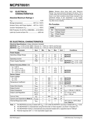
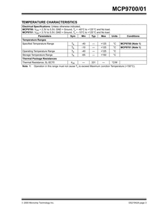
MCP9700/01
             Low-Power Voltage Output Temperature Sensor
Features                                                   Description
• Tiny Analog Temperature Sensor                           The MCP9700/01 low-cost, low-power and tiny tem-
• Available Packages: SC70-5                               perature sensor family converts temperature to an
• Wide Temperature Measurement Range:                      analog voltage. It provides an accuracy of ±4°C from
                                                           0°C to +70°C while consuming 6 µA (typ.) of operating
  - -40°C to +125°C
                                                           current.
• Accuracy: ±4°C (max.), 0°C to +70°C
                                                           The MCP9700/01 provides a low-cost solution for
• Optimized for Analog-to-Digital Converters
                                                           applications that require measurement of a relative
  (ADCs):
                                                           change of temperature. When measuring relative
  - MCP9700: 10.0 mV/°C (typ.)                             change in temperature from 25°C, an accuracy of
  - MCP9701: 19.5 mV/°C (typ.)                             ±1°C (typ.) can be realized from 0°C to 70°C. This
• Wide Operating Voltage Range:                            accuracy can also be achieved by applying system
  - MCP9700: VDD = 2.3V to 5.5V                            calibration at 25°C.
  - MCP9701: VDD = 3.1V to 5.5V                            Unlike resistive sensors such as thermistors, this
• Low Operating Current: 6 µA (typ.)                       family does not require a signal conditioning circuit.
                                                           The voltage output pin can be directly connected to an
• Optimized to Drive Large Capacitive Loads
                                                           ADC input of a microcontroller. The MCP9700 and
                                                           MCP9701 temperature coefficients are scaled to
Typical Applications                                       provide a 1° C/bit resolution for an 8-bit ADC with a
•   Hard Disk Drives and Other PC Peripherals              reference voltage of 2.5V and 5V, respectively.
•   Entertainment Systems                                  In addition, this family is immune to the effects of
•   Home Appliance                                         parasitic capacitance and can drive large capacitive
                                                           loads. This provides Printed Circuit Board (PCB) layout
•   Office Equipment
                                                           design flexibility by enabling the device to be remotely
•   Battery Packs and Portable Equipment                   located from the microcontroller. Adding some
•   General Purpose Temperature Monitoring                 capacitance at the output also helps the output
                                                           transient response by reducing overshoots or
                                                           undershoots. However, capacitive load is not required
                                                           for sensor output stability.

                                                           Package Type
                                                             SC70-5
                                                                             NC 1              5 NC
                                                                                     MCP9700
                                                                                     MCP9701


                                                                            GND 2
                                                                            VOUT 3             4 VDD


Typical Application Circuit
                                         PICmicro®
                            VDD        Microcontroller        MCP9700/01 VDD
                                    VDD
                                                                      VDD
                      10 kΩ                          ANI                              Cbypass
                                   MCLR                        VOUT
                                                                                      0.1 µF
                                    VSS
                                                                      GND


© 2005 Microchip Technology Inc.                                                                  DS21942A-page 1
MCP9700/01
1.0          ELECTRICAL                                                            †Notice: Stresses above those listed under “Maximum
                                                                                   Ratings” may cause permanent damage to the device. This is
             CHARACTERISTICS                                                       a stress rating only and functional operation of the device at
                                                                                   those or any other conditions above those indicated in the
Absolute Maximum Ratings †                                                         operational listings of this specification is not implied.
                                                                                   Exposure to maximum rating conditions for extended periods
VDD:...................................................................... 6.0V    may affect device reliability.
Storage temperature: ........................ -65°C to +150°C
                                                                                   Pin Function
Ambient Temp. with Power Applied:.. -40°C to +125°C
Junction Temperature (TJ):................................. 150°C                      NAME                       FUNCTION
ESD Protection On All Pins: (HBM:MM):... (4 kV:200V)                                     NC      Not Connected
Latch-Up Current at Each Pin: ...................... ±200 mA                            VOUT     Voltage Output
                                                                                        VDD      Power Supply
                                                                                        GND      Ground


DC ELECTRICAL CHARACTERISTICS
 Electrical Specifications: Unless otherwise indicated:
 MCP9700: VDD = 2.3V to 5.5V, GND = Ground, TA = -40°C to +125°C and No load.
 MCP9701: VDD = 3.1V to 5.5V, GND = Ground, TA = -10°C to +125°C and No load.
                   Parameter                              Sym              Min    Typ          Max     Unit              Conditions
 Power Supply
 Operating Voltage Range                                   VDD             2.3    —            5.5      V      MCP9700
                                                           VDD             3.1    —            5.5      V      MCP9701
 Operating Current                                         IDD              —      6           12       µA
 Power Supply Rejection                                   PSR               —     0.1          —       °C/V    MCP9700 VDD = 2.3V - 4.0V
                                                                                                               MCP9701 VDD = 3.1V - 4.0V
 Sensor Accuracy (Notes 1, 2)
    TA = +25°C                                            TACY              —     ±1            —       °C
    TA = 0°C to +70°C                                     TACY             -4.0   —            +4.0     °C
    TA = -40°C to +125°C                                  TACY             -4.0   —            +6.0     °C     MCP9700
    TA = -10°C to +125°C                                  TACY             -4.0   —            +6.0     °C     MCP9701
 Sensor Output
 Output Voltage:
  TA = 0°C                                                V0°C              —     500          —       mV      MCP9700
  TA = 0°C                                                V0°C              —     400          —       mV      MCP9701
 Temperature Coefficient                                   TC1              —     10.0         —      mV/°C MCP9700
                                                           TC1              —     19.5         —      mV/°C MCP9701
 Output Non-linearity                                     VONL              —     ±0.5         —        °C     TA = 0°C to +70°C (Note 2)
 Output Current                                           IOUT              —     —            100      µA
 Output Impedance                                         ZOUT              —     20           —        Ω      IOUT = 100 µA, f = 500 Hz
 Output Load Regulation                                 ΔVOUT/              —      1           —        Ω      TA = 0°C to +70°C,
                                                         ΔIOUT                                                 IOUT = 100 µA
 Turn-on Time                                              tON              —     800          —        µs
 Typical Load Capacitance (Note 3)                       CLOAD              —     —        1000         pF
 Thermal Response to 63%                                  tRES              —     1.3          —         s     30°C (air) to +125°C (fluid
                                                                                                               bath) (Note 4)
 Note 1:        The MCP9700 accuracy is tested with VDD = 3.3V, while the MCP9701 accuracy is tested with VDD = 5.0V.
      2:        The MCP9700/01 is characterized using the first-order or linear equation, as shown in Equation 3-1.
      3:        The MCP9700/01 family is characterized and production-tested with a capacitive load of 1000 pF.
      4:        Thermal response with 1 x 1 inch dual-sided copper clad.


DS21942A-page 2                                                                                               © 2005 Microchip Technology Inc.
MCP9700/01

TEMPERATURE CHARACTERISTICS
Electrical Specifications: Unless otherwise indicated,
MCP9700: VDD = 2.3V to 5.5V, GND = Ground, TA = -40°C to +125°C and No load.
MCP9701: VDD = 3.1V to 5.5V, GND = Ground, TA = -10°C to +125°C and No load.
                Parameters                  Sym       Min      Typ     Max       Units        Conditions
Temperature Ranges
Specified Temperature Range                  TA       -40      —       +125       °C     MCP9700 (Note 1)
                                             TA       -10      —       +125       °C     MCP9701 (Note 1)
Operating Temperature Range                  TA       -40      —       +125       °C
Storage Temperature Range                    TA       -65      —       +150       °C
Thermal Package Resistances
Thermal Resistance, 5L-SC70                  θJA       —       331      —        °C/W
Note 1:     Operation in this range must not cause TJ to exceed Maximum Junction Temperature (+150°C).


© 2005 Microchip Technology Inc.                                                                DS21942A-page 3
MCP9700/01
2.0                       TYPICAL PERFORMANCE CURVES
  Note:                         The graphs and tables provided following this note are a statistical summary based on a limited number of
                                samples and are provided for informational purposes only. The performance characteristics listed herein
                                are not tested or guaranteed. In some graphs or tables, the data presented may be outside the specified
                                operating range (e.g., outside specified power supply range) and therefore outside the warranted range.
Note: Unless otherwise indicated, MCP9700: VDD = 2.3V to 5.5V; MCP9701: VDD = 3.1V to 5.5V; GND = Ground,
Cbypass = 0.1 µF.

                   6.0                                                                                                                        0.2


                                                                                                             Accuracy Due to Load (°C)
                                                                                                                                                                                   MCP9701
                   4.0                                                                                                                                                              VDD = 5.0V
                                MCP9701                                                                                                       0.1
   Accuracy (°C)


                                 VDD= 5.0V                      Spec. Limits
                   2.0
                                                                                                                                                0
                   0.0                                                                                                                                                                  MCP9700
                                                                                                                                                                                        VDD = 3.3V
                                                                                                                                           -0.1
                   -2.0
                                MCP9700
                                 VDD= 3.3V                                                                                                                                                      ILOAD = 100 µA
                   -4.0                                                                                                                    -0.2
                          -50      -25       0      25     50   75     100        125                                                               -50     -25         0    25     50      75       100    125
                                                     TA (°C)                                                                                                                  TA (°C)

FIGURE 2-1:                                      Accuracy vs. Ambient                   FIGURE 2-4:       Changes in Accuracy vs.
Temperature.                                                                            Ambient Temperature (Due to Load).

                    6.0                                                                                                                  4.0
                                                                                                                                                    MCP9700/01
                                                                                            Load Regulation V/ I ( )


                                          MCP9700                    MCP9701                                                                         VDD = 3.3V
                    4.0                    VDD = 5.5V                 VDD= 5.5V                                                          3.0
   Accuracy (°C)


                                           VDD = 2.3V                 VDD= 3.1V                                                                     IOUT = 50 µA
                    2.0                                                                                                                             IOUT = 100 µA
                                                                                                                                         2.0        IOUT = 200 µA
                    0.0

                                                                                                                                         1.0
                   -2.0

                   -4.0                                                                                                                  0.0
                          -50      -25       0      25     50   75     100        125                                                          -50        -25       0       25     50      75        100    125
                                                     TA (°C)                                                                                                                 TA (°C)


FIGURE 2-2:        Accuracy vs. Ambient                                                 FIGURE 2-5:       Load Regulation vs.
Temperature, with VDD.                                                                  Ambient Temperature.

                   12.0                                                                                          1000
                                                                                                                                                    VDD = 5.0V
                   10.0                           MCP9701                                                                                           IOUT = 100 µA
                                                                                          Output Impedance ( )


                                                                                                                                                    TA = 26°C
                    8.0                                                                                                     100
   IDD (µA)


                    6.0
                                                                MCP9700
                    4.0
                                                                                                                                         10
                    2.0

                    0.0
                                                                                                                                          1
                          -50       -25      0      25     50   75     100        125                                                         0.1          1        10     100     1K            10K  100K
                                                                                                                                              0.1          1        10     100    1000          10000 100000
                                                     TA (°C)                                                                                                          Frequency (Hz)


FIGURE 2-3:                                      Supply Current vs.                     FIGURE 2-6:                                                                     Output Impedance vs.
Temperature.                                                                            Frequency.


DS21942A-page 4                                                                                                                                                         © 2005 Microchip Technology Inc.
MCP9700/01
Note: Unless otherwise indicated, MCP9700: VDD = 2.3V to 5.5V; MCP9701: VDD = 3.1V to 5.5V; GND = Ground,
Cbypass = 0.1 µF.


                 35%                                                                                                   35%
                        MCP9700                                                                                               MCP9701
                 30%    VDD = 3.3V                                                                                     30%    VDD = 5.0V
                        108 samples                                                                                           108 samples
                 25%                                                                                                   25%
   Occurrences


                                                                                                         Occurrences
                 20%                                                                                                   20%

                 15%                                                                                                   15%

                 10%                                                                                                   10%

                 5%                                                                                                    5%

                 0%                                                                                                    0%


                                                                                                                             300

                                                                                                                                      320

                                                                                                                                             340

                                                                                                                                                    360

                                                                                                                                                           380

                                                                                                                                                                  400

                                                                                                                                                                          420

                                                                                                                                                                                 440

                                                                                                                                                                                        460

                                                                                                                                                                                               480

                                                                                                                                                                                                      500
                       400

                                420

                                       440

                                              460

                                                     480

                                                            500

                                                                    520

                                                                           540

                                                                                  560

                                                                                         580

                                                                                                600
                                                        V0°C (mV)                                                                                             V0°C (mV)


FIGURE 2-7:                                    Output Voltage at 0°C                                   FIGURE 2-10:       Occurrences vs.
(MCP9700).                                                                                             Temperature Coefficient (MCP9701).

                 45%                                                                                                   45%
                             MCP9700                                                                                               MCP9701
                 40%         VDD = 3.3V
                                                                                                                       40%         VDD = 5.0V
                 35%         108 samples                                                                               35%         108 samples
                 30%                                                                                                   30%
   Occurrences


                                                                                                         Occurrences
                 25%                                                                                                   25%
                 20%                                                                                                   20%
                 15%                                                                                                   15%
                 10%                                                                                                   10%
                 5%                                                                                                    5%
                 0%                                                                                                    0%
                       9.5

                                9.6

                                       9.7

                                              9.8

                                                     9.9

                                                            10.0

                                                                    10.1

                                                                           10.2

                                                                                  10.3

                                                                                         10.4

                                                                                                10.5


                                                                                                                             19.0

                                                                                                                                      19.1

                                                                                                                                             19.2

                                                                                                                                                    19.3

                                                                                                                                                           19.4

                                                                                                                                                                  19.5

                                                                                                                                                                          19.6

                                                                                                                                                                                 19.7

                                                                                                                                                                                        19.8

                                                                                                                                                                                               19.9

                                                                                                                                                                                                      20.0
                                                     TC1 (mV/°C)                                                                                           TC1 (mV/°C)


FIGURE 2-8:        Occurrences vs. First-Order                                                         FIGURE 2-11:       Occurrences vs. First-Order
Temperature Coefficient (MCP9700).                                                                     Temperature Coefficient (MCP9701).

                 40%                                                                                                   40%
                          MCP9700                                                                                               MCP9701
                 35%                                                                                                   35%
                          VDD = 3.3V                                                                                            VDD = 3.3V
                 30%      108 samples                                                                                  30%      108 samples
   Occurrences


                                                                                                         Occurrences


                 25%                                                                                                   25%

                 20%                                                                                                   20%

                 15%                                                                                                   15%

                 10%                                                                                                   10%

                 5%                                                                                                    5%

                 0%                                                                                                    0%
                       -2.7

                                -2.4

                                       -2.1

                                              -1.8

                                                     -1.5

                                                            -1.2

                                                                    -0.9

                                                                           -0.6

                                                                                  -0.3

                                                                                         0.0

                                                                                                0.3


                                                                                                                             -4.3

                                                                                                                                      -4.0

                                                                                                                                             -3.7

                                                                                                                                                    -3.4

                                                                                                                                                           -3.1

                                                                                                                                                                  -2.8

                                                                                                                                                                          -2.5

                                                                                                                                                                                 -2.2

                                                                                                                                                                                        -1.9

                                                                                                                                                                                               -1.6

                                                                                                                                                                                                      -1.3


                                                                   2                                                                                                     2
                                                     TC2 (µV/°C )                                                                                          TC2 (µV/°C )


FIGURE 2-9:       Occurrences vs. Second-                                                              FIGURE 2-12:      Occurrences vs. Second-
Order Temperature Coefficient (MCP9700).                                                               Order Temperature Coefficient (MCP9701).


© 2005 Microchip Technology Inc.                                                                                                                                                 DS21942A-page 5
MCP9700/01
Note: Unless otherwise indicated, MCP9700: VDD = 2.3V to 5.5V; MCP9701: VDD = 3.1V to 5.5V; GND = Ground,
Cbypass = 0.1 µF.


                           0.30                                                                    3.0
                                    MCP9700
                                     VDD= 2.3V to 5.5V
                           0.25                                                                    2.5
   Normalized PSR (°C/V)


                           0.20                                                                    2.0


                                                                                        VOUT (V)
                           0.15                                                                    1.5

                           0.10     MCP9700                                                        1.0                                                                  MCP9700
                                     VDD= 2.3V to 4.0V                                                                                                                  MCP9701
                           0.05                                                                    0.5

                           0.00                                                                    0.0
                                  -50   -25      0       25     50   75   100   125                      -50          -25          0         25       50          75      100         125
                                                          TA (°C)                                                                              TA (°C)


FIGURE 2-13:       Power Supply Rejection                                             FIGURE 2-16:                                     Output Voltage vs. Ambient
(PSR) vs. Ambient Temperature.                                                        Temperature.

                           0.30
                                    MCP9701                                                        12                                                                               2.5
                                     VDD= 3.1V to 5.5V                                                                                                      VDD_STEP = 5V


                                                                                                                                                                                           IDD (mA)
                           0.25                                                                                                                                TA = 26°C
   Normalized PSR (°C/V)


                                                                                                   10                                                                               1.7
                                                                                                                                       IDD
                           0.20                                                                     8                                                                               0.8
                           0.15                                                                     6                                                                               0.0
                                                                                                                                         VOUT
                                                                                        VOUT (V)


                           0.10     MCP9701                                                         4                                                                               -0.8
                                     VDD= 3.1V to 4.0V
                           0.05                                                                     2                                                                               -1.7

                           0.00                                                                     0                                                                               -2.5
                                                                                                         -0.1
                                                                                                                0.0
                                                                                                                      0.1
                                                                                                                             0.2
                                                                                                                                   0.3
                                                                                                                                         0.4
                                                                                                                                                0.5
                                                                                                                                                      0.6
                                                                                                                                                            0.7
                                                                                                                                                                  0.8
                                                                                                                                                                        0.9
                                                                                                                                                                              1.0
                                  -50   -25      0       25     50   75   100   125
                                                          TA (°C)                                                                      Time (ms)


FIGURE 2-14:       Power Supply Rejection                                             FIGURE 2-17:                                     Output vs. Time.
(PSR) vs. Frequency.


                           1.6                                                                     3.0                                                                         30.0
                                   TA = 26°C                                                                                                      VDD_RAMP = 5V/ms
                           1.4


                                                                                                                                                                                           IDD (µA)
                                                                                                   2.5                 IDD                               TA = 26°C             18.0
                           1.2
                                                                                                   2.0                                                                         6.0
                           1.0
   VOUT (V)


                           0.8                                                                     1.5                                                                         -6.0
                                                                                        VOUT (V)


                           0.6                                                                                        VOUT
                                                                                                   1.0                                                                         -18.0
                           0.4
                                                                                                   0.5                                                                         -30.0
                           0.2
                           0.0                                                                     0.0                                                                         -42.0
                                 0.0 0.5 1.0 1.5 2.0 2.5 3.0 3.5 4.0 4.5 5.0 5.5                         0.0 0.1 0.2 0.3 0.4 0.5 0.6 0.7 0.8 0.9 1.0
                                                         VDD (V)                                                          Time (ms)


FIGURE 2-15:                                         Output Voltage vs. Power         FIGURE 2-18:                                     Output vs. Time
Supply.


DS21942A-page 6                                                                                                                          © 2005 Microchip Technology Inc.
MCP9700/01
Note: Unless otherwise indicated, MCP9700: VDD = 2.3V to 5.5V; MCP9701: VDD = 3.1V to 5.5V; GND = Ground,
Cbypass = 0.1 µF.


                 130


                 105
   Output (°C)


                  80


                  55                                                   SC70-5
                                              30°C (Air) to 125°C (Fluid bath)
                                                     1 in. x 1 in. copper clad
                  30
                       -2   0   2   4    6      8    10    12    14    16    18
                                             Time (s)


FIGURE 2-19:                            Thermal Response.


© 2005 Microchip Technology Inc.                                                             DS21942A-page 7
MCP9700/01
3.0      FUNCTIONAL DESCRIPTION
The MCP9700/01 temperature sensing element is
essentially a P-N junction or a diode. The diode electri-
cal characteristics has a temperature coefficient that
provides a change in voltage based on the relative
ambient temperature from -40°C to 125°C. The change
in voltage is scaled to a temperature coefficient of
10.0 mV/°C (typ.) for the MCP9700 and 19.5 mV/°C
(typ.) for the MCP9701. The output voltage at 0°C is
also scaled to 500 mV (typ.) and 400 mV (typ.) for the
MCP9700 and MCP9701, respectively. This linear
scale is described in the transfer function shown in
Equation 3-1.

EQUATION 3-1:           SENSOR TRANSFER
                        FUNCTION
                V OUT = T C1 • T A + V 0°C

      Where:
          TA    = Ambient Temperature
          VOUT = Sensor Output Voltage
          V0°C = Sensor Output Voltage at 0°C
          TC1   = Temperature Coefficient


DS21942A-page 8                                             © 2005 Microchip Technology Inc.
MCP9700/01
4.0                    APPLICATIONS INFORMATION                               4.2      Shutdown Using Microcontroller
                                                                                       I/O Pin
4.1                    Improving Accuracy
                                                                              The MCP9700/01 low operating current of 6 µA (typ.)
The MCP9700/01 accuracy can be improved by                                    makes it ideal for battery-powered applications.
performing a system calibration at a specific tempera-                        However, for applications that require tighter current
ture. For example, calibrating the system at 25°C                             budget, this device can be powered using a microcon-
ambient improves the measurement accuracy to a                                troller Input/Output (I/O) pin. The I/O pin can be toggled
±0.5°C (typ.) from 0°C to 70°C, as shown in Figure 4-1.                       to shutdown the device. In such applications, the
Therefore, when measuring relative temperature                                microcontroller internal digital switching noise is
change, this family measures temperature with higher                          emitted to the MCP9700/01 as power supply noise.
accuracy.                                                                     This switching noise compromises measurement
                                                                              accuracy. Therefore, a decoupling capacitor will be
                                                                              necessary.
                    3.0

                    2.0                                                       4.3      Layout Considerations
   Accuracy (°C)


                    1.0
                                                                              The MCP9700/01 does not require any additional
                    0.0                                                       components to operate. However, it is recommended
                                                                              that a decoupling capacitor of 0.1 µF to 1 µF be used
                    -1.0
                                                                              between the VDD and GND pins. In high-noise applica-
                    -2.0     VDD= 3.3V
                                                                              tions, connect the power supply voltage to the VDD pin
                             10 Samples
                    -3.0                                                      using a 200Ω resistor with a 1 µF decoupling capacitor.
                           -50   -25      0      25     50   75   100   125   A high-frequency ceramic capacitor is recommended. It
                                                  TA (°C)                     is necessary for the capacitor to be located as close as
                                                                              possible to the VDD and GND pins in order to provide
FIGURE 4-1:                                   Relative Accuracy to +25°C      effective noise protection. In addition, avoid tracing dig-
vs. Temperature.                                                              ital lines in close proximity to the sensor.

The relative change in accuracy from the calibration
temperature is due to the output non-linearity from the
first-order equation, specified in Equation 3-1. The
accuracy can be further improved by compensating for
the output non-linearity.
For higher accuracy, the sensor output transfer function
is also derived using a second-order equation as
shown in Equation 4-1. The equation describes the
output non-linearity. This equation is not used to
characterize the part as specified in the DC Electrical
Characteristics table; however, it provides better
accuracy.

EQUATION 4-1:                                 SECOND-ORDER
                                              TRANSFER FUNCTION
  VOUT = TC2 (TA + 10°C)(125°C – TA) + TC1 TA + V0°C
                     = -TC2 TA2 + (TC1 + 115 TC2)TA + 1250 TC2 + V0°C


                   Where:
                           TA   = Ambient Temperature
                           VOUT = Sensor Output Voltage
                           V0°C = Sensor Output Voltage at 0°C
                                  (refer to Figure 2-7 and 2-10)
                           TC1 = Temperature Coefficient
                                  (refer to Figure 2-8 and 2-11)
                           TC2 = Temperature Coefficient
                                     MCP9700 1.4 µV/°C2 (typ.)
                                     MCP9701 2.7 µV/°C2 (typ.)
                                  (refer to Figure 2-9 and 2-12)


© 2005 Microchip Technology Inc.                                                                                      DS21942A-page 9
MCP9700/01
4.4        Thermal Considerations
The MCP9700/01 measures temperature by monitor-
ing the voltage of a diode located in the die. A low
impedance thermal path between the die and the PCB
is provided by the pins. Therefore, the MCP9700/01
effectively monitors the temperature of the PCB.
However, the thermal path for the ambient air is not as
efficient because the plastic device package functions
as a thermal insulator from the die. This limitation
applies to plastic-packaged silicon temperature
sensors. If the application requires measuring ambient
air, the PCB needs to be designed with proper thermal
conduction to the sensor pins.
The MCP9700/01 is designed to source/sink 100 µA
(max.). The power dissipation due to the output current
is relatively insignificant. The effect of the output
current can be described using Equation 4-2.

EQUATION 4-2:               EFFECT OF SELF-
                            HEATING
      T J – T A = θ JA ( V DD I DD + ( V DD – V OUT ) I OUT )

 Where:
  TJ   = Junction Temperature
  TA = Ambient Temperature
  θJA = Package Thermal Resistance (331°C/W)
  VOUT = Sensor Output Voltage
  IOUT = Sensor Output Current
  IDD = Operating Current
  VDD = Operating Voltage

At TA = +25°C (VOUT = 0.75V) and maximum specifica-
tion of IDD = 12 µA, VDD = 5.5V and IOUT = +100 µA,
the self-heating due to power dissipation (TJ – TA) is
0.179°C.


DS21942A-page 10                                                © 2005 Microchip Technology Inc.
MCP9700/01
5.0      PACKAGING INFORMATION
5.1      Package Marking Information
             5-Lead SC-70 (MCP9700)                                               Example:


                 XXN (Front)                  Device             Code               AU2 (Front)
                 YWW (Back)              MCP9700                 AUN                548 (Back)
                                         MCP9701                  AVN
                                          Note: Applies to 5-Lead SC-70.


             5-Lead SC-70 (MCP9701)                                               Example:


                                              Device             Code
                     XXNN                MCP9700                 AUNN                   AV25
                                         MCP9701                 AVNN
                                          Note: Applies to 5-Lead SC-70.


                Legend: XX...X      Customer-specific information
                        Y           Year code (last digit of calendar year)
                        YY          Year code (last 2 digits of calendar year)
                        WW          Week code (week of January 1 is week ‘01’)
                        NNN         Alphanumeric traceability code
                            e3      Pb-free JEDEC designator for Matte Tin (Sn)
                           *        This package is Pb-free. The Pb-free JEDEC designator ( e3 )
                                    can be found on the outer packaging for this package.

                Note:    In the event the full Microchip part number cannot be marked on one line, it will
                         be carried over to the next line, thus limiting the number of available
                         characters for customer-specific information.


© 2005 Microchip Technology Inc.                                                                       DS21942A-page 11
MCP9700/01
5-Lead Plastic Small Outline Transistor (LT) (SC-70)


                                       E
                                       E1


                                                                      D

                p                                             B


                        n                             1


              Q1

                                                                                A2                                       A
       c


                                                                           A1


                                                          L


                                          Units                     INCHES                         MILLIMETERS*
                               Dimension Limits       MIN             NOM        MAX         MIN        NOM        MAX
       Number of Pins                       n                           5                                  5
       Pitch                                p                     .026 (BSC)                         0.65 (BSC)
       Overall Height                       A             .031                       .043       0.80                   1.10
       Molded Package Thickness             A2            .031                       .039       0.80                   1.00
       Standoff                             A1            .000                       .004       0.00                   0.10
       Overall Width                        E             .071                       .094       1.80                   2.40
       Molded Package Width                 E1            .045                       .053       1.15                   1.35
       Overall Length                       D             .071                       .087       1.80                   2.20
       Foot Length                           L            .004                       .012       0.10                   0.30
       Top of Molded Pkg to Lead Shoulder   Q1            .004                       .016       0.10                   0.40
       Lead Thickness                        c            .004                       .007       0.10                   0.18
       Lead Width                            B            .006                       .012       0.15                   0.30


           *Controlling Parameter
           Notes:
             Dimensions D and E1 do not include mold flash or protrusions. Mold flash or protrusions shall not
             exceed .005" (0.127mm) per side.

       JEITA (EIAJ) Standard: SC-70
       Drawing No. C04-061


DS21942A-page 12                                                                                      © 2005 Microchip Technology Inc.
MCP9700/01
APPENDIX A:            REVISION HISTORY

Revision A (March 2005)
• Original Release of this Document.


© 2005 Microchip Technology Inc.              DS21942A-page 11
MCP9700/01
NOTES:


DS21942A-page 12   © 2005 Microchip Technology Inc.
MCP9700/01
PRODUCT IDENTIFICATION SYSTEM
To order or obtain information, e.g., on pricing or delivery, refer to the factory or the listed sales office.

  PART NO.        –    X              /XX                                               Examples:
                                                                                        a)    MCP9700T-E/LT:     Tiny Analog Temperature
    Device       Temperature        Package                                                                      Sensor, Tape and Reel,
                   Range                                                                                         -40°C to +125°C,
                                                                                                                 5LD SC70 package.

  Device:               MCP9700T: Tiny Analog Temperature Sensor,
                                  Tape and Reel, Pb free                                a)    MCP9701T-E/LT:     Tiny Analog Temperature
                        MCP9701T: Tiny Analog Temperature Sensor,                                                Sensor, Tape and Reel,
                                  Tape and Reel, Pb free                                                         -40°C to +125°C,
                                                                                                                 5LD SC70 package.

  Temperature           E   = -40°C to +125°C
  Range:


  Package:              LT =   Plastic Small Outline Transistor, 5-lead


© 2005 Microchip Technology Inc.                                                                                        DS21942A-page 13
MCP9700/01
NOTES:


DS21942A-page 14   © 2005 Microchip Technology Inc.
Note the following details of the code protection feature on Microchip devices:
•    Microchip products meet the specification contained in their particular Microchip Data Sheet.

•    Microchip believes that its family of products is one of the most secure families of its kind on the market today, when used in the
     intended manner and under normal conditions.

•    There are dishonest and possibly illegal methods used to breach the code protection feature. All of these methods, to our
     knowledge, require using the Microchip products in a manner outside the operating specifications contained in Microchip’s Data
     Sheets. Most likely, the person doing so is engaged in theft of intellectual property.

•    Microchip is willing to work with the customer who is concerned about the integrity of their code.

•    Neither Microchip nor any other semiconductor manufacturer can guarantee the security of their code. Code protection does not
     mean that we are guaranteeing the product as “unbreakable.”

Code protection is constantly evolving. We at Microchip are committed to continuously improving the code protection features of our
products. Attempts to break Microchip’s code protection feature may be a violation of the Digital Millennium Copyright Act. If such acts
allow unauthorized access to your software or other copyrighted work, you may have a right to sue for relief under that Act.


Information contained in this publication regarding device               Trademarks
applications and the like is provided only for your convenience          The Microchip name and logo, the Microchip logo, Accuron,
and may be superseded by updates. It is your responsibility to           dsPIC, KEELOQ, microID, MPLAB, PIC, PICmicro, PICSTART,
ensure that your application meets with your specifications.
                                                                         PRO MATE, PowerSmart, rfPIC, and SmartShunt are
MICROCHIP MAKES NO REPRESENTATIONS OR WAR-
                                                                         registered trademarks of Microchip Technology Incorporated
RANTIES OF ANY KIND WHETHER EXPRESS OR IMPLIED,
                                                                         in the U.S.A. and other countries.
WRITTEN OR ORAL, STATUTORY OR OTHERWISE,
RELATED TO THE INFORMATION, INCLUDING BUT NOT                            AmpLab, FilterLab, Migratable Memory, MXDEV, MXLAB,
LIMITED TO ITS CONDITION, QUALITY, PERFORMANCE,                          PICMASTER, SEEVAL, SmartSensor and The Embedded
MERCHANTABILITY OR FITNESS FOR PURPOSE.                                  Control Solutions Company are registered trademarks of
Microchip disclaims all liability arising from this information and      Microchip Technology Incorporated in the U.S.A.
its use. Use of Microchip’s products as critical components in           Analog-for-the-Digital Age, Application Maestro, dsPICDEM,
life support systems is not authorized except with express               dsPICDEM.net, dsPICworks, ECAN, ECONOMONITOR,
written approval by Microchip. No licenses are conveyed,                 FanSense, FlexROM, fuzzyLAB, In-Circuit Serial
implicitly or otherwise, under any Microchip intellectual property       Programming, ICSP, ICEPIC, MPASM, MPLIB, MPLINK,
rights.                                                                  MPSIM, PICkit, PICDEM, PICDEM.net, PICLAB, PICtail,
                                                                         PowerCal, PowerInfo, PowerMate, PowerTool, rfLAB,
                                                                         rfPICDEM, Select Mode, Smart Serial, SmartTel, Total
                                                                         Endurance and WiperLock are trademarks of Microchip
                                                                         Technology Incorporated in the U.S.A. and other countries.
                                                                         SQTP is a service mark of Microchip Technology Incorporated
                                                                         in the U.S.A.
                                                                         All other trademarks mentioned herein are property of their
                                                                         respective companies.
                                                                         © 2005, Microchip Technology Incorporated, Printed in the
                                                                         U.S.A., All Rights Reserved.
                                                                              Printed on recycled paper.


                                                                         Microchip received ISO/TS-16949:2002 quality system certification for
                                                                         its worldwide headquarters, design and wafer fabrication facilities in
                                                                         Chandler and Tempe, Arizona and Mountain View, California in
                                                                         October 2003. The Company’s quality system processes and
                                                                         procedures are for its PICmicro® 8-bit MCUs, KEELOQ® code hopping
                                                                         devices, Serial EEPROMs, microperipherals, nonvolatile memory and
                                                                         analog products. In addition, Microchip’s quality system for the design
                                                                         and manufacture of development systems is ISO 9001:2000 certified.


© 2005 Microchip Technology Inc.                                                                                         DS21942A-page 15
WORLDWIDE SALES AND SERVICE
AMERICAS                        ASIA/PACIFIC            ASIA/PACIFIC                EUROPE
Corporate Office                Australia - Sydney      India - Bangalore           Austria - Weis
2355 West Chandler Blvd.        Tel: 61-2-9868-6733     Tel: 91-80-2229-0061        Tel: 43-7242-2244-399
Chandler, AZ 85224-6199         Fax: 61-2-9868-6755     Fax: 91-80-2229-0062        Fax: 43-7242-2244-393
Tel: 480-792-7200               China - Beijing                                     Denmark - Ballerup
                                                        India - New Delhi
Fax: 480-792-7277               Tel: 86-10-8528-2100                                Tel: 45-4450-2828
                                                        Tel: 91-11-5160-8631
Technical Support:              Fax: 86-10-8528-2104                                Fax: 45-4485-2829
                                                        Fax: 91-11-5160-8632
http://support.microchip.com
                                China - Chengdu         Japan - Kanagawa            France - Massy
Web Address:
                                Tel: 86-28-8676-6200    Tel: 81-45-471- 6166        Tel: 33-1-69-53-63-20
www.microchip.com
                                Fax: 86-28-8676-6599    Fax: 81-45-471-6122         Fax: 33-1-69-30-90-79
Atlanta
Alpharetta, GA                  China - Fuzhou          Korea - Seoul               Germany - Ismaning
                                Tel: 86-591-8750-3506   Tel: 82-2-554-7200          Tel: 49-89-627-144-0
Tel: 770-640-0034
                                Fax: 86-591-8750-3521   Fax: 82-2-558-5932 or       Fax: 49-89-627-144-44
Fax: 770-640-0307
                                China - Hong Kong SAR   82-2-558-5934               Italy - Milan
Boston
                                Tel: 852-2401-1200                                  Tel: 39-0331-742611
Westborough, MA                                         Singapore
                                Fax: 852-2401-3431      Tel: 65-6334-8870           Fax: 39-0331-466781
Tel: 774-760-0087
Fax: 774-760-0088               China - Shanghai        Fax: 65-6334-8850           Netherlands - Drunen
                                Tel: 86-21-5407-5533    Taiwan - Kaohsiung          Tel: 31-416-690399
Chicago
                                Fax: 86-21-5407-5066    Tel: 886-7-536-4818         Fax: 31-416-690340
Itasca, IL
Tel: 630-285-0071               China - Shenyang        Fax: 886-7-536-4803         England - Berkshire
Fax: 630-285-0075               Tel: 86-24-2334-2829                                Tel: 44-118-921-5869
                                                        Taiwan - Taipei
                                Fax: 86-24-2334-2393    Tel: 886-2-2500-6610        Fax: 44-118-921-5820
Dallas
Addison, TX                     China - Shenzhen        Fax: 886-2-2508-0102
Tel: 972-818-7423               Tel: 86-755-8203-2660   Taiwan - Hsinchu
Fax: 972-818-2924               Fax: 86-755-8203-1760   Tel: 886-3-572-9526
Detroit                         China - Shunde          Fax: 886-3-572-6459
Farmington Hills, MI            Tel: 86-757-2839-5507
Tel: 248-538-2250               Fax: 86-757-2839-5571
Fax: 248-538-2260               China - Qingdao
Kokomo                          Tel: 86-532-502-7355
Kokomo, IN                      Fax: 86-532-502-7205
Tel: 765-864-8360
Fax: 765-864-8387
Los Angeles
Mission Viejo, CA
Tel: 949-462-9523
Fax: 949-462-9608
San Jose
Mountain View, CA
Tel: 650-215-1444
Fax: 650-961-0286
Toronto
Mississauga, Ontario,
Canada
Tel: 905-673-0699
Fax: 905-673-6509


                                                                                                     03/01/05


DS21942A-page 16                                                                © 2005 Microchip Technology Inc.

Datasheet sensor temperatura mcp9700

  • 1.
    MCP9700/01 Low-Power Voltage Output Temperature Sensor Features Description • Tiny Analog Temperature Sensor The MCP9700/01 low-cost, low-power and tiny tem- • Available Packages: SC70-5 perature sensor family converts temperature to an • Wide Temperature Measurement Range: analog voltage. It provides an accuracy of ±4°C from 0°C to +70°C while consuming 6 µA (typ.) of operating - -40°C to +125°C current. • Accuracy: ±4°C (max.), 0°C to +70°C The MCP9700/01 provides a low-cost solution for • Optimized for Analog-to-Digital Converters applications that require measurement of a relative (ADCs): change of temperature. When measuring relative - MCP9700: 10.0 mV/°C (typ.) change in temperature from 25°C, an accuracy of - MCP9701: 19.5 mV/°C (typ.) ±1°C (typ.) can be realized from 0°C to 70°C. This • Wide Operating Voltage Range: accuracy can also be achieved by applying system - MCP9700: VDD = 2.3V to 5.5V calibration at 25°C. - MCP9701: VDD = 3.1V to 5.5V Unlike resistive sensors such as thermistors, this • Low Operating Current: 6 µA (typ.) family does not require a signal conditioning circuit. The voltage output pin can be directly connected to an • Optimized to Drive Large Capacitive Loads ADC input of a microcontroller. The MCP9700 and MCP9701 temperature coefficients are scaled to Typical Applications provide a 1° C/bit resolution for an 8-bit ADC with a • Hard Disk Drives and Other PC Peripherals reference voltage of 2.5V and 5V, respectively. • Entertainment Systems In addition, this family is immune to the effects of • Home Appliance parasitic capacitance and can drive large capacitive loads. This provides Printed Circuit Board (PCB) layout • Office Equipment design flexibility by enabling the device to be remotely • Battery Packs and Portable Equipment located from the microcontroller. Adding some • General Purpose Temperature Monitoring capacitance at the output also helps the output transient response by reducing overshoots or undershoots. However, capacitive load is not required for sensor output stability. Package Type SC70-5 NC 1 5 NC MCP9700 MCP9701 GND 2 VOUT 3 4 VDD Typical Application Circuit PICmicro® VDD Microcontroller MCP9700/01 VDD VDD VDD 10 kΩ ANI Cbypass MCLR VOUT 0.1 µF VSS GND © 2005 Microchip Technology Inc. DS21942A-page 1
  • 2.
    MCP9700/01 1.0 ELECTRICAL †Notice: Stresses above those listed under “Maximum Ratings” may cause permanent damage to the device. This is CHARACTERISTICS a stress rating only and functional operation of the device at those or any other conditions above those indicated in the Absolute Maximum Ratings † operational listings of this specification is not implied. Exposure to maximum rating conditions for extended periods VDD:...................................................................... 6.0V may affect device reliability. Storage temperature: ........................ -65°C to +150°C Pin Function Ambient Temp. with Power Applied:.. -40°C to +125°C Junction Temperature (TJ):................................. 150°C NAME FUNCTION ESD Protection On All Pins: (HBM:MM):... (4 kV:200V) NC Not Connected Latch-Up Current at Each Pin: ...................... ±200 mA VOUT Voltage Output VDD Power Supply GND Ground DC ELECTRICAL CHARACTERISTICS Electrical Specifications: Unless otherwise indicated: MCP9700: VDD = 2.3V to 5.5V, GND = Ground, TA = -40°C to +125°C and No load. MCP9701: VDD = 3.1V to 5.5V, GND = Ground, TA = -10°C to +125°C and No load. Parameter Sym Min Typ Max Unit Conditions Power Supply Operating Voltage Range VDD 2.3 — 5.5 V MCP9700 VDD 3.1 — 5.5 V MCP9701 Operating Current IDD — 6 12 µA Power Supply Rejection PSR — 0.1 — °C/V MCP9700 VDD = 2.3V - 4.0V MCP9701 VDD = 3.1V - 4.0V Sensor Accuracy (Notes 1, 2) TA = +25°C TACY — ±1 — °C TA = 0°C to +70°C TACY -4.0 — +4.0 °C TA = -40°C to +125°C TACY -4.0 — +6.0 °C MCP9700 TA = -10°C to +125°C TACY -4.0 — +6.0 °C MCP9701 Sensor Output Output Voltage: TA = 0°C V0°C — 500 — mV MCP9700 TA = 0°C V0°C — 400 — mV MCP9701 Temperature Coefficient TC1 — 10.0 — mV/°C MCP9700 TC1 — 19.5 — mV/°C MCP9701 Output Non-linearity VONL — ±0.5 — °C TA = 0°C to +70°C (Note 2) Output Current IOUT — — 100 µA Output Impedance ZOUT — 20 — Ω IOUT = 100 µA, f = 500 Hz Output Load Regulation ΔVOUT/ — 1 — Ω TA = 0°C to +70°C, ΔIOUT IOUT = 100 µA Turn-on Time tON — 800 — µs Typical Load Capacitance (Note 3) CLOAD — — 1000 pF Thermal Response to 63% tRES — 1.3 — s 30°C (air) to +125°C (fluid bath) (Note 4) Note 1: The MCP9700 accuracy is tested with VDD = 3.3V, while the MCP9701 accuracy is tested with VDD = 5.0V. 2: The MCP9700/01 is characterized using the first-order or linear equation, as shown in Equation 3-1. 3: The MCP9700/01 family is characterized and production-tested with a capacitive load of 1000 pF. 4: Thermal response with 1 x 1 inch dual-sided copper clad. DS21942A-page 2 © 2005 Microchip Technology Inc.
  • 3.
    MCP9700/01 TEMPERATURE CHARACTERISTICS Electrical Specifications:Unless otherwise indicated, MCP9700: VDD = 2.3V to 5.5V, GND = Ground, TA = -40°C to +125°C and No load. MCP9701: VDD = 3.1V to 5.5V, GND = Ground, TA = -10°C to +125°C and No load. Parameters Sym Min Typ Max Units Conditions Temperature Ranges Specified Temperature Range TA -40 — +125 °C MCP9700 (Note 1) TA -10 — +125 °C MCP9701 (Note 1) Operating Temperature Range TA -40 — +125 °C Storage Temperature Range TA -65 — +150 °C Thermal Package Resistances Thermal Resistance, 5L-SC70 θJA — 331 — °C/W Note 1: Operation in this range must not cause TJ to exceed Maximum Junction Temperature (+150°C). © 2005 Microchip Technology Inc. DS21942A-page 3
  • 4.
    MCP9700/01 2.0 TYPICAL PERFORMANCE CURVES Note: The graphs and tables provided following this note are a statistical summary based on a limited number of samples and are provided for informational purposes only. The performance characteristics listed herein are not tested or guaranteed. In some graphs or tables, the data presented may be outside the specified operating range (e.g., outside specified power supply range) and therefore outside the warranted range. Note: Unless otherwise indicated, MCP9700: VDD = 2.3V to 5.5V; MCP9701: VDD = 3.1V to 5.5V; GND = Ground, Cbypass = 0.1 µF. 6.0 0.2 Accuracy Due to Load (°C) MCP9701 4.0 VDD = 5.0V MCP9701 0.1 Accuracy (°C) VDD= 5.0V Spec. Limits 2.0 0 0.0 MCP9700 VDD = 3.3V -0.1 -2.0 MCP9700 VDD= 3.3V ILOAD = 100 µA -4.0 -0.2 -50 -25 0 25 50 75 100 125 -50 -25 0 25 50 75 100 125 TA (°C) TA (°C) FIGURE 2-1: Accuracy vs. Ambient FIGURE 2-4: Changes in Accuracy vs. Temperature. Ambient Temperature (Due to Load). 6.0 4.0 MCP9700/01 Load Regulation V/ I ( ) MCP9700 MCP9701 VDD = 3.3V 4.0 VDD = 5.5V VDD= 5.5V 3.0 Accuracy (°C) VDD = 2.3V VDD= 3.1V IOUT = 50 µA 2.0 IOUT = 100 µA 2.0 IOUT = 200 µA 0.0 1.0 -2.0 -4.0 0.0 -50 -25 0 25 50 75 100 125 -50 -25 0 25 50 75 100 125 TA (°C) TA (°C) FIGURE 2-2: Accuracy vs. Ambient FIGURE 2-5: Load Regulation vs. Temperature, with VDD. Ambient Temperature. 12.0 1000 VDD = 5.0V 10.0 MCP9701 IOUT = 100 µA Output Impedance ( ) TA = 26°C 8.0 100 IDD (µA) 6.0 MCP9700 4.0 10 2.0 0.0 1 -50 -25 0 25 50 75 100 125 0.1 1 10 100 1K 10K 100K 0.1 1 10 100 1000 10000 100000 TA (°C) Frequency (Hz) FIGURE 2-3: Supply Current vs. FIGURE 2-6: Output Impedance vs. Temperature. Frequency. DS21942A-page 4 © 2005 Microchip Technology Inc.
  • 5.
    MCP9700/01 Note: Unless otherwiseindicated, MCP9700: VDD = 2.3V to 5.5V; MCP9701: VDD = 3.1V to 5.5V; GND = Ground, Cbypass = 0.1 µF. 35% 35% MCP9700 MCP9701 30% VDD = 3.3V 30% VDD = 5.0V 108 samples 108 samples 25% 25% Occurrences Occurrences 20% 20% 15% 15% 10% 10% 5% 5% 0% 0% 300 320 340 360 380 400 420 440 460 480 500 400 420 440 460 480 500 520 540 560 580 600 V0°C (mV) V0°C (mV) FIGURE 2-7: Output Voltage at 0°C FIGURE 2-10: Occurrences vs. (MCP9700). Temperature Coefficient (MCP9701). 45% 45% MCP9700 MCP9701 40% VDD = 3.3V 40% VDD = 5.0V 35% 108 samples 35% 108 samples 30% 30% Occurrences Occurrences 25% 25% 20% 20% 15% 15% 10% 10% 5% 5% 0% 0% 9.5 9.6 9.7 9.8 9.9 10.0 10.1 10.2 10.3 10.4 10.5 19.0 19.1 19.2 19.3 19.4 19.5 19.6 19.7 19.8 19.9 20.0 TC1 (mV/°C) TC1 (mV/°C) FIGURE 2-8: Occurrences vs. First-Order FIGURE 2-11: Occurrences vs. First-Order Temperature Coefficient (MCP9700). Temperature Coefficient (MCP9701). 40% 40% MCP9700 MCP9701 35% 35% VDD = 3.3V VDD = 3.3V 30% 108 samples 30% 108 samples Occurrences Occurrences 25% 25% 20% 20% 15% 15% 10% 10% 5% 5% 0% 0% -2.7 -2.4 -2.1 -1.8 -1.5 -1.2 -0.9 -0.6 -0.3 0.0 0.3 -4.3 -4.0 -3.7 -3.4 -3.1 -2.8 -2.5 -2.2 -1.9 -1.6 -1.3 2 2 TC2 (µV/°C ) TC2 (µV/°C ) FIGURE 2-9: Occurrences vs. Second- FIGURE 2-12: Occurrences vs. Second- Order Temperature Coefficient (MCP9700). Order Temperature Coefficient (MCP9701). © 2005 Microchip Technology Inc. DS21942A-page 5
  • 6.
    MCP9700/01 Note: Unless otherwiseindicated, MCP9700: VDD = 2.3V to 5.5V; MCP9701: VDD = 3.1V to 5.5V; GND = Ground, Cbypass = 0.1 µF. 0.30 3.0 MCP9700 VDD= 2.3V to 5.5V 0.25 2.5 Normalized PSR (°C/V) 0.20 2.0 VOUT (V) 0.15 1.5 0.10 MCP9700 1.0 MCP9700 VDD= 2.3V to 4.0V MCP9701 0.05 0.5 0.00 0.0 -50 -25 0 25 50 75 100 125 -50 -25 0 25 50 75 100 125 TA (°C) TA (°C) FIGURE 2-13: Power Supply Rejection FIGURE 2-16: Output Voltage vs. Ambient (PSR) vs. Ambient Temperature. Temperature. 0.30 MCP9701 12 2.5 VDD= 3.1V to 5.5V VDD_STEP = 5V IDD (mA) 0.25 TA = 26°C Normalized PSR (°C/V) 10 1.7 IDD 0.20 8 0.8 0.15 6 0.0 VOUT VOUT (V) 0.10 MCP9701 4 -0.8 VDD= 3.1V to 4.0V 0.05 2 -1.7 0.00 0 -2.5 -0.1 0.0 0.1 0.2 0.3 0.4 0.5 0.6 0.7 0.8 0.9 1.0 -50 -25 0 25 50 75 100 125 TA (°C) Time (ms) FIGURE 2-14: Power Supply Rejection FIGURE 2-17: Output vs. Time. (PSR) vs. Frequency. 1.6 3.0 30.0 TA = 26°C VDD_RAMP = 5V/ms 1.4 IDD (µA) 2.5 IDD TA = 26°C 18.0 1.2 2.0 6.0 1.0 VOUT (V) 0.8 1.5 -6.0 VOUT (V) 0.6 VOUT 1.0 -18.0 0.4 0.5 -30.0 0.2 0.0 0.0 -42.0 0.0 0.5 1.0 1.5 2.0 2.5 3.0 3.5 4.0 4.5 5.0 5.5 0.0 0.1 0.2 0.3 0.4 0.5 0.6 0.7 0.8 0.9 1.0 VDD (V) Time (ms) FIGURE 2-15: Output Voltage vs. Power FIGURE 2-18: Output vs. Time Supply. DS21942A-page 6 © 2005 Microchip Technology Inc.
  • 7.
    MCP9700/01 Note: Unless otherwiseindicated, MCP9700: VDD = 2.3V to 5.5V; MCP9701: VDD = 3.1V to 5.5V; GND = Ground, Cbypass = 0.1 µF. 130 105 Output (°C) 80 55 SC70-5 30°C (Air) to 125°C (Fluid bath) 1 in. x 1 in. copper clad 30 -2 0 2 4 6 8 10 12 14 16 18 Time (s) FIGURE 2-19: Thermal Response. © 2005 Microchip Technology Inc. DS21942A-page 7
  • 8.
    MCP9700/01 3.0 FUNCTIONAL DESCRIPTION The MCP9700/01 temperature sensing element is essentially a P-N junction or a diode. The diode electri- cal characteristics has a temperature coefficient that provides a change in voltage based on the relative ambient temperature from -40°C to 125°C. The change in voltage is scaled to a temperature coefficient of 10.0 mV/°C (typ.) for the MCP9700 and 19.5 mV/°C (typ.) for the MCP9701. The output voltage at 0°C is also scaled to 500 mV (typ.) and 400 mV (typ.) for the MCP9700 and MCP9701, respectively. This linear scale is described in the transfer function shown in Equation 3-1. EQUATION 3-1: SENSOR TRANSFER FUNCTION V OUT = T C1 • T A + V 0°C Where: TA = Ambient Temperature VOUT = Sensor Output Voltage V0°C = Sensor Output Voltage at 0°C TC1 = Temperature Coefficient DS21942A-page 8 © 2005 Microchip Technology Inc.
  • 9.
    MCP9700/01 4.0 APPLICATIONS INFORMATION 4.2 Shutdown Using Microcontroller I/O Pin 4.1 Improving Accuracy The MCP9700/01 low operating current of 6 µA (typ.) The MCP9700/01 accuracy can be improved by makes it ideal for battery-powered applications. performing a system calibration at a specific tempera- However, for applications that require tighter current ture. For example, calibrating the system at 25°C budget, this device can be powered using a microcon- ambient improves the measurement accuracy to a troller Input/Output (I/O) pin. The I/O pin can be toggled ±0.5°C (typ.) from 0°C to 70°C, as shown in Figure 4-1. to shutdown the device. In such applications, the Therefore, when measuring relative temperature microcontroller internal digital switching noise is change, this family measures temperature with higher emitted to the MCP9700/01 as power supply noise. accuracy. This switching noise compromises measurement accuracy. Therefore, a decoupling capacitor will be necessary. 3.0 2.0 4.3 Layout Considerations Accuracy (°C) 1.0 The MCP9700/01 does not require any additional 0.0 components to operate. However, it is recommended that a decoupling capacitor of 0.1 µF to 1 µF be used -1.0 between the VDD and GND pins. In high-noise applica- -2.0 VDD= 3.3V tions, connect the power supply voltage to the VDD pin 10 Samples -3.0 using a 200Ω resistor with a 1 µF decoupling capacitor. -50 -25 0 25 50 75 100 125 A high-frequency ceramic capacitor is recommended. It TA (°C) is necessary for the capacitor to be located as close as possible to the VDD and GND pins in order to provide FIGURE 4-1: Relative Accuracy to +25°C effective noise protection. In addition, avoid tracing dig- vs. Temperature. ital lines in close proximity to the sensor. The relative change in accuracy from the calibration temperature is due to the output non-linearity from the first-order equation, specified in Equation 3-1. The accuracy can be further improved by compensating for the output non-linearity. For higher accuracy, the sensor output transfer function is also derived using a second-order equation as shown in Equation 4-1. The equation describes the output non-linearity. This equation is not used to characterize the part as specified in the DC Electrical Characteristics table; however, it provides better accuracy. EQUATION 4-1: SECOND-ORDER TRANSFER FUNCTION VOUT = TC2 (TA + 10°C)(125°C – TA) + TC1 TA + V0°C = -TC2 TA2 + (TC1 + 115 TC2)TA + 1250 TC2 + V0°C Where: TA = Ambient Temperature VOUT = Sensor Output Voltage V0°C = Sensor Output Voltage at 0°C (refer to Figure 2-7 and 2-10) TC1 = Temperature Coefficient (refer to Figure 2-8 and 2-11) TC2 = Temperature Coefficient MCP9700 1.4 µV/°C2 (typ.) MCP9701 2.7 µV/°C2 (typ.) (refer to Figure 2-9 and 2-12) © 2005 Microchip Technology Inc. DS21942A-page 9
  • 10.
    MCP9700/01 4.4 Thermal Considerations The MCP9700/01 measures temperature by monitor- ing the voltage of a diode located in the die. A low impedance thermal path between the die and the PCB is provided by the pins. Therefore, the MCP9700/01 effectively monitors the temperature of the PCB. However, the thermal path for the ambient air is not as efficient because the plastic device package functions as a thermal insulator from the die. This limitation applies to plastic-packaged silicon temperature sensors. If the application requires measuring ambient air, the PCB needs to be designed with proper thermal conduction to the sensor pins. The MCP9700/01 is designed to source/sink 100 µA (max.). The power dissipation due to the output current is relatively insignificant. The effect of the output current can be described using Equation 4-2. EQUATION 4-2: EFFECT OF SELF- HEATING T J – T A = θ JA ( V DD I DD + ( V DD – V OUT ) I OUT ) Where: TJ = Junction Temperature TA = Ambient Temperature θJA = Package Thermal Resistance (331°C/W) VOUT = Sensor Output Voltage IOUT = Sensor Output Current IDD = Operating Current VDD = Operating Voltage At TA = +25°C (VOUT = 0.75V) and maximum specifica- tion of IDD = 12 µA, VDD = 5.5V and IOUT = +100 µA, the self-heating due to power dissipation (TJ – TA) is 0.179°C. DS21942A-page 10 © 2005 Microchip Technology Inc.
  • 11.
    MCP9700/01 5.0 PACKAGING INFORMATION 5.1 Package Marking Information 5-Lead SC-70 (MCP9700) Example: XXN (Front) Device Code AU2 (Front) YWW (Back) MCP9700 AUN 548 (Back) MCP9701 AVN Note: Applies to 5-Lead SC-70. 5-Lead SC-70 (MCP9701) Example: Device Code XXNN MCP9700 AUNN AV25 MCP9701 AVNN Note: Applies to 5-Lead SC-70. Legend: XX...X Customer-specific information Y Year code (last digit of calendar year) YY Year code (last 2 digits of calendar year) WW Week code (week of January 1 is week ‘01’) NNN Alphanumeric traceability code e3 Pb-free JEDEC designator for Matte Tin (Sn) * This package is Pb-free. The Pb-free JEDEC designator ( e3 ) can be found on the outer packaging for this package. Note: In the event the full Microchip part number cannot be marked on one line, it will be carried over to the next line, thus limiting the number of available characters for customer-specific information. © 2005 Microchip Technology Inc. DS21942A-page 11
  • 12.
    MCP9700/01 5-Lead Plastic SmallOutline Transistor (LT) (SC-70) E E1 D p B n 1 Q1 A2 A c A1 L Units INCHES MILLIMETERS* Dimension Limits MIN NOM MAX MIN NOM MAX Number of Pins n 5 5 Pitch p .026 (BSC) 0.65 (BSC) Overall Height A .031 .043 0.80 1.10 Molded Package Thickness A2 .031 .039 0.80 1.00 Standoff A1 .000 .004 0.00 0.10 Overall Width E .071 .094 1.80 2.40 Molded Package Width E1 .045 .053 1.15 1.35 Overall Length D .071 .087 1.80 2.20 Foot Length L .004 .012 0.10 0.30 Top of Molded Pkg to Lead Shoulder Q1 .004 .016 0.10 0.40 Lead Thickness c .004 .007 0.10 0.18 Lead Width B .006 .012 0.15 0.30 *Controlling Parameter Notes: Dimensions D and E1 do not include mold flash or protrusions. Mold flash or protrusions shall not exceed .005" (0.127mm) per side. JEITA (EIAJ) Standard: SC-70 Drawing No. C04-061 DS21942A-page 12 © 2005 Microchip Technology Inc.
  • 13.
    MCP9700/01 APPENDIX A: REVISION HISTORY Revision A (March 2005) • Original Release of this Document. © 2005 Microchip Technology Inc. DS21942A-page 11
  • 14.
    MCP9700/01 NOTES: DS21942A-page 12 © 2005 Microchip Technology Inc.
  • 15.
    MCP9700/01 PRODUCT IDENTIFICATION SYSTEM Toorder or obtain information, e.g., on pricing or delivery, refer to the factory or the listed sales office. PART NO. – X /XX Examples: a) MCP9700T-E/LT: Tiny Analog Temperature Device Temperature Package Sensor, Tape and Reel, Range -40°C to +125°C, 5LD SC70 package. Device: MCP9700T: Tiny Analog Temperature Sensor, Tape and Reel, Pb free a) MCP9701T-E/LT: Tiny Analog Temperature MCP9701T: Tiny Analog Temperature Sensor, Sensor, Tape and Reel, Tape and Reel, Pb free -40°C to +125°C, 5LD SC70 package. Temperature E = -40°C to +125°C Range: Package: LT = Plastic Small Outline Transistor, 5-lead © 2005 Microchip Technology Inc. DS21942A-page 13
  • 16.
    MCP9700/01 NOTES: DS21942A-page 14 © 2005 Microchip Technology Inc.
  • 17.
    Note the followingdetails of the code protection feature on Microchip devices: • Microchip products meet the specification contained in their particular Microchip Data Sheet. • Microchip believes that its family of products is one of the most secure families of its kind on the market today, when used in the intended manner and under normal conditions. • There are dishonest and possibly illegal methods used to breach the code protection feature. All of these methods, to our knowledge, require using the Microchip products in a manner outside the operating specifications contained in Microchip’s Data Sheets. Most likely, the person doing so is engaged in theft of intellectual property. • Microchip is willing to work with the customer who is concerned about the integrity of their code. • Neither Microchip nor any other semiconductor manufacturer can guarantee the security of their code. Code protection does not mean that we are guaranteeing the product as “unbreakable.” Code protection is constantly evolving. We at Microchip are committed to continuously improving the code protection features of our products. Attempts to break Microchip’s code protection feature may be a violation of the Digital Millennium Copyright Act. If such acts allow unauthorized access to your software or other copyrighted work, you may have a right to sue for relief under that Act. Information contained in this publication regarding device Trademarks applications and the like is provided only for your convenience The Microchip name and logo, the Microchip logo, Accuron, and may be superseded by updates. It is your responsibility to dsPIC, KEELOQ, microID, MPLAB, PIC, PICmicro, PICSTART, ensure that your application meets with your specifications. PRO MATE, PowerSmart, rfPIC, and SmartShunt are MICROCHIP MAKES NO REPRESENTATIONS OR WAR- registered trademarks of Microchip Technology Incorporated RANTIES OF ANY KIND WHETHER EXPRESS OR IMPLIED, in the U.S.A. and other countries. WRITTEN OR ORAL, STATUTORY OR OTHERWISE, RELATED TO THE INFORMATION, INCLUDING BUT NOT AmpLab, FilterLab, Migratable Memory, MXDEV, MXLAB, LIMITED TO ITS CONDITION, QUALITY, PERFORMANCE, PICMASTER, SEEVAL, SmartSensor and The Embedded MERCHANTABILITY OR FITNESS FOR PURPOSE. Control Solutions Company are registered trademarks of Microchip disclaims all liability arising from this information and Microchip Technology Incorporated in the U.S.A. its use. Use of Microchip’s products as critical components in Analog-for-the-Digital Age, Application Maestro, dsPICDEM, life support systems is not authorized except with express dsPICDEM.net, dsPICworks, ECAN, ECONOMONITOR, written approval by Microchip. No licenses are conveyed, FanSense, FlexROM, fuzzyLAB, In-Circuit Serial implicitly or otherwise, under any Microchip intellectual property Programming, ICSP, ICEPIC, MPASM, MPLIB, MPLINK, rights. MPSIM, PICkit, PICDEM, PICDEM.net, PICLAB, PICtail, PowerCal, PowerInfo, PowerMate, PowerTool, rfLAB, rfPICDEM, Select Mode, Smart Serial, SmartTel, Total Endurance and WiperLock are trademarks of Microchip Technology Incorporated in the U.S.A. and other countries. SQTP is a service mark of Microchip Technology Incorporated in the U.S.A. All other trademarks mentioned herein are property of their respective companies. © 2005, Microchip Technology Incorporated, Printed in the U.S.A., All Rights Reserved. Printed on recycled paper. Microchip received ISO/TS-16949:2002 quality system certification for its worldwide headquarters, design and wafer fabrication facilities in Chandler and Tempe, Arizona and Mountain View, California in October 2003. The Company’s quality system processes and procedures are for its PICmicro® 8-bit MCUs, KEELOQ® code hopping devices, Serial EEPROMs, microperipherals, nonvolatile memory and analog products. In addition, Microchip’s quality system for the design and manufacture of development systems is ISO 9001:2000 certified. © 2005 Microchip Technology Inc. DS21942A-page 15
  • 18.
    WORLDWIDE SALES ANDSERVICE AMERICAS ASIA/PACIFIC ASIA/PACIFIC EUROPE Corporate Office Australia - Sydney India - Bangalore Austria - Weis 2355 West Chandler Blvd. Tel: 61-2-9868-6733 Tel: 91-80-2229-0061 Tel: 43-7242-2244-399 Chandler, AZ 85224-6199 Fax: 61-2-9868-6755 Fax: 91-80-2229-0062 Fax: 43-7242-2244-393 Tel: 480-792-7200 China - Beijing Denmark - Ballerup India - New Delhi Fax: 480-792-7277 Tel: 86-10-8528-2100 Tel: 45-4450-2828 Tel: 91-11-5160-8631 Technical Support: Fax: 86-10-8528-2104 Fax: 45-4485-2829 Fax: 91-11-5160-8632 http://support.microchip.com China - Chengdu Japan - Kanagawa France - Massy Web Address: Tel: 86-28-8676-6200 Tel: 81-45-471- 6166 Tel: 33-1-69-53-63-20 www.microchip.com Fax: 86-28-8676-6599 Fax: 81-45-471-6122 Fax: 33-1-69-30-90-79 Atlanta Alpharetta, GA China - Fuzhou Korea - Seoul Germany - Ismaning Tel: 86-591-8750-3506 Tel: 82-2-554-7200 Tel: 49-89-627-144-0 Tel: 770-640-0034 Fax: 86-591-8750-3521 Fax: 82-2-558-5932 or Fax: 49-89-627-144-44 Fax: 770-640-0307 China - Hong Kong SAR 82-2-558-5934 Italy - Milan Boston Tel: 852-2401-1200 Tel: 39-0331-742611 Westborough, MA Singapore Fax: 852-2401-3431 Tel: 65-6334-8870 Fax: 39-0331-466781 Tel: 774-760-0087 Fax: 774-760-0088 China - Shanghai Fax: 65-6334-8850 Netherlands - Drunen Tel: 86-21-5407-5533 Taiwan - Kaohsiung Tel: 31-416-690399 Chicago Fax: 86-21-5407-5066 Tel: 886-7-536-4818 Fax: 31-416-690340 Itasca, IL Tel: 630-285-0071 China - Shenyang Fax: 886-7-536-4803 England - Berkshire Fax: 630-285-0075 Tel: 86-24-2334-2829 Tel: 44-118-921-5869 Taiwan - Taipei Fax: 86-24-2334-2393 Tel: 886-2-2500-6610 Fax: 44-118-921-5820 Dallas Addison, TX China - Shenzhen Fax: 886-2-2508-0102 Tel: 972-818-7423 Tel: 86-755-8203-2660 Taiwan - Hsinchu Fax: 972-818-2924 Fax: 86-755-8203-1760 Tel: 886-3-572-9526 Detroit China - Shunde Fax: 886-3-572-6459 Farmington Hills, MI Tel: 86-757-2839-5507 Tel: 248-538-2250 Fax: 86-757-2839-5571 Fax: 248-538-2260 China - Qingdao Kokomo Tel: 86-532-502-7355 Kokomo, IN Fax: 86-532-502-7205 Tel: 765-864-8360 Fax: 765-864-8387 Los Angeles Mission Viejo, CA Tel: 949-462-9523 Fax: 949-462-9608 San Jose Mountain View, CA Tel: 650-215-1444 Fax: 650-961-0286 Toronto Mississauga, Ontario, Canada Tel: 905-673-0699 Fax: 905-673-6509 03/01/05 DS21942A-page 16 © 2005 Microchip Technology Inc.