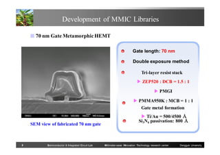
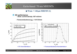
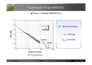
Download as PDF, PPTX

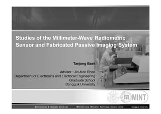
![GaAs-based 70 nm MHEMTs
■ fT
comparison of HEMTs
[1] Y. Yamashita et al., IEEE Electron Device Letters,
vol. 23, no. 10, pp. 573-575, 2002.
[2] K. Shinohara et al., IEEE Electron Device Letters,
vol. 25, no. 5, pp. 241-243, 2004.
[3] T. Suemitsu et al., IEEE Trans. on Electron Devices,
[1]
vol. 49, no. 10, pp. 1694-1700, 2002.
[2]
[4] K. Shinohara et al., IEEE Electron Device Letters,
vol. 22, no. 11, pp. 507-509, 2001.
This
work
[4]
[5] K. Shinohara et al., IEEE MTT-S Digest,
vol. 3, pp. 2159-2162, 2001.
[6] S. Bollaert et al., IEE Electronics Letters,
vol. 38, no. 8, pp. 389-391, 2002.
[3]
[5]
[8]
[6]
[7] T. Parenty et al., Indium Phosphide and
[9]
[7]
[10]
Related Materials, pp. 626-629, 2001.
[8] A. Leuther et al., Indium Phosphide and
Related Materials, pp. 215-218, 2003.
[9] H. Wang et al., IEEE IEDM Digest,
pp. 239-242, 1993.
[10] Y. C. Lien et al., IEEE Electron Device Letters,
vol. 25, no. 6, pp. 348-350, 2004.
This work: Sung Chan Kim et al.,
IEEE Electron Device Letters,
vol. 27, no. 1, pp. 28-30, 2006.
11
Semiconductor & Integrated Circuit Lab
Millimeter-wave INnovation Technology research center
Dongguk University](https://image.slidesharecdn.com/20130723researchaccomplishmentud-131121200044-phpapp01/85/20130723-research-accomplishment_ud-12-320.jpg)
![DAML Characteristic
■ Comparison of transmission lines
[1] K. Nishikawa et al., IEEE MTT-S Digest, vol. 3,
2001, pp. 1881-1884.
[2] G.E. Ponchak et al., IEEE Trans. Components,
Packaging, and Manufacturing Technology-B,
vol. 21, no. 2, pp. 171-176, 1998.
[3] Suidong Yang et al., IEEE Trans. Microwave
Theory and Techniques,
vol. 46, no. 5, pp. 623-631, 1998.
[4] Y.C. Shih et al., Microwave Journal,
pp. 95-105, 1991.
[5] Youngwoo Kwon et al., IEEE Microwave
and Wireless Components Letters,
vol. 11, no. 2, pp. 59-61, 2001.
[6] S.V. Robertson et al., IEEE Trans. Microwave
Theory and Techniques,
vol. 46, no. 11, 1998, pp. 1845-1849, 1998.
This work: H. S. Lee et al.,
IEE Electronics Letters,
vol. 39, no. 25, pp. 1827-1828, 2003.
This work: Sung-Chan Kim et al., IEEE Microwave
and Wireless Components Letters,
vol. 15, no. 10, pp. 652-654, 2005.
21
Semiconductor & Integrated Circuit Lab
Millimeter-wave INnovation Technology research center
Dongguk University](https://image.slidesharecdn.com/20130723researchaccomplishmentud-131121200044-phpapp01/85/20130723-research-accomplishment_ud-22-320.jpg)
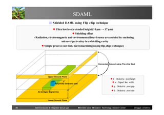
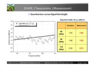
![SDAML Characteristic
■ Comparison of original DAML
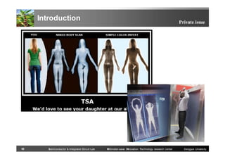
4.0
DAML (h = 10 m)
DAML (h = 17 m )
SDAML (h = 17 m)
60
(GHz)
94
(GHz)
120
(GHz)
DAML
(10 µm)
1.87
2.56
3.1
DAML
(17 µm)
1.27
1.89
2.42
SDAML
(17 µm)
3.5
1.07
1.41
1.67
Insertion loss [dB/cm]
3.0
2.5
2.0
1.5
1.0
0.5
0.0
0
20
40
60
80
100
120
140
Frequency [GHz]
25
Semiconductor & Integrated Circuit Lab
Millimeter-wave INnovation Technology research center
Dongguk University](https://image.slidesharecdn.com/20130723researchaccomplishmentud-131121200044-phpapp01/85/20130723-research-accomplishment_ud-26-320.jpg)
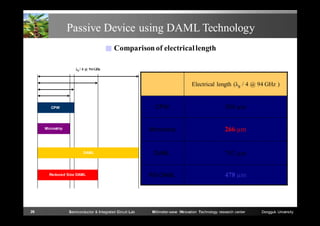
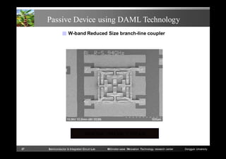
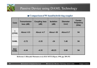
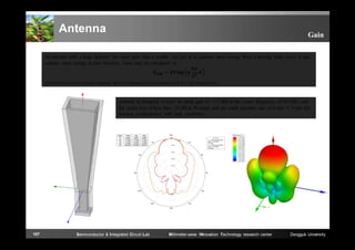
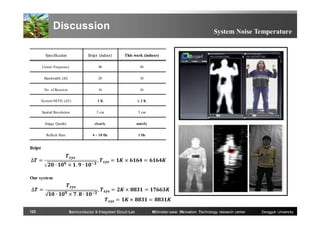
![Passive Device using DAML Technology
■ Measurement result of W-band reduced ring hybrid coupler
0
0
-10
S-parameter [dB]
S-parameter [dB]
-20
-30
-40
-50
S21Thru
S31coupling
S23Isolation
-60
75
80
85
-10
-20
-30
S11
S22
S33
-40
90
95
100
105
Frequency [GHz]
Insertion loss
110
70
75
80
85
90
95
100
105
115
Frequency [GHz]
Return loss
Coupling loss: 4.35 dB
Isolation: -48.23 dB
Transmission loss: 4.44 dB
35
110
Return loss: below -25 dB (all port)
Semiconductor & Integrated Circuit Lab
Millimeter-wave INnovation Technology research center
Dongguk University](https://image.slidesharecdn.com/20130723researchaccomplishmentud-131121200044-phpapp01/85/20130723-research-accomplishment_ud-36-320.jpg)
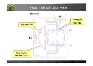
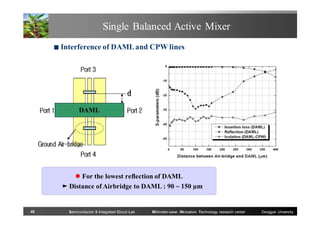
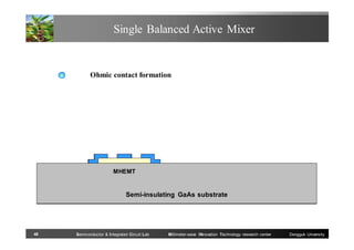
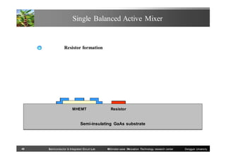
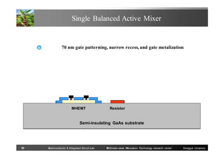
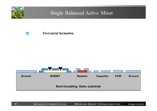
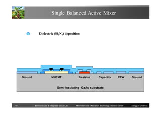
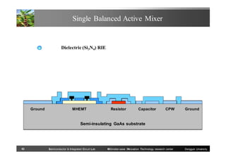
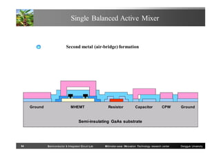
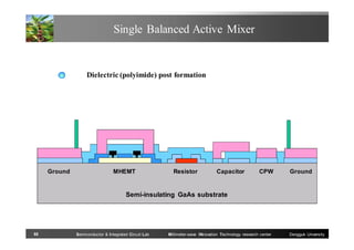
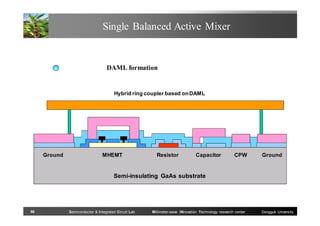
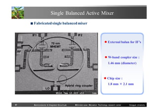
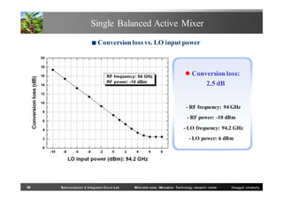
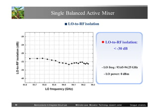
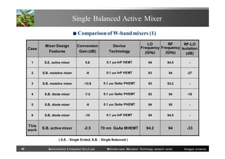
![Single Balanced Active Mixer
■
Comparison of W-band mixers (2)
Single balanced active mixer:
Low conversion loss: high-performance 70 nm MHEMTs
High isolation: hybrid ring coupler based on DAML
- References
[1] Robinder S. Virk et al., IEEE MTT-S Digest, 1997, pp. 435-438.
[2] A. R. Barnes et al., IEEE MTT-S Digest, 2002, pp. 1867-1870.
[3] K. W. Chang et al., IEEE Microwave and Guided Wave Letters, vol. 4, no. 9, pp. 301-302, 1994.
[4] K. W. Chang et al., IEEE Transactions on Microwave Theory and Techniques, vol. 39, no. 12, pp. 1972-1979, 1991.
[5] K. W. Chang et al., Proc. IEEE Microwave and Millimeter-wave Monolithic Circuits Symposium, 1993, pp. 41-44.
[6] Robinder S. Virk et al., IEEE MTT-S Digest, 1997, pp. 435-438.
This work: Sung Chan Kim et al., IEEE Electron Device Letters, vol. 27, no. 1, pp. 28-30, 2006.
61
Semiconductor & Integrated Circuit Lab
Millimeter-wave INnovation Technology research center
Dongguk University](https://image.slidesharecdn.com/20130723researchaccomplishmentud-131121200044-phpapp01/85/20130723-research-accomplishment_ud-62-320.jpg)


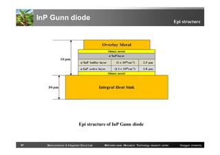
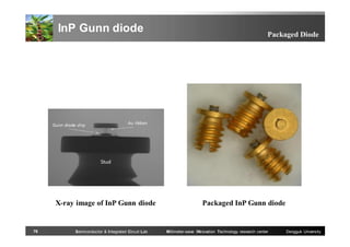
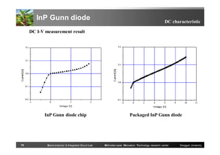
![InP Gunn diode
RF characteristic
Measurement results of packaged InP Gunn diode
Chip number
Voltage [V]
Current [mA]
Oscillation frequency [GHz]
Output Power [dBm]
1
12.4
299
94
17.8
2
11.7
260
93.98
16
3
9.7
299
94.25
15.6
4
10.9
349
93.9
16.6
5
9.3
349
93.8
16.4
Oscillation characteristics of fabricated InP Gunn diode
80
Semiconductor & Integrated Circuit Lab
Millimeter-wave INnovation Technology research center
Dongguk University](https://image.slidesharecdn.com/20130723researchaccomplishmentud-131121200044-phpapp01/85/20130723-research-accomplishment_ud-81-320.jpg)

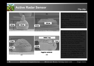
![Active Radar Sensor
RF Characteristic
0
S-parameter [dB]
-5
-10
-15
-20
-25
-30
Insertion loss
Return loss
-35
75
80
85
90
95
100
105
110
115
Frequency [dB]
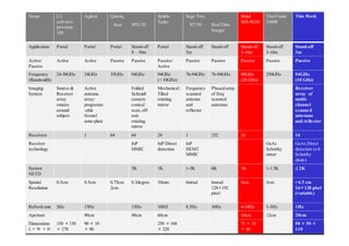
Reference
Bump material
Bonding condition
Loss/frequency
[1]
Au
350℃, 20 g/pillar
0.2 dB/77 GHz
[2]
Au
275℃, 230 N/mm2
0.2 dB/NA
This work
Au / Ag epoxy
110℃, 30g/bump
0.205 dB/94 GHz
[1] Aoki, S.; Someta, H.; Yokokawa, S.; Ono, K.; Hirose, T.; Ohashi, Y.;, “A flip chip bonding technology using gold pillars for
millimeter-wave applications,” in Proc. IEEE MTT-S Int. Microw. Symp. Dig. 1997, vol. 2, pp. 731-734, 1997.
[2] Heinrich, W.; Jentzsch, A.; Richter, H.;, “Flip-chip interconnects for frequencies up to W band,” Electron. Lett., vol. 37, issue 3, pp.
180-181, 2001.
90
Semiconductor & Integrated Circuit Lab
Millimeter-wave INnovation Technology research center
Dongguk University](https://image.slidesharecdn.com/20130723researchaccomplishmentud-131121200044-phpapp01/85/20130723-research-accomplishment_ud-91-320.jpg)
![Active Radar Sensor
Shear test
The shear tests were performed using a model 4000 series shear test machine from DageTM , widely used
to measure the interconnection strength between the MMIC chip and the sapphire substrate. The speed of
the shear blade was 300 μm/s, with the tip located at 40 μm above the surface of the sapphire substrate.
The flip-chip bonded die, which used proposed low-temperature flip-chip bonding method and 20 bumps
of 100 μm diameter, was separated at a force of 900 g.
Bonding temperature
Die shear strength [mg/ ㎛2]
100℃
1.55
150℃
2.19
200℃
4.38
ACP
220℃
1.05
ACF
220℃
1.07
[3]
CuSn
260℃
2.17
This work
Au/Ag epoxy
110℃
5.73
Reference
[1]
Bump material
Indium
[2]
[1] Kun-Mo Chu, Jung-Sub Lee, Han Seo Cho, Hyo-Hoon Park, Duk Young Jeon, “A fluxless flip-chip bonding for VCSEL arrays using
silver-coated indium solder bumps,” IEEE Trans. Electronics Packag. Manuf., vol. 27, no. 4, pp. 246-253, 2004.
[2] Tan Ai Min, Sharon Pei-Siang Lim and Charles Lee, “Development of solder replacement flip chip using anisotropic conductive
adhesives,” in Proc. 5 th Electron. Packag. Tech. Conf. 2003, pp. 390-396, 2003.
[3] Katsuyuki Sakuma, Jun Mizuno, Noriyasu Nagai, Naoko Unami, and Shuichi Shoji, “Effects of Vacuum Ultraviolet Surface
Treatment on the Bonding Interconnections for Flip Chip and 3-D Integration.” IEEE Trans. Electronics Packag. Manuf., vol. 33, no. 3,
pp. 212-220, 2010.
92
Semiconductor & Integrated Circuit Lab
Millimeter-wave INnovation Technology research center
Dongguk University](https://image.slidesharecdn.com/20130723researchaccomplishmentud-131121200044-phpapp01/85/20130723-research-accomplishment_ud-93-320.jpg)


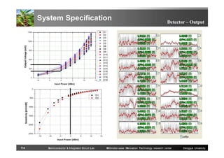
![LNA
LNA module – 4-stage
80
60
S11
S-Parameter [dB]
40
S21
S12
20
S22
0
-20
-40
-60
-80
80
85
90
95
Frequency [GHz]
100
105
110
4-stage LNA module measured characteristics
Average linear gain: 65.8 dB @ 81 ~ 102 GHz
68.2 dB @ 94 GHz
112
Semiconductor & Integrated Circuit Lab
Millimeter-wave INnovation Technology research center
Dongguk University](https://image.slidesharecdn.com/20130723researchaccomplishmentud-131121200044-phpapp01/85/20130723-research-accomplishment_ud-113-320.jpg)


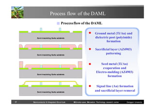
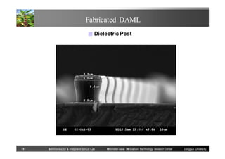
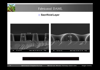
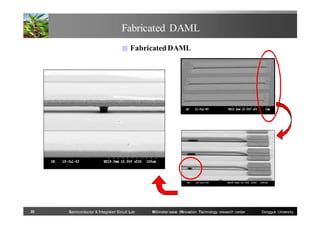
This document describes research in millimeter-wave integrated circuits conducted by Taejong Baek at Dongguk University. The research focuses on developing monolithic integrated circuits for millimeter-wave applications using semiconductor technologies like metamorphic HEMTs with 70nm gate lengths. Key accomplishments include fabricating 70nm gate length MHEMTs with an fT of 330GHz and fmax of 425GHz, as well as developing dielectric-supported air-gap microstrip lines (DAML) to reduce transmission line losses in millimeter-wave integrated circuits. The DAML fabrication process uses only photolithography and low-temperature processes for compatibility with standard MMIC fabrication.