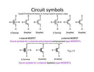
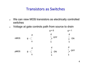
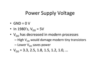
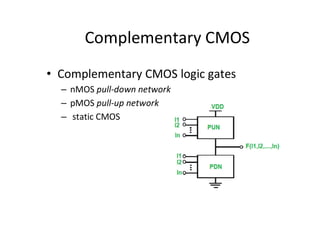
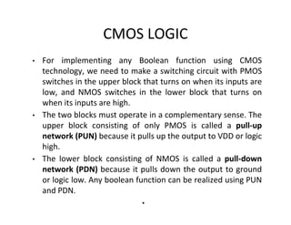
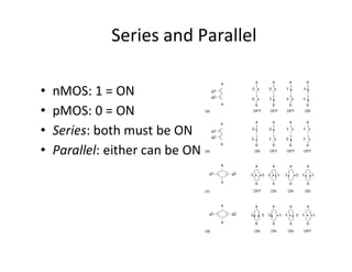
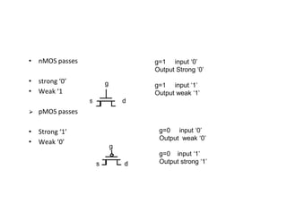
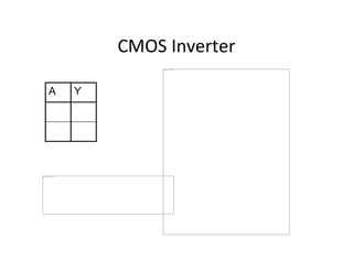
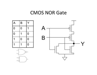
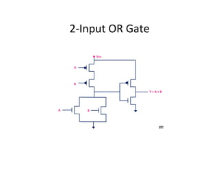
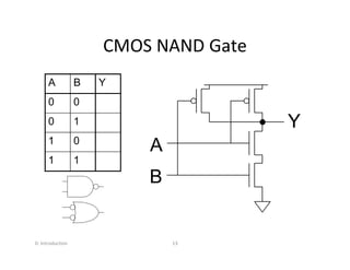
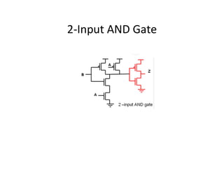
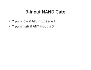
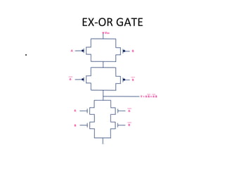
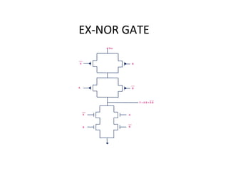
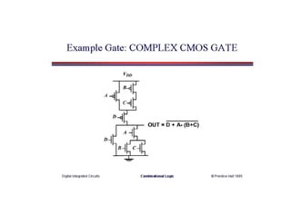
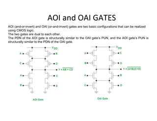
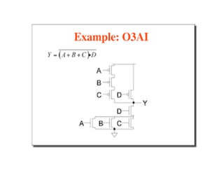
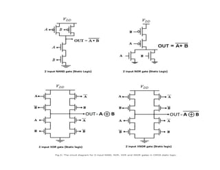
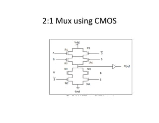
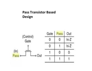
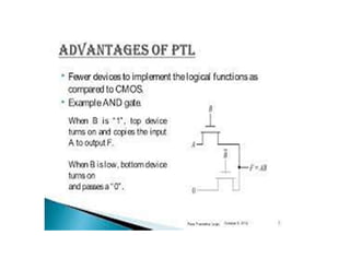
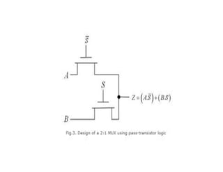
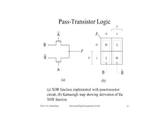
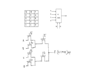
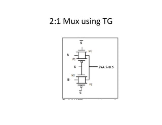
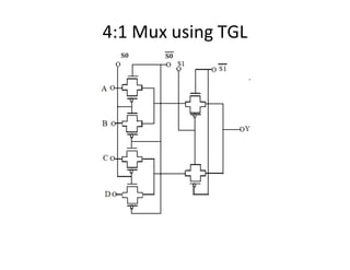
VLSI DESIGN
Circuit symbols
Circuit symbols for n-channel and p-channel enhancement-type MOSFETs
Circuit symbols for n-channel depletion-type MOSFETs
4
Transistors as Switches
❑ We can view MOS transistors as electrically controlled
switches
❑ Voltage at gate controls path from source to drain
Power Supply Voltage
• GND = 0 V
• In 1980’s, VDD = 5V
• VDD has decreased in modern processes
– High VDD would damage modern tiny transistors
– Lower VDD saves power
• VDD = 3.3, 2.5, 1.8, 1.5, 1.2, 1.0, …
Complementary CMOS
• Complementary CMOS logic gates
– nMOS pull-down network
– pMOS pull-up network
– static CMOS
CMOS LOGIC
• For implementing any Boolean function using CMOS
technology, we need to make a switching circuit with PMOS
switches in the upper block that turns on when its inputs are
low, and NMOS switches in the lower block that turns on
when its inputs are high.
• The two blocks must operate in a complementary sense. The
upper block consisting of only PMOS is called a pull-up
network (PUN) because it pulls up the output to VDD or logic
high.
• The lower block consisting of NMOS is called a pull-down
network (PDN) because it pulls down the output to ground
or logic low. Any boolean function can be realized using PUN
and PDN.
•
Series and Parallel
• nMOS: 1 = ON
• pMOS: 0 = ON
• Series: both must be ON
• Parallel: either can be ON
• nMOS passes
• strong ‘0’
• Weak ‘1
⮚ pMOS passes
• Strong ‘1’
• Weak ‘0’
g
s d
g
s d
g=1 input ‘0’
Output Strong ‘0’
g=1 input ‘1’
Output weak ‘1’
g=0 input ‘0’
Output weak ‘0’
g=0 input ‘1’
Output strong ‘1’
0
This image cannot currently be displayed.
CMOS Inverter
A Y
0 1
1 0
This image cannot currently be displayed.
OFF
ON
1
ON
OFF
CMOS NOR Gate
A B Y
0 0 1
0 1 0
1 0 0
1 1 0
2-Input OR Gate
0: Introduction 13
CMOS NAND Gate
A B Y
0 0 1
0 1 1
1 0 1
1 1 0
OFF
OFF
ON
ON
1
1
OFF
ON
OFF
ON
0
1
ON
OFF
ON
OFF
1
0
ON
ON
OFF
OFF
0
0
2-Input AND Gate
3-input NAND Gate
• Y pulls low if ALL inputs are 1
• Y pulls high if ANY input is 0
EX-OR GATE
•
EX-NOR GATE
AOI and OAI GATES
AOI (and-or-invert) and OAI (or-and-invert) gates are two basic configurations that can be realized
using CMOS logic.
The two gates are dual to each other.
The PDN of the AOI gate is structurally similar to the OAI gate’s PUN, and the AOI gate’s PUN is
structurally similar to the PDN of the OAI gate.
2:1 Mux using CMOS
Other design Styles
Other design Styles
1. Pass Transistor Based Design (PTL)
2. Transmission gate Based Design (TG)
Pass Transistor Based
Design
2:1 Mux using TG
4:1 Mux using TGL
Comparison Study
• Power consumption by multiplexer designed using
Transmission gate as well as CMOS is remarkably low as
compared to that designed by Pass Transistor Logic, although
the least power is consumed by 2:1 multiplexer
implemented using TGL.
• There is a huge difference in number of transistors used to
design these circuits.
• Since multiplexer implemented by PTL utilizes minimum
number of transistors, i.e., 2 therefore it is the area efficient
logic circuit for 2:1 MUX but its performance is low as its
output is somewhat distorted.
• CMOS uses large number of components but its performance
is high and its switching time is minimum therefore its delay
is the minimum as compared to those of TGL and PTL
circuits.

2. Unit1-CMOS PTL TGL Logic.pdf

  • 1.
  • 3.
    Circuit symbols Circuit symbolsfor n-channel and p-channel enhancement-type MOSFETs Circuit symbols for n-channel depletion-type MOSFETs
  • 4.
    4 Transistors as Switches ❑We can view MOS transistors as electrically controlled switches ❑ Voltage at gate controls path from source to drain
  • 5.
    Power Supply Voltage •GND = 0 V • In 1980’s, VDD = 5V • VDD has decreased in modern processes – High VDD would damage modern tiny transistors – Lower VDD saves power • VDD = 3.3, 2.5, 1.8, 1.5, 1.2, 1.0, …
  • 6.
    Complementary CMOS • ComplementaryCMOS logic gates – nMOS pull-down network – pMOS pull-up network – static CMOS
  • 7.
    CMOS LOGIC • Forimplementing any Boolean function using CMOS technology, we need to make a switching circuit with PMOS switches in the upper block that turns on when its inputs are low, and NMOS switches in the lower block that turns on when its inputs are high. • The two blocks must operate in a complementary sense. The upper block consisting of only PMOS is called a pull-up network (PUN) because it pulls up the output to VDD or logic high. • The lower block consisting of NMOS is called a pull-down network (PDN) because it pulls down the output to ground or logic low. Any boolean function can be realized using PUN and PDN. •
  • 8.
    Series and Parallel •nMOS: 1 = ON • pMOS: 0 = ON • Series: both must be ON • Parallel: either can be ON
  • 9.
    • nMOS passes •strong ‘0’ • Weak ‘1 ⮚ pMOS passes • Strong ‘1’ • Weak ‘0’ g s d g s d g=1 input ‘0’ Output Strong ‘0’ g=1 input ‘1’ Output weak ‘1’ g=0 input ‘0’ Output weak ‘0’ g=0 input ‘1’ Output strong ‘1’
  • 10.
    0 This image cannotcurrently be displayed. CMOS Inverter A Y 0 1 1 0 This image cannot currently be displayed. OFF ON 1 ON OFF
  • 11.
    CMOS NOR Gate AB Y 0 0 1 0 1 0 1 0 0 1 1 0
  • 12.
  • 13.
    0: Introduction 13 CMOSNAND Gate A B Y 0 0 1 0 1 1 1 0 1 1 1 0 OFF OFF ON ON 1 1 OFF ON OFF ON 0 1 ON OFF ON OFF 1 0 ON ON OFF OFF 0 0
  • 14.
  • 15.
    3-input NAND Gate •Y pulls low if ALL inputs are 1 • Y pulls high if ANY input is 0
  • 16.
  • 17.
  • 19.
    AOI and OAIGATES AOI (and-or-invert) and OAI (or-and-invert) gates are two basic configurations that can be realized using CMOS logic. The two gates are dual to each other. The PDN of the AOI gate is structurally similar to the OAI gate’s PUN, and the AOI gate’s PUN is structurally similar to the PDN of the OAI gate.
  • 22.
  • 24.
  • 25.
    Other design Styles 1.Pass Transistor Based Design (PTL) 2. Transmission gate Based Design (TG)
  • 26.
  • 31.
  • 32.
  • 33.
    Comparison Study • Powerconsumption by multiplexer designed using Transmission gate as well as CMOS is remarkably low as compared to that designed by Pass Transistor Logic, although the least power is consumed by 2:1 multiplexer implemented using TGL. • There is a huge difference in number of transistors used to design these circuits. • Since multiplexer implemented by PTL utilizes minimum number of transistors, i.e., 2 therefore it is the area efficient logic circuit for 2:1 MUX but its performance is low as its output is somewhat distorted. • CMOS uses large number of components but its performance is high and its switching time is minimum therefore its delay is the minimum as compared to those of TGL and PTL circuits.