SlideShare a Scribd company logo
1 of 17
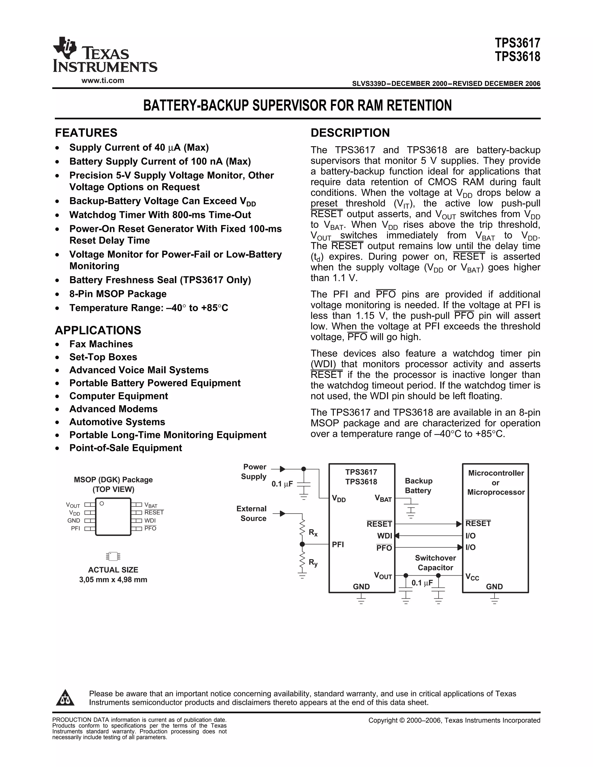
Download to read offline
www.ti.com
FEATURES DESCRIPTION
APPLICATIONS
VDD VBAT
PFI
Backup
Battery
RESET
WDI
PFO
VOUT
GND
Rx
Ry
External
Source
0.1 µF
Power
Supply
GND
RESET
I/O
I/O
VCC
Switchover
Capacitor
0.1 µF
TPS3617
TPS3618
Microcontroller
or
Microprocessor
ACTUAL SIZE
3,05 mm x 4,98 mm
VBAT
RESET
WDI
PFO
VOUT
VDD
GND
PFI
MSOP (DGK) Package
(TOP VIEW)
TPS3617
TPS3618
SLVS339D–DECEMBER 2000–REVISED DECEMBER 2006
BATTERY-BACKUP SUPERVISOR FOR RAM RETENTION
• Supply Current of 40 µA (Max) The TPS3617 and TPS3618 are battery-backup
supervisors that monitor 5 V supplies. They provide• Battery Supply Current of 100 nA (Max)
a battery-backup function ideal for applications that• Precision 5-V Supply Voltage Monitor, Other
require data retention of CMOS RAM during fault
Voltage Options on Request
conditions. When the voltage at VDD drops below a
• Backup-Battery Voltage Can Exceed VDD preset threshold (VIT), the active low push-pull
RESET output asserts, and VOUT switches from VDD• Watchdog Timer With 800-ms Time-Out
to VBAT. When VDD rises above the trip threshold,• Power-On Reset Generator With Fixed 100-ms
VOUT switches immediately from VBAT to VDD.
Reset Delay Time
The RESET output remains low until the delay time
• Voltage Monitor for Power-Fail or Low-Battery (td) expires. During power on, RESET is asserted
Monitoring when the supply voltage (VDD or VBAT) goes higher
than 1.1 V.• Battery Freshness Seal (TPS3617 Only)
• 8-Pin MSOP Package The PFI and PFO pins are provided if additional
voltage monitoring is needed. If the voltage at PFI is• Temperature Range: –40° to +85°C
less than 1.15 V, the push-pull PFO pin will assert
low. When the voltage at PFI exceeds the threshold
voltage, PFO will go high.
• Fax Machines
These devices also feature a watchdog timer pin• Set-Top Boxes
(WDI) that monitors processor activity and asserts
• Advanced Voice Mail Systems RESET if the the processor is inactive longer than
• Portable Battery Powered Equipment the watchdog timeout period. If the watchdog timer is
• Computer Equipment not used, the WDI pin should be left floating.
• Advanced Modems The TPS3617 and TPS3618 are available in an 8-pin
• Automotive Systems MSOP package and are characterized for operation
over a temperature range of –40°C to +85°C.• Portable Long-Time Monitoring Equipment
• Point-of-Sale Equipment
Please be aware that an important notice concerning availability, standard warranty, and use in critical applications of Texas
Instruments semiconductor products and disclaimers thereto appears at the end of this data sheet.
PRODUCTION DATA information is current as of publication date. Copyright © 2000–2006, Texas Instruments Incorporated
Products conform to specifications per the terms of the Texas
Instruments standard warranty. Production processing does not
necessarily include testing of all parameters.
www.ti.com
ABSOLUTE MAXIMUM RATINGS
DISSIPATION RATING TABLE
TPS3617
TPS3618
SLVS339D–DECEMBER 2000–REVISED DECEMBER 2006
This integrated circuit can be damaged by ESD. Texas Instruments recommends that all integrated circuits be handled with
appropriate precautions. Failure to observe proper handling and installation procedures can cause damage.
ESD damage can range from subtle performance degradation to complete device failure. Precision integrated circuits may be
more susceptible to damage because very small parametric changes could cause the device not to meet its published
specifications.
PACKAGE INFORMATION(1)
NOMINAL SPECIFIED
SUPPLY THRESHOLD TEMPERATURE PACKAGE ORDERING TRANSPORT MEDIA,
PRODUCT VOLTAGE VOLTAGE (VIT)(2) RANGE MARKING NUMBER QUANTITY
TPS3617-50DGK Tube, 80
TPS3617-50 ASD
TPS3617-50DGKR Tape and Reel, 2500
5V 4.55V –40°C to +125°C
TPS3618-50DGKT Tape and Reel, 250
TPS3618-50 ANK
TPS3618-50DGKR Tape and Reel, 2500
(1) For the most current package and ordering information, see the Package Option Addendum at the end of this data sheet, or refer to our
web site at www.ti.com.
(2) For other threshold votages, contact the local TI sales office for availability and lead time.
over operating free-air temperature (unless otherwise noted)(1)
TPS3617, TPS3618 UNIT
Input voltage range, VDD –0.3 to 7 V
Input voltage range, PFI pin –0.3 to (VDD + 0.3) V
WDI pin –0.3 to (VDD + 0.3) V
Continuous output current at VOUT, IO 400 mA
All other pins, IO ±10 mA
Operating junction temperature range, TJ
(2) –40 to +85 °C
Storage temperature range, TSTG –65 to +150 °C
Lead temperature soldering 1,6 mm (1/16 inch) from case for 10 seconds +260 °C
Continuous total power dissipation See Dissipation Rating Table
(1) Stresses beyond those listed under Absolute Maximum Ratings may cause permanent damage to the device. These are stress ratings
only, and functional operation of the device at these or any other conditions beyond those indicated under Recommended Operating
Conditions is not implied. Exposure to absolute-maximum-rated conditions for extended periods may affect device reliability.
(2) Due to the low dissipated power in this device, it is assumed that TJ = TA.
TA ≤ +25°C DERATING FACTOR TA = +70°C TA = +85°C
PACKAGE POWER RATING ABOVE TA = +25°C POWER RATING POWER RATING
DGK 470 mW 3.76 mW/°C 301 mW 241 mW
2 Submit Documentation Feedback
www.ti.com
ELECTRICAL CHARACTERISTICS
TPS3617
TPS3618
SLVS339D–DECEMBER 2000–REVISED DECEMBER 2006
1.65 V ≤ VDD≤ 5.5 V, RLRESET = 1 MΩ, CLRESET = 50 pF, over operating temperature range (TJ = –40°C to +85°C), unless
otherwise noted. Typical values are at TJ = +25°C.
PARAMETER TEST CONDITIONS MIN TYP MAX UNIT
VDD Input supply range 1.65 5.5 V
VOUT = VDD 40
IDD VDD supply current µA
VOUT = VBAT 40
VBAT Battery supply range 1.5 5.5 V
VOUT = VDD –0.1 0.1
IBAT VBAT supply current µ A
VOUT = VBAT 0.5
Slew rate at VDD or VBAT 1 V/µs
VI Input volrage, any input 0 VDD + 0.3 V
VDD = 1.8 V, IOH = –400 µA VDD – 0.2
RESET VDD = 3.3 V, IOH = –2 mA,
VDD – 0.4
VDD = 5 V, IOH = –3 mA
VOH High-level output voltage V
VDD = 1.8 V, IOH = –20 µA VDD – 0.3
PFO VDD = 3.3 V, IOH = –80 µA,
VDD – 0.4
VDD = 5 V, IOH = –120 µA
VDD = 1.8 V, IOL = 400 µA 0.2
VOL Low-level output voltage RESET PFO VVDD = 3.3 V, IOL = 2 mA,
0.4
VDD = 5 V, IOL = 3 mA
VBAT > 1.1 V, or VDD > 1.1 V,
VRES Power-up reset voltage (1) 0.4 V
IOL = 20 µA
IO = 8.5 mA,VDD = 1.8 V, VBAT = 0 V VDD – 0.050
Normal mode IO = 125 mA,VDD = 3.3 V, VBAT = 0 V VDD – 0.150
VOUT IO = 200 mA,VDD = 5 V, VBAT = 0 V VDD – 0.200 V
IO = 0.5 mA,VBAT = 1.5 V, VDD = 0 V VBAT – 0.200
Battery-backup mode
IO = 7.5 mA,VBAT = 3.3 V, VDD = 0 V VBAT – 0.113
VDD to VOUT on-resistance VDD = 5 V 0.6 1
RDS(on) Ω
VBAT to VOUT on-resistance VBAT = 3.3 V 8 15
IO Continuous output current at VOUT 300 mA
VIT TPS3617-50 4.46 4.55 VNegative-going input
TA = –40°C to +85°C
threshold voltage (2)
VPFI PFI 1.13 1.15 1.17 V
1.65 V < VIT < 2.5 V 20
VIT hysteresis 2.5 V < VIT < 3.5 V 40
VHYS 3.5 V < VIT < 5.5 V 60 mV
PFI hysteresis 12
VBSW hysteresis (3) VDD = 1.8 V 55
VIH WDI high-level input voltage 0.7 x VDD
VIL WDI low-level input voltage 0.3 x VDD
IIH WDI high-level input current (4) WDI = VDD = 5 V 150 µA
IIL WDI low-level input current (4) WDI = 0 V, VDD = 5 V –150 µA
WDI input transition rise and fall rate, ∆t/∆V 100 ns/V
II PFI input current PFI voltage < VDD –25 25 nA
PFO = 0 V, VDD = 1.8 V –0.3
IOS PFO short-circuit current PFO = 0 V, VDD = 3.3 V –1.1 mA
PFO = 0 V, VDD = 5 V –2.4
(1) The lowest supply voltage at which RESET becomes active. tr, VDD ≥ 15 µs/V.
(2) To ensure the best stability of the threshold voltage, a bypass capacitor (ceramic, 0.1 µF) should be placed near the supply terminals.
(3) For VDD < 1.6 V, VOUT switches to VBAT regardless of VBAT.
(4) For details on how to optimize current consumption when using WDI, refer to the Watchdog section of this data sheet.
3Submit Documentation Feedback
www.ti.com
VIT
VBAT
VDD
VOUT
RESET
td
t
t
t
td
TPS3617
TPS3618
SLVS339D–DECEMBER 2000–REVISED DECEMBER 2006
ELECTRICAL CHARACTERISTICS (continued)
1.65 V ≤ VDD≤ 5.5 V, RLRESET = 1 MΩ, CLRESET = 50 pF, over operating temperature range (TJ = –40°C to +85°C), unless
otherwise noted. Typical values are at TJ = +25°C.
PARAMETER TEST CONDITIONS MIN TYP MAX UNIT
Ci Input capacitance, any input VI = 0 V to 5 V 5 pF
VDD VIH = VIT + 0.2 V, VIL = VIT– 0.2 V 6 µs
tw Pulse Width VDD > VIT + 0.2 V, VIL = 0.3 x VDD,
WDI 100 ns
VIH = 0.7 x VDD
td VDD ≥ VIT + 0.2 V,
Delay time 60 100 140 ms
See timing diagram
t(tout) VDD > VIT + 0.2 V,
Watchdog time-out 0.48 0.8 1.12 s
See timing diagram
VIL = VIT– 0.2 V,
VDD to RESET 2 5
VIH = VIT + 0.2 VPropagation (delay) time,
tPHL µs
high-to-low-level output VIL = VPFI– 0.2 V,
PFI to PFO 3 5
VIH = VPFI + 0.2 V
Transition time VDD to VBAT 3 µs
TIMING DIAGRAM
Table 1. FUNCTION TABLE
VDD > VIT VDD > VBAT VOUT RESET
0 0 VBAT 0
0 1 VDD 0
1 0 VDD 1
1 1 VDD 1
4 Submit Documentation Feedback
www.ti.com
Switch
Control_
+
RESET
Logic
+
Timer_
+
Reference
Voltage
or 1.15 V
VOUT
RESET
VBAT
VDD
PFI
TPS3617
GND
Watchdog
Logic
+
Control
Oscillator
PFO
+
−
Transition
Detector
WDI
40 kΩ
TPS3618
TPS3617
TPS3618
SLVS339D–DECEMBER 2000–REVISED DECEMBER 2006
Table 2. PFO FUNCTION
TABLE
PFI > VPFI PFO
0 0
1 1
CONDITION: VDD > VDD(MIN)
Table 3. TERMINAL FUNCTIONS
TERMINAL
NAME NO. I/O DESCRIPTION
GND 3 I Ground
PFI 4 I Power-fail comparator input
PFO 5 O Power-fail comparator output; asserts low when PFI < 1.15 V
RESET 7 O Active-low push-pull reset output
VBAT 8 I Backup-battery input
VDD 2 I Input supply voltage
VOUT 1 O Supply output
WDI 6 I Watchdog input. Should be left floating if not used.
FUNCTIONAL BLOCK DIAGRAM
5Submit Documentation Feedback
www.ti.com
TYPICAL CHARACTERISTICS
TABLE OF GRAPHS
5
7.5
10
12.5
15
17.5
20
2.5 4.5 6.5 8.5 10.5 12.5 14.5
−StaticDrain-SourceOn-StateResistance−
IO − Output Current − mA
rDS(on)Ω
TA = 85°C
VBAT = 3.3 V
TA = 25°C
TA = 0°C
TA = −40°C
500
600
700
800
900
1000
50 75 100 125 150 175 200
TA = 85°C
TA = 25°C
TA = 0°C
TA = −40°C
−StaticDrain-SourceOn-StateResistance−m
VDD = 3.3 V
VBAT = GND
IO − Output Current − mA
rDS(on)Ω
TPS3617
TPS3618
SLVS339D–DECEMBER 2000–REVISED DECEMBER 2006
FIGURE
Static drain-source on-state resistance (VDD to VOUT) vs Output current 3
rDS(on)
Static drain-source on-state resistance (VBAT to VOUT) vs Output current 4
IDD Supply current vs Supply voltage 5
VIT Input threshold voltage at RESET vs Free-air temperature 6
High-level output voltage at RESET 7, 8
VOH vs High-level output current
High-level output voltage at PFO 9, 10
VOL Low-level output voltage at RESET vs Low-level output current 11, 12
Minimum pulse duration at VDD vs Threshold voltage overdrive at VDD 13
Minimum pulse duration at PFI vs Threshold voltage overdrive at PFI 14
STATIC DRAIN-SOURCE ON-STATE RESISTANCE STATIC DRAIN-SOURCE ON-STATE RESISTANCE
(VDD to VOUT) (VBAT to VOUT)
vs vs
OUTPUT CURRENT OUTPUT CURRENT
Figure 1. Figure 2.
6 Submit Documentation Feedback
www.ti.com
0.995
0.996
0.997
0.998
0.999
1
1.001
−40 −30 −20 −10 0 10 20 30 40 50 60 70 80
TA − Free-Air Temperature − °C
−InputThresholdVoltageatRESET−VVIT
0
5
10
15
20
25
30
0 1 2 3 4 5 6
TA = −40°C
TA = 25°C
TA = 85°C
TA = 0°C
−SupplyCurrent−IDDAµ
VDD − Supply Voltage − V
VBAT Mode
VBAT = 2.6 V
VDD Mode
VBAT = GNDor
0
1
2
3
4
5
6
−35 −30 −25 −20 −15 −10 −5 0
TA = −40°C
TA = 85°C
TA = 0°C
TA = 25°C
−High-LevelOutputVoltageatRESET−VVOH
IOH − High-Level Output Current − mA
VDD = 5 V
VBAT = GND
TPS3617
TPS3618
SLVS339D–DECEMBER 2000–REVISED DECEMBER 2006
SUPPLY CURRENT INPUT THRESHOLD VOLTAGE AT RESET
vs vs
SUPPLE VOLTAGE FREE-AIR TEMPERATURE
Figure 3. Figure 4.
HIGH-LEVEL OUTPUT VOLTAGE AT RESET
vs
HIGH-LEVEL OUTPUT CURRENT
Figure 5.
7Submit Documentation Feedback
www.ti.com
0
1
2
3
4
5
6
−2.5 −2 −1.5 −1 −0.5 0
TA = −40°C
TA = 25°C
TA = 85°C
TA = 0°C
−High-LevelOutputVoltageatPFO−VVOH
IOH − High-Level Output Current − mA
VDD = 5.5 V
PFI = 1.4 V
VBAT = GND
4.5
4.6
4.7
4.8
4.9
5
5.1
−5 −4.5 −4 −3.5 −3 −2.5 −2 −1.5 −1 −0.5 0
TA = −40°C
TA = 25°C
TA = 85°C
TA = 0°C
IOH − High-Level Output Current − mA
VDD = 5 V
VBAT = GND
Expanded View
−High-LevelOutputVoltageatRESET−VVOH
0
0.5
1
1.5
2
2.5
3
3.5
0 5 10 15 20 25
TA = 25°C
TA = 85°C
TA = 0°C
TA = −40°C
−Low-LevelOutputVoltageatRESET−VVOL
IOL − Low-Level Output Current − mA
VDD = 3.3 V
VBAT = GND
5.10
5.15
5.20
5.25
5.30
5.35
5.40
5.45
5.50
5.55
−200 −180−160−140 −120−100 −80 −60 −40 −20 0
TA = −40°C
TA = 25°C
TA = 85°C
TA = 0°C
IOH − High-Level Output Current − µA
VDD = 5.5 V
PFI = 1.4 V
VBAT = GND
Expanded View
−High-LevelOutputVoltageatPFO−VVOH
TPS3617
TPS3618
SLVS339D–DECEMBER 2000–REVISED DECEMBER 2006
HIGH-LEVEL OUTPUT VOLTAGE AT RESET HIGH-LEVEL OUTPUT VOLTAGE AT PFO
vs vs
HIGH-LEVEL OUTPUT CURRENT HIGH-LEVEL OUTPUT CURRENT
Figure 6. Figure 7.
HIGH-LEVEL OUTPUT VOLTAGE AT PFO LOW-LEVEL OUTPUT VOLTAGE AT RESET
vs vs
HIGH-LEVEL OUTPUT CURRENT LOW-LEVEL OUTPUT CURRENT
Figure 8. Figure 9.
8 Submit Documentation Feedback
www.ti.com
0
100
200
300
400
500
0 1 2 3 4 5
TA = −40°C
TA = 25°C
TA = 85°C
TA = 0°C
−Low-LevelOutputVoltageatRESET−mVVOL
IOL − Low-Level Output Current − mA
VDD = 3.3 V
VBAT = GND
Expanded View
0
1
2
3
4
5
6
7
8
9
10
0 0.1 0.2 0.3 0.4 0.5 0.6 0.7 0.8 0.9
MinimumPulseDurationat−VDD Threshold Voltage Overdrive at VDD − V
1
sµ
0.6
1
1.4
1.8
2.2
2.6
3
3.4
3.8
4.2
4.6
5
0 0.1 0.2 0.3 0.4 0.5 0.6 0.7 0.8 0.9 1
MinimumPulseDurationatPFI−
Threshold Voltage Overdrive at PFI − V
VDD = 1.65 V
sµ
TPS3617
TPS3618
SLVS339D–DECEMBER 2000–REVISED DECEMBER 2006
LOW-LEVEL OUTPUT VOLTAGE AT RESET MINIMUM PULSE DURATION AT VDD
vs vs
LOW-LEVEL OUTPUT CURRENT THRESHOLD VOLTAGE OVERDRIVE AT VDD
Figure 10. Figure 11.
MINIMUM PULSE DURATION AT PFI
vs
THRESHOLD VOLTAGE OVERDRIVE AT PFI
Figure 12.
9Submit Documentation Feedback
www.ti.com
DETAILED DESCRIPTION
BATTERY FRESHNESS SEAL (TPS3617 Only)
POWER-FAIL COMPARATOR (PFI AND PFO)
WATCHDOG
VIT
WDI
RESET
td td
t(tout)
VOUT
td
Undefined
TPS3617
TPS3618
SLVS339D–DECEMBER 2000–REVISED DECEMBER 2006
The battery freshness seal of the TPS3617 family disconnects the backup battery from the internal circuitry until
it is needed. This ensures that the backup battery connected to VBAT should be fresh when the final product is
put to use. The following steps explain how to enable the freshness seal mode:
1. Connect VBAT (VBAT > VBAT(min)).
2. Ground PFO.
3. Connect PFI to VDD (PFI = VDD).
4. Connect VDD to power supply (VDD > VIT) and keep connected for 5 ms < t < 35 ms.
The battery freshness seal mode is disabled by the positive-going edge of RESET when VDD is applied.
An additional comparator monitors voltages other than the nominal supply voltage. The power-fail-input (PFI)
can be compared with an internal voltage reference of 1.15 V. If the input voltage falls below the power-fail
threshold (V(PFI)) of 1.15 V typical, the power-fail output (PFO) goes low. If it goes above V(PFI) plus about 12-mV
hysteresis, the output returns to high. By connecting two external resistors it is possible to supervise any
voltages above V(PFI). The sum of both resistors should be about 1 MΩ, to minimize power consumption and
also to ensure that the current in the PFI pin can be neglected compared with the current through the resistor
network. The tolerance of the external resistors should be not more than 1% to ensure minimal variation of the
sensed voltage. If the power-fail comparator is unused, connect PFI to ground and leave the PFO unconnected.
In a microprocessor- or DSP-based system, it is not only important to supervise the supply voltage, it is also
important to ensure correct program execution. The task of a watchdog is to ensure that the program is not
stalled in an indefinite loop. The microprocessor, microcontroller, or DSP has to toggle the watchdog input within
0.8 s typically, to avoid a timeout from occurring. Either a low-to-high or a high-to-low transition resets the
internal watchdog timer. If the input is unconnected, the watchdog is disabled and should be retriggered
internally. See Figure 13 for the watchdog timing diagram.
Figure 13. Watchdog Timing
10 Submit Documentation Feedback
www.ti.com
SAVING CURRENT WHILE USING THE WATCHDOG
BACKUP-BATTERY SWITCHOVER
VDD – Mode
VBAT – Mode
VBSW Hysteresis
VIT Hysteresis
VBAT – Backup-Battery Supply Voltage
–NormalSupplyVoltageVDD
Undefined
TPS3617
TPS3618
SLVS339D–DECEMBER 2000–REVISED DECEMBER 2006
DETAILED DESCRIPTION (continued)
The watchdog input is internally driven low during the first 7/8 of the watchdog time-out period, then momentarily
pulses high, resetting the watchdog counter. For minimum watchdog input current (minimum overall power
consumption), leave WDI low for the majority of the watchdog time-out period, pulsing it low-high-low once within
7/8 of the watchdog time-out period to reset the watchdog timer. If instead, WDI is externally driven high for the
majority of the time-out period, a current of e.g. 5.0 V/40 kΩ ≈ 125 µA can flow into WDI.
In case of a brownout or power failure, it may be necessary to preserve the contents of RAM. If a backup battery
is installed at VBAT, the device automatically switches the connected RAM to backup power when VDD fails. In
order to allow the backup battery (e.g., a 3.6-V lithium cell) to have a higher voltage than VDD, these supervisors
should not connect VBAT to VOUT when VBAT is greater than VDD. VBAT only connects to VOUT (through a 15-Ω
switch) when VDD falls below VIT and VBAT is greater than VDD. When VDD recovers, switchover is deferred either
until VDD crosses VBAT, or until VDD rises above the reset threshold VIT. VOUT connects to VDD through a 1-Ω
(max) PMOS switch when VDD crosses the reset threshold.
FUNCTION TABLE
VDD > VBAT VDD > VIT VOUT
1 1 VDD
1 0 VDD
0 1 VDD
0 0 VBAT
Figure 14. VDD – VBAT Switchover
11Submit Documentation Feedback
PACKAGE OPTION ADDENDUM
www.ti.com 10-Jun-2014
Addendum-Page 1
PACKAGING INFORMATION
Orderable Device Status
(1)
Package Type Package
Drawing
Pins Package
Qty
Eco Plan
(2)
Lead/Ball Finish
(6)
MSL Peak Temp
(3)
Op Temp (°C) Device Marking
(4/5)
Samples
TPS3617-50DGK ACTIVE VSSOP DGK 8 80 Green (RoHS
& no Sb/Br)
CU NIPDAU Level-1-260C-UNLIM -40 to 85 ASD
TPS3617-50DGKG4 ACTIVE VSSOP DGK 8 80 Green (RoHS
& no Sb/Br)
CU NIPDAU Level-1-260C-UNLIM -40 to 85 ASD
TPS3617-50DGKR ACTIVE VSSOP DGK 8 2500 Green (RoHS
& no Sb/Br)
CU NIPDAU Level-1-260C-UNLIM -40 to 85 ASD
TPS3618-50DGKT ACTIVE VSSOP DGK 8 250 Green (RoHS
& no Sb/Br)
CU NIPDAU Level-1-260C-UNLIM -40 to 125 ANK
(1)
The marketing status values are defined as follows:
ACTIVE: Product device recommended for new designs.
LIFEBUY: TI has announced that the device will be discontinued, and a lifetime-buy period is in effect.
NRND: Not recommended for new designs. Device is in production to support existing customers, but TI does not recommend using this part in a new design.
PREVIEW: Device has been announced but is not in production. Samples may or may not be available.
OBSOLETE: TI has discontinued the production of the device.
(2)
Eco Plan - The planned eco-friendly classification: Pb-Free (RoHS), Pb-Free (RoHS Exempt), or Green (RoHS & no Sb/Br) - please check http://www.ti.com/productcontent for the latest availability
information and additional product content details.
TBD: The Pb-Free/Green conversion plan has not been defined.
Pb-Free (RoHS): TI's terms "Lead-Free" or "Pb-Free" mean semiconductor products that are compatible with the current RoHS requirements for all 6 substances, including the requirement that
lead not exceed 0.1% by weight in homogeneous materials. Where designed to be soldered at high temperatures, TI Pb-Free products are suitable for use in specified lead-free processes.
Pb-Free (RoHS Exempt): This component has a RoHS exemption for either 1) lead-based flip-chip solder bumps used between the die and package, or 2) lead-based die adhesive used between
the die and leadframe. The component is otherwise considered Pb-Free (RoHS compatible) as defined above.
Green (RoHS & no Sb/Br): TI defines "Green" to mean Pb-Free (RoHS compatible), and free of Bromine (Br) and Antimony (Sb) based flame retardants (Br or Sb do not exceed 0.1% by weight
in homogeneous material)
(3)
MSL, Peak Temp. - The Moisture Sensitivity Level rating according to the JEDEC industry standard classifications, and peak solder temperature.
(4)
There may be additional marking, which relates to the logo, the lot trace code information, or the environmental category on the device.
(5)
Multiple Device Markings will be inside parentheses. Only one Device Marking contained in parentheses and separated by a "~" will appear on a device. If a line is indented then it is a continuation
of the previous line and the two combined represent the entire Device Marking for that device.
(6)
Lead/Ball Finish - Orderable Devices may have multiple material finish options. Finish options are separated by a vertical ruled line. Lead/Ball Finish values may wrap to two lines if the finish
value exceeds the maximum column width.
PACKAGE OPTION ADDENDUM
www.ti.com 10-Jun-2014
Addendum-Page 2
Important Information and Disclaimer:The information provided on this page represents TI's knowledge and belief as of the date that it is provided. TI bases its knowledge and belief on information
provided by third parties, and makes no representation or warranty as to the accuracy of such information. Efforts are underway to better integrate information from third parties. TI has taken and
continues to take reasonable steps to provide representative and accurate information but may not have conducted destructive testing or chemical analysis on incoming materials and chemicals.
TI and TI suppliers consider certain information to be proprietary, and thus CAS numbers and other limited information may not be available for release.
In no event shall TI's liability arising out of such information exceed the total purchase price of the TI part(s) at issue in this document sold by TI to Customer on an annual basis.
TAPE AND REEL INFORMATION
*All dimensions are nominal
Device Package
Type
Package
Drawing
Pins SPQ Reel
Diameter
(mm)
Reel
Width
W1 (mm)
A0
(mm)
B0
(mm)
K0
(mm)
P1
(mm)
W
(mm)
Pin1
Quadrant
TPS3617-50DGKR VSSOP DGK 8 2500 330.0 12.4 5.3 3.4 1.4 8.0 12.0 Q1
TPS3618-50DGKT VSSOP DGK 8 250 177.8 12.4 5.3 3.4 1.4 8.0 12.0 Q1
PACKAGE MATERIALS INFORMATION
www.ti.com 16-Aug-2012
Pack Materials-Page 1
*All dimensions are nominal
Device Package Type Package Drawing Pins SPQ Length (mm) Width (mm) Height (mm)
TPS3617-50DGKR VSSOP DGK 8 2500 358.0 335.0 35.0
TPS3618-50DGKT VSSOP DGK 8 250 358.0 335.0 35.0
PACKAGE MATERIALS INFORMATION
www.ti.com 16-Aug-2012
Pack Materials-Page 2
IMPORTANT NOTICE
Texas Instruments Incorporated and its subsidiaries (TI) reserve the right to make corrections, enhancements, improvements and other
changes to its semiconductor products and services per JESD46, latest issue, and to discontinue any product or service per JESD48, latest
issue. Buyers should obtain the latest relevant information before placing orders and should verify that such information is current and
complete. All semiconductor products (also referred to herein as “components”) are sold subject to TI’s terms and conditions of sale
supplied at the time of order acknowledgment.
TI warrants performance of its components to the specifications applicable at the time of sale, in accordance with the warranty in TI’s terms
and conditions of sale of semiconductor products. Testing and other quality control techniques are used to the extent TI deems necessary
to support this warranty. Except where mandated by applicable law, testing of all parameters of each component is not necessarily
performed.
TI assumes no liability for applications assistance or the design of Buyers’ products. Buyers are responsible for their products and
applications using TI components. To minimize the risks associated with Buyers’ products and applications, Buyers should provide
adequate design and operating safeguards.
TI does not warrant or represent that any license, either express or implied, is granted under any patent right, copyright, mask work right, or
other intellectual property right relating to any combination, machine, or process in which TI components or services are used. Information
published by TI regarding third-party products or services does not constitute a license to use such products or services or a warranty or
endorsement thereof. Use of such information may require a license from a third party under the patents or other intellectual property of the
third party, or a license from TI under the patents or other intellectual property of TI.
Reproduction of significant portions of TI information in TI data books or data sheets is permissible only if reproduction is without alteration
and is accompanied by all associated warranties, conditions, limitations, and notices. TI is not responsible or liable for such altered
documentation. Information of third parties may be subject to additional restrictions.
Resale of TI components or services with statements different from or beyond the parameters stated by TI for that component or service
voids all express and any implied warranties for the associated TI component or service and is an unfair and deceptive business practice.
TI is not responsible or liable for any such statements.
Buyer acknowledges and agrees that it is solely responsible for compliance with all legal, regulatory and safety-related requirements
concerning its products, and any use of TI components in its applications, notwithstanding any applications-related information or support
that may be provided by TI. Buyer represents and agrees that it has all the necessary expertise to create and implement safeguards which
anticipate dangerous consequences of failures, monitor failures and their consequences, lessen the likelihood of failures that might cause
harm and take appropriate remedial actions. Buyer will fully indemnify TI and its representatives against any damages arising out of the use
of any TI components in safety-critical applications.
In some cases, TI components may be promoted specifically to facilitate safety-related applications. With such components, TI’s goal is to
help enable customers to design and create their own end-product solutions that meet applicable functional safety standards and
requirements. Nonetheless, such components are subject to these terms.
No TI components are authorized for use in FDA Class III (or similar life-critical medical equipment) unless authorized officers of the parties
have executed a special agreement specifically governing such use.
Only those TI components which TI has specifically designated as military grade or “enhanced plastic” are designed and intended for use in
military/aerospace applications or environments. Buyer acknowledges and agrees that any military or aerospace use of TI components
which have not been so designated is solely at the Buyer's risk, and that Buyer is solely responsible for compliance with all legal and
regulatory requirements in connection with such use.
TI has specifically designated certain components as meeting ISO/TS16949 requirements, mainly for automotive use. In any case of use of
non-designated products, TI will not be responsible for any failure to meet ISO/TS16949.
Products Applications
Audio www.ti.com/audio Automotive and Transportation www.ti.com/automotive
Amplifiers amplifier.ti.com Communications and Telecom www.ti.com/communications
Data Converters dataconverter.ti.com Computers and Peripherals www.ti.com/computers
DLP® Products www.dlp.com Consumer Electronics www.ti.com/consumer-apps
DSP dsp.ti.com Energy and Lighting www.ti.com/energy
Clocks and Timers www.ti.com/clocks Industrial www.ti.com/industrial
Interface interface.ti.com Medical www.ti.com/medical
Logic logic.ti.com Security www.ti.com/security
Power Mgmt power.ti.com Space, Avionics and Defense www.ti.com/space-avionics-defense
Microcontrollers microcontroller.ti.com Video and Imaging www.ti.com/video
RFID www.ti-rfid.com
OMAP Applications Processors www.ti.com/omap TI E2E Community e2e.ti.com
Wireless Connectivity www.ti.com/wirelessconnectivity
Mailing Address: Texas Instruments, Post Office Box 655303, Dallas, Texas 75265
Copyright © 2014, Texas Instruments Incorporated

More Related Content

What's hot

Sony 0.71 inch AMOLED 1920x1080 OLED Display HD-MI Board Available USB Driver...
Sony 0.71 inch AMOLED 1920x1080 OLED Display HD-MI Board Available USB Driver...Sony 0.71 inch AMOLED 1920x1080 OLED Display HD-MI Board Available USB Driver...
Sony 0.71 inch AMOLED 1920x1080 OLED Display HD-MI Board Available USB Driver...Shawn Lee
 
Wearable 1.78 inch Square AMOLED Display 368*448 For Smart Watch Bracelet Scr...
Wearable 1.78 inch Square AMOLED Display 368*448 For Smart Watch Bracelet Scr...Wearable 1.78 inch Square AMOLED Display 368*448 For Smart Watch Bracelet Scr...
Wearable 1.78 inch Square AMOLED Display 368*448 For Smart Watch Bracelet Scr...Shawn Lee
 
Original Transistor TK6A60D K6A60D 6A60D 6A 600V TO-220F New Toshiba Semicond...
Original Transistor TK6A60D K6A60D 6A60D 6A 600V TO-220F New Toshiba Semicond...Original Transistor TK6A60D K6A60D 6A60D 6A 600V TO-220F New Toshiba Semicond...
Original Transistor TK6A60D K6A60D 6A60D 6A 600V TO-220F New Toshiba Semicond...AUTHELECTRONIC
 
Original N-Channel Mosfet TK4P50D 500V 4A TO-252 New TOSHIBA
Original N-Channel Mosfet TK4P50D 500V 4A TO-252 New TOSHIBAOriginal N-Channel Mosfet TK4P50D 500V 4A TO-252 New TOSHIBA
Original N-Channel Mosfet TK4P50D 500V 4A TO-252 New TOSHIBAAUTHELECTRONIC
 
Bta08 600 bw3-d tiristor bidireccional
Bta08 600 bw3-d  tiristor bidireccionalBta08 600 bw3-d  tiristor bidireccional
Bta08 600 bw3-d tiristor bidireccional8525
 
Original P-Channel Mosfet TPC8107 13A 30V SOP-8 New
Original P-Channel Mosfet TPC8107 13A 30V SOP-8 NewOriginal P-Channel Mosfet TPC8107 13A 30V SOP-8 New
Original P-Channel Mosfet TPC8107 13A 30V SOP-8 NewAUTHELECTRONIC
 
Original N-CHANNEL MOSFET 2SK3568 K3568 12A 500V TO-220F New Toshiba
Original N-CHANNEL MOSFET 2SK3568 K3568 12A 500V TO-220F New ToshibaOriginal N-CHANNEL MOSFET 2SK3568 K3568 12A 500V TO-220F New Toshiba
Original N-CHANNEL MOSFET 2SK3568 K3568 12A 500V TO-220F New ToshibaAUTHELECTRONIC
 
6 n137 datasheet_en_20170808 (1)
6 n137 datasheet_en_20170808 (1)6 n137 datasheet_en_20170808 (1)
6 n137 datasheet_en_20170808 (1)fabio Rivas
 
ICL7660 Monolithic CMOS Voltage Converters
ICL7660 Monolithic CMOS Voltage ConvertersICL7660 Monolithic CMOS Voltage Converters
ICL7660 Monolithic CMOS Voltage ConvertersGeorgage Zim
 
K32 Controller
K32 ControllerK32 Controller
K32 ControllerJoseph
 

What's hot (18)

000912
000912000912
000912
 
Cd4069 ubc
Cd4069 ubcCd4069 ubc
Cd4069 ubc
 
Sony 0.71 inch AMOLED 1920x1080 OLED Display HD-MI Board Available USB Driver...
Sony 0.71 inch AMOLED 1920x1080 OLED Display HD-MI Board Available USB Driver...Sony 0.71 inch AMOLED 1920x1080 OLED Display HD-MI Board Available USB Driver...
Sony 0.71 inch AMOLED 1920x1080 OLED Display HD-MI Board Available USB Driver...
 
Wearable 1.78 inch Square AMOLED Display 368*448 For Smart Watch Bracelet Scr...
Wearable 1.78 inch Square AMOLED Display 368*448 For Smart Watch Bracelet Scr...Wearable 1.78 inch Square AMOLED Display 368*448 For Smart Watch Bracelet Scr...
Wearable 1.78 inch Square AMOLED Display 368*448 For Smart Watch Bracelet Scr...
 
Ru series (1)
Ru series (1)Ru series (1)
Ru series (1)
 
Original Transistor TK6A60D K6A60D 6A60D 6A 600V TO-220F New Toshiba Semicond...
Original Transistor TK6A60D K6A60D 6A60D 6A 600V TO-220F New Toshiba Semicond...Original Transistor TK6A60D K6A60D 6A60D 6A 600V TO-220F New Toshiba Semicond...
Original Transistor TK6A60D K6A60D 6A60D 6A 600V TO-220F New Toshiba Semicond...
 
Catalog relay idec 2019
Catalog relay idec 2019Catalog relay idec 2019
Catalog relay idec 2019
 
Original N-Channel Mosfet TK4P50D 500V 4A TO-252 New TOSHIBA
Original N-Channel Mosfet TK4P50D 500V 4A TO-252 New TOSHIBAOriginal N-Channel Mosfet TK4P50D 500V 4A TO-252 New TOSHIBA
Original N-Channel Mosfet TK4P50D 500V 4A TO-252 New TOSHIBA
 
Bta08 600 bw3-d tiristor bidireccional
Bta08 600 bw3-d  tiristor bidireccionalBta08 600 bw3-d  tiristor bidireccional
Bta08 600 bw3-d tiristor bidireccional
 
74 hc hct164
74 hc hct16474 hc hct164
74 hc hct164
 
Catalog Relay IDEC - www.haophuong.com
Catalog Relay IDEC - www.haophuong.comCatalog Relay IDEC - www.haophuong.com
Catalog Relay IDEC - www.haophuong.com
 
Catalog Timer idec - www.haophuong.com
Catalog Timer idec - www.haophuong.comCatalog Timer idec - www.haophuong.com
Catalog Timer idec - www.haophuong.com
 
Ucc 3895 dw
Ucc 3895 dwUcc 3895 dw
Ucc 3895 dw
 
Original P-Channel Mosfet TPC8107 13A 30V SOP-8 New
Original P-Channel Mosfet TPC8107 13A 30V SOP-8 NewOriginal P-Channel Mosfet TPC8107 13A 30V SOP-8 New
Original P-Channel Mosfet TPC8107 13A 30V SOP-8 New
 
Original N-CHANNEL MOSFET 2SK3568 K3568 12A 500V TO-220F New Toshiba
Original N-CHANNEL MOSFET 2SK3568 K3568 12A 500V TO-220F New ToshibaOriginal N-CHANNEL MOSFET 2SK3568 K3568 12A 500V TO-220F New Toshiba
Original N-CHANNEL MOSFET 2SK3568 K3568 12A 500V TO-220F New Toshiba
 
6 n137 datasheet_en_20170808 (1)
6 n137 datasheet_en_20170808 (1)6 n137 datasheet_en_20170808 (1)
6 n137 datasheet_en_20170808 (1)
 
ICL7660 Monolithic CMOS Voltage Converters
ICL7660 Monolithic CMOS Voltage ConvertersICL7660 Monolithic CMOS Voltage Converters
ICL7660 Monolithic CMOS Voltage Converters
 
K32 Controller
K32 ControllerK32 Controller
K32 Controller
 

Viewers also liked (7)

IWMW 1999: Introduction
IWMW 1999: IntroductionIWMW 1999: Introduction
IWMW 1999: Introduction
 
5 b oseas
5 b oseas5 b oseas
5 b oseas
 
Mortality Meet Presentation by Dr. Saumya Agarwal
Mortality Meet Presentation by Dr. Saumya Agarwal Mortality Meet Presentation by Dr. Saumya Agarwal
Mortality Meet Presentation by Dr. Saumya Agarwal
 
Jupiter and Saturn
Jupiter and SaturnJupiter and Saturn
Jupiter and Saturn
 
Grant Application
Grant Application Grant Application
Grant Application
 
Recuerdo de 24 horas
Recuerdo de 24 horasRecuerdo de 24 horas
Recuerdo de 24 horas
 
TheBlogTV Communities
TheBlogTV CommunitiesTheBlogTV Communities
TheBlogTV Communities
 

Similar to 1829355 (20)

Datasheet
DatasheetDatasheet
Datasheet
 
4069 datasheet.pdf
4069 datasheet.pdf4069 datasheet.pdf
4069 datasheet.pdf
 
Datasheet
DatasheetDatasheet
Datasheet
 
Xxs
XxsXxs
Xxs
 
Original P-Channel Mosfet DTU40P06 40P06 TO-252 60V 27A New
Original P-Channel Mosfet DTU40P06 40P06 TO-252 60V 27A NewOriginal P-Channel Mosfet DTU40P06 40P06 TO-252 60V 27A New
Original P-Channel Mosfet DTU40P06 40P06 TO-252 60V 27A New
 
Ds1307 datasheet
Ds1307 datasheetDs1307 datasheet
Ds1307 datasheet
 
Tps3305 33
Tps3305 33Tps3305 33
Tps3305 33
 
Lm324
Lm324Lm324
Lm324
 
IRFZ48N.pdf
IRFZ48N.pdfIRFZ48N.pdf
IRFZ48N.pdf
 
Ncp1032 d
Ncp1032 dNcp1032 d
Ncp1032 d
 
Datasheet
DatasheetDatasheet
Datasheet
 
Max6972 max6973
Max6972 max6973Max6972 max6973
Max6972 max6973
 
Datasheet (4)
Datasheet (4)Datasheet (4)
Datasheet (4)
 
RT7257E Datasheet PDF
RT7257E Datasheet PDFRT7257E Datasheet PDF
RT7257E Datasheet PDF
 
Datos_tecnicos_del_Circuito_integrado_TJA1050_3.pdf
Datos_tecnicos_del_Circuito_integrado_TJA1050_3.pdfDatos_tecnicos_del_Circuito_integrado_TJA1050_3.pdf
Datos_tecnicos_del_Circuito_integrado_TJA1050_3.pdf
 
Original N-channel 650 V 0.230 Ohm 12 A MDmesh V Power MOSFET in DPAK DPAK ST...
Original N-channel 650 V 0.230 Ohm 12 A MDmesh V Power MOSFET in DPAK DPAK ST...Original N-channel 650 V 0.230 Ohm 12 A MDmesh V Power MOSFET in DPAK DPAK ST...
Original N-channel 650 V 0.230 Ohm 12 A MDmesh V Power MOSFET in DPAK DPAK ST...
 
Mosfet irfz44 n 1 philips semiconductors
Mosfet irfz44 n 1 philips semiconductorsMosfet irfz44 n 1 philips semiconductors
Mosfet irfz44 n 1 philips semiconductors
 
Datasheet lm358
Datasheet lm358Datasheet lm358
Datasheet lm358
 
Conversor a d mcp3201
Conversor a d mcp3201Conversor a d mcp3201
Conversor a d mcp3201
 
110 MSPS/140 MSPS Analog Interface
110 MSPS/140 MSPS Analog Interface110 MSPS/140 MSPS Analog Interface
110 MSPS/140 MSPS Analog Interface
 

More from ____

2019 c1 info_prova_escrita
2019 c1 info_prova_escrita2019 c1 info_prova_escrita
2019 c1 info_prova_escrita____
 
Documento1
Documento1Documento1
Documento1____
 
Boe a-2018-13593-c
Boe a-2018-13593-cBoe a-2018-13593-c
Boe a-2018-13593-c____
 
Boe a-2018-13593
Boe a-2018-13593Boe a-2018-13593
Boe a-2018-13593____
 
Tema 03 09
Tema 03 09Tema 03 09
Tema 03 09____
 
Tema 04 01
Tema 04 01Tema 04 01
Tema 04 01____
 
Tema 04 04
Tema 04 04Tema 04 04
Tema 04 04____
 
Rd 1034 2001
Rd 1034 2001Rd 1034 2001
Rd 1034 2001____
 
Boe a-2016-12464
Boe a-2016-12464Boe a-2016-12464
Boe a-2016-12464____
 
Ascii
AsciiAscii
Ascii____
 
Tps3306 18 (1)
Tps3306 18 (1)Tps3306 18 (1)
Tps3306 18 (1)____
 
Curso a maq.com
Curso a maq.comCurso a maq.com
Curso a maq.com____
 
1. nuevo-catlogo-prysmian-baja-tensin-2014-2015 (2)
1. nuevo-catlogo-prysmian-baja-tensin-2014-2015 (2)1. nuevo-catlogo-prysmian-baja-tensin-2014-2015 (2)
1. nuevo-catlogo-prysmian-baja-tensin-2014-2015 (2)____
 
Ds012846
Ds012846Ds012846
Ds012846____
 
312742 ds
312742 ds312742 ds
312742 ds____
 
Max232
Max232Max232
Max232____
 
Max485ds
Max485dsMax485ds
Max485ds____
 
Slvt145p
Slvt145pSlvt145p
Slvt145p____
 
1829355 (1)
1829355 (1)1829355 (1)
1829355 (1)____
 
Lm3724
Lm3724Lm3724
Lm3724____
 

More from ____ (20)

2019 c1 info_prova_escrita
2019 c1 info_prova_escrita2019 c1 info_prova_escrita
2019 c1 info_prova_escrita
 
Documento1
Documento1Documento1
Documento1
 
Boe a-2018-13593-c
Boe a-2018-13593-cBoe a-2018-13593-c
Boe a-2018-13593-c
 
Boe a-2018-13593
Boe a-2018-13593Boe a-2018-13593
Boe a-2018-13593
 
Tema 03 09
Tema 03 09Tema 03 09
Tema 03 09
 
Tema 04 01
Tema 04 01Tema 04 01
Tema 04 01
 
Tema 04 04
Tema 04 04Tema 04 04
Tema 04 04
 
Rd 1034 2001
Rd 1034 2001Rd 1034 2001
Rd 1034 2001
 
Boe a-2016-12464
Boe a-2016-12464Boe a-2016-12464
Boe a-2016-12464
 
Ascii
AsciiAscii
Ascii
 
Tps3306 18 (1)
Tps3306 18 (1)Tps3306 18 (1)
Tps3306 18 (1)
 
Curso a maq.com
Curso a maq.comCurso a maq.com
Curso a maq.com
 
1. nuevo-catlogo-prysmian-baja-tensin-2014-2015 (2)
1. nuevo-catlogo-prysmian-baja-tensin-2014-2015 (2)1. nuevo-catlogo-prysmian-baja-tensin-2014-2015 (2)
1. nuevo-catlogo-prysmian-baja-tensin-2014-2015 (2)
 
Ds012846
Ds012846Ds012846
Ds012846
 
312742 ds
312742 ds312742 ds
312742 ds
 
Max232
Max232Max232
Max232
 
Max485ds
Max485dsMax485ds
Max485ds
 
Slvt145p
Slvt145pSlvt145p
Slvt145p
 
1829355 (1)
1829355 (1)1829355 (1)
1829355 (1)
 
Lm3724
Lm3724Lm3724
Lm3724
 

Recently uploaded

MANUFACTURING PROCESS-II UNIT-2 LATHE MACHINE
MANUFACTURING PROCESS-II UNIT-2 LATHE MACHINEMANUFACTURING PROCESS-II UNIT-2 LATHE MACHINE
MANUFACTURING PROCESS-II UNIT-2 LATHE MACHINESIVASHANKAR N
 
Call Girls in Nagpur Suman Call 7001035870 Meet With Nagpur Escorts
Call Girls in Nagpur Suman Call 7001035870 Meet With Nagpur EscortsCall Girls in Nagpur Suman Call 7001035870 Meet With Nagpur Escorts
Call Girls in Nagpur Suman Call 7001035870 Meet With Nagpur EscortsCall Girls in Nagpur High Profile
 
(SHREYA) Chakan Call Girls Just Call 7001035870 [ Cash on Delivery ] Pune Esc...
(SHREYA) Chakan Call Girls Just Call 7001035870 [ Cash on Delivery ] Pune Esc...(SHREYA) Chakan Call Girls Just Call 7001035870 [ Cash on Delivery ] Pune Esc...
(SHREYA) Chakan Call Girls Just Call 7001035870 [ Cash on Delivery ] Pune Esc...ranjana rawat
 
Call Girls Service Nashik Vaishnavi 7001305949 Independent Escort Service Nashik
Call Girls Service Nashik Vaishnavi 7001305949 Independent Escort Service NashikCall Girls Service Nashik Vaishnavi 7001305949 Independent Escort Service Nashik
Call Girls Service Nashik Vaishnavi 7001305949 Independent Escort Service NashikCall Girls in Nagpur High Profile
 
College Call Girls Nashik Nehal 7001305949 Independent Escort Service Nashik
College Call Girls Nashik Nehal 7001305949 Independent Escort Service NashikCollege Call Girls Nashik Nehal 7001305949 Independent Escort Service Nashik
College Call Girls Nashik Nehal 7001305949 Independent Escort Service NashikCall Girls in Nagpur High Profile
 
Model Call Girl in Narela Delhi reach out to us at 🔝8264348440🔝
Model Call Girl in Narela Delhi reach out to us at 🔝8264348440🔝Model Call Girl in Narela Delhi reach out to us at 🔝8264348440🔝
Model Call Girl in Narela Delhi reach out to us at 🔝8264348440🔝soniya singh
 
IMPLICATIONS OF THE ABOVE HOLISTIC UNDERSTANDING OF HARMONY ON PROFESSIONAL E...
IMPLICATIONS OF THE ABOVE HOLISTIC UNDERSTANDING OF HARMONY ON PROFESSIONAL E...IMPLICATIONS OF THE ABOVE HOLISTIC UNDERSTANDING OF HARMONY ON PROFESSIONAL E...
IMPLICATIONS OF THE ABOVE HOLISTIC UNDERSTANDING OF HARMONY ON PROFESSIONAL E...RajaP95
 
SPICE PARK APR2024 ( 6,793 SPICE Models )
SPICE PARK APR2024 ( 6,793 SPICE Models )SPICE PARK APR2024 ( 6,793 SPICE Models )
SPICE PARK APR2024 ( 6,793 SPICE Models )Tsuyoshi Horigome
 
High Profile Call Girls Dahisar Arpita 9907093804 Independent Escort Service ...
High Profile Call Girls Dahisar Arpita 9907093804 Independent Escort Service ...High Profile Call Girls Dahisar Arpita 9907093804 Independent Escort Service ...
High Profile Call Girls Dahisar Arpita 9907093804 Independent Escort Service ...Call girls in Ahmedabad High profile
 
Decoding Kotlin - Your guide to solving the mysterious in Kotlin.pptx
Decoding Kotlin - Your guide to solving the mysterious in Kotlin.pptxDecoding Kotlin - Your guide to solving the mysterious in Kotlin.pptx
Decoding Kotlin - Your guide to solving the mysterious in Kotlin.pptxJoão Esperancinha
 
(TARA) Talegaon Dabhade Call Girls Just Call 7001035870 [ Cash on Delivery ] ...
(TARA) Talegaon Dabhade Call Girls Just Call 7001035870 [ Cash on Delivery ] ...(TARA) Talegaon Dabhade Call Girls Just Call 7001035870 [ Cash on Delivery ] ...
(TARA) Talegaon Dabhade Call Girls Just Call 7001035870 [ Cash on Delivery ] ...ranjana rawat
 
The Most Attractive Pune Call Girls Budhwar Peth 8250192130 Will You Miss Thi...
The Most Attractive Pune Call Girls Budhwar Peth 8250192130 Will You Miss Thi...The Most Attractive Pune Call Girls Budhwar Peth 8250192130 Will You Miss Thi...
The Most Attractive Pune Call Girls Budhwar Peth 8250192130 Will You Miss Thi...ranjana rawat
 
APPLICATIONS-AC/DC DRIVES-OPERATING CHARACTERISTICS
APPLICATIONS-AC/DC DRIVES-OPERATING CHARACTERISTICSAPPLICATIONS-AC/DC DRIVES-OPERATING CHARACTERISTICS
APPLICATIONS-AC/DC DRIVES-OPERATING CHARACTERISTICSKurinjimalarL3
 
Software Development Life Cycle By Team Orange (Dept. of Pharmacy)
Software Development Life Cycle By  Team Orange (Dept. of Pharmacy)Software Development Life Cycle By  Team Orange (Dept. of Pharmacy)
Software Development Life Cycle By Team Orange (Dept. of Pharmacy)Suman Mia
 
Call for Papers - African Journal of Biological Sciences, E-ISSN: 2663-2187, ...
Call for Papers - African Journal of Biological Sciences, E-ISSN: 2663-2187, ...Call for Papers - African Journal of Biological Sciences, E-ISSN: 2663-2187, ...
Call for Papers - African Journal of Biological Sciences, E-ISSN: 2663-2187, ...Christo Ananth
 
the ladakh protest in leh ladakh 2024 sonam wangchuk.pptx
the ladakh protest in leh ladakh 2024 sonam wangchuk.pptxthe ladakh protest in leh ladakh 2024 sonam wangchuk.pptx
the ladakh protest in leh ladakh 2024 sonam wangchuk.pptxhumanexperienceaaa
 
Call Girls Service Nagpur Tanvi Call 7001035870 Meet With Nagpur Escorts
Call Girls Service Nagpur Tanvi Call 7001035870 Meet With Nagpur EscortsCall Girls Service Nagpur Tanvi Call 7001035870 Meet With Nagpur Escorts
Call Girls Service Nagpur Tanvi Call 7001035870 Meet With Nagpur EscortsCall Girls in Nagpur High Profile
 
Top Rated Pune Call Girls Budhwar Peth ⟟ 6297143586 ⟟ Call Me For Genuine Se...
Top Rated  Pune Call Girls Budhwar Peth ⟟ 6297143586 ⟟ Call Me For Genuine Se...Top Rated  Pune Call Girls Budhwar Peth ⟟ 6297143586 ⟟ Call Me For Genuine Se...
Top Rated Pune Call Girls Budhwar Peth ⟟ 6297143586 ⟟ Call Me For Genuine Se...Call Girls in Nagpur High Profile
 

Recently uploaded (20)

MANUFACTURING PROCESS-II UNIT-2 LATHE MACHINE
MANUFACTURING PROCESS-II UNIT-2 LATHE MACHINEMANUFACTURING PROCESS-II UNIT-2 LATHE MACHINE
MANUFACTURING PROCESS-II UNIT-2 LATHE MACHINE
 
Call Girls in Nagpur Suman Call 7001035870 Meet With Nagpur Escorts
Call Girls in Nagpur Suman Call 7001035870 Meet With Nagpur EscortsCall Girls in Nagpur Suman Call 7001035870 Meet With Nagpur Escorts
Call Girls in Nagpur Suman Call 7001035870 Meet With Nagpur Escorts
 
(SHREYA) Chakan Call Girls Just Call 7001035870 [ Cash on Delivery ] Pune Esc...
(SHREYA) Chakan Call Girls Just Call 7001035870 [ Cash on Delivery ] Pune Esc...(SHREYA) Chakan Call Girls Just Call 7001035870 [ Cash on Delivery ] Pune Esc...
(SHREYA) Chakan Call Girls Just Call 7001035870 [ Cash on Delivery ] Pune Esc...
 
DJARUM4D - SLOT GACOR ONLINE | SLOT DEMO ONLINE
DJARUM4D - SLOT GACOR ONLINE | SLOT DEMO ONLINEDJARUM4D - SLOT GACOR ONLINE | SLOT DEMO ONLINE
DJARUM4D - SLOT GACOR ONLINE | SLOT DEMO ONLINE
 
Call Girls Service Nashik Vaishnavi 7001305949 Independent Escort Service Nashik
Call Girls Service Nashik Vaishnavi 7001305949 Independent Escort Service NashikCall Girls Service Nashik Vaishnavi 7001305949 Independent Escort Service Nashik
Call Girls Service Nashik Vaishnavi 7001305949 Independent Escort Service Nashik
 
College Call Girls Nashik Nehal 7001305949 Independent Escort Service Nashik
College Call Girls Nashik Nehal 7001305949 Independent Escort Service NashikCollege Call Girls Nashik Nehal 7001305949 Independent Escort Service Nashik
College Call Girls Nashik Nehal 7001305949 Independent Escort Service Nashik
 
★ CALL US 9953330565 ( HOT Young Call Girls In Badarpur delhi NCR
★ CALL US 9953330565 ( HOT Young Call Girls In Badarpur delhi NCR★ CALL US 9953330565 ( HOT Young Call Girls In Badarpur delhi NCR
★ CALL US 9953330565 ( HOT Young Call Girls In Badarpur delhi NCR
 
Model Call Girl in Narela Delhi reach out to us at 🔝8264348440🔝
Model Call Girl in Narela Delhi reach out to us at 🔝8264348440🔝Model Call Girl in Narela Delhi reach out to us at 🔝8264348440🔝
Model Call Girl in Narela Delhi reach out to us at 🔝8264348440🔝
 
IMPLICATIONS OF THE ABOVE HOLISTIC UNDERSTANDING OF HARMONY ON PROFESSIONAL E...
IMPLICATIONS OF THE ABOVE HOLISTIC UNDERSTANDING OF HARMONY ON PROFESSIONAL E...IMPLICATIONS OF THE ABOVE HOLISTIC UNDERSTANDING OF HARMONY ON PROFESSIONAL E...
IMPLICATIONS OF THE ABOVE HOLISTIC UNDERSTANDING OF HARMONY ON PROFESSIONAL E...
 
SPICE PARK APR2024 ( 6,793 SPICE Models )
SPICE PARK APR2024 ( 6,793 SPICE Models )SPICE PARK APR2024 ( 6,793 SPICE Models )
SPICE PARK APR2024 ( 6,793 SPICE Models )
 
High Profile Call Girls Dahisar Arpita 9907093804 Independent Escort Service ...
High Profile Call Girls Dahisar Arpita 9907093804 Independent Escort Service ...High Profile Call Girls Dahisar Arpita 9907093804 Independent Escort Service ...
High Profile Call Girls Dahisar Arpita 9907093804 Independent Escort Service ...
 
Decoding Kotlin - Your guide to solving the mysterious in Kotlin.pptx
Decoding Kotlin - Your guide to solving the mysterious in Kotlin.pptxDecoding Kotlin - Your guide to solving the mysterious in Kotlin.pptx
Decoding Kotlin - Your guide to solving the mysterious in Kotlin.pptx
 
(TARA) Talegaon Dabhade Call Girls Just Call 7001035870 [ Cash on Delivery ] ...
(TARA) Talegaon Dabhade Call Girls Just Call 7001035870 [ Cash on Delivery ] ...(TARA) Talegaon Dabhade Call Girls Just Call 7001035870 [ Cash on Delivery ] ...
(TARA) Talegaon Dabhade Call Girls Just Call 7001035870 [ Cash on Delivery ] ...
 
The Most Attractive Pune Call Girls Budhwar Peth 8250192130 Will You Miss Thi...
The Most Attractive Pune Call Girls Budhwar Peth 8250192130 Will You Miss Thi...The Most Attractive Pune Call Girls Budhwar Peth 8250192130 Will You Miss Thi...
The Most Attractive Pune Call Girls Budhwar Peth 8250192130 Will You Miss Thi...
 
APPLICATIONS-AC/DC DRIVES-OPERATING CHARACTERISTICS
APPLICATIONS-AC/DC DRIVES-OPERATING CHARACTERISTICSAPPLICATIONS-AC/DC DRIVES-OPERATING CHARACTERISTICS
APPLICATIONS-AC/DC DRIVES-OPERATING CHARACTERISTICS
 
Software Development Life Cycle By Team Orange (Dept. of Pharmacy)
Software Development Life Cycle By  Team Orange (Dept. of Pharmacy)Software Development Life Cycle By  Team Orange (Dept. of Pharmacy)
Software Development Life Cycle By Team Orange (Dept. of Pharmacy)
 
Call for Papers - African Journal of Biological Sciences, E-ISSN: 2663-2187, ...
Call for Papers - African Journal of Biological Sciences, E-ISSN: 2663-2187, ...Call for Papers - African Journal of Biological Sciences, E-ISSN: 2663-2187, ...
Call for Papers - African Journal of Biological Sciences, E-ISSN: 2663-2187, ...
 
the ladakh protest in leh ladakh 2024 sonam wangchuk.pptx
the ladakh protest in leh ladakh 2024 sonam wangchuk.pptxthe ladakh protest in leh ladakh 2024 sonam wangchuk.pptx
the ladakh protest in leh ladakh 2024 sonam wangchuk.pptx
 
Call Girls Service Nagpur Tanvi Call 7001035870 Meet With Nagpur Escorts
Call Girls Service Nagpur Tanvi Call 7001035870 Meet With Nagpur EscortsCall Girls Service Nagpur Tanvi Call 7001035870 Meet With Nagpur Escorts
Call Girls Service Nagpur Tanvi Call 7001035870 Meet With Nagpur Escorts
 
Top Rated Pune Call Girls Budhwar Peth ⟟ 6297143586 ⟟ Call Me For Genuine Se...
Top Rated  Pune Call Girls Budhwar Peth ⟟ 6297143586 ⟟ Call Me For Genuine Se...Top Rated  Pune Call Girls Budhwar Peth ⟟ 6297143586 ⟟ Call Me For Genuine Se...
Top Rated Pune Call Girls Budhwar Peth ⟟ 6297143586 ⟟ Call Me For Genuine Se...
 

1829355

  • 1. www.ti.com FEATURES DESCRIPTION APPLICATIONS VDD VBAT PFI Backup Battery RESET WDI PFO VOUT GND Rx Ry External Source 0.1 µF Power Supply GND RESET I/O I/O VCC Switchover Capacitor 0.1 µF TPS3617 TPS3618 Microcontroller or Microprocessor ACTUAL SIZE 3,05 mm x 4,98 mm VBAT RESET WDI PFO VOUT VDD GND PFI MSOP (DGK) Package (TOP VIEW) TPS3617 TPS3618 SLVS339D–DECEMBER 2000–REVISED DECEMBER 2006 BATTERY-BACKUP SUPERVISOR FOR RAM RETENTION • Supply Current of 40 µA (Max) The TPS3617 and TPS3618 are battery-backup supervisors that monitor 5 V supplies. They provide• Battery Supply Current of 100 nA (Max) a battery-backup function ideal for applications that• Precision 5-V Supply Voltage Monitor, Other require data retention of CMOS RAM during fault Voltage Options on Request conditions. When the voltage at VDD drops below a • Backup-Battery Voltage Can Exceed VDD preset threshold (VIT), the active low push-pull RESET output asserts, and VOUT switches from VDD• Watchdog Timer With 800-ms Time-Out to VBAT. When VDD rises above the trip threshold,• Power-On Reset Generator With Fixed 100-ms VOUT switches immediately from VBAT to VDD. Reset Delay Time The RESET output remains low until the delay time • Voltage Monitor for Power-Fail or Low-Battery (td) expires. During power on, RESET is asserted Monitoring when the supply voltage (VDD or VBAT) goes higher than 1.1 V.• Battery Freshness Seal (TPS3617 Only) • 8-Pin MSOP Package The PFI and PFO pins are provided if additional voltage monitoring is needed. If the voltage at PFI is• Temperature Range: –40° to +85°C less than 1.15 V, the push-pull PFO pin will assert low. When the voltage at PFI exceeds the threshold voltage, PFO will go high. • Fax Machines These devices also feature a watchdog timer pin• Set-Top Boxes (WDI) that monitors processor activity and asserts • Advanced Voice Mail Systems RESET if the the processor is inactive longer than • Portable Battery Powered Equipment the watchdog timeout period. If the watchdog timer is • Computer Equipment not used, the WDI pin should be left floating. • Advanced Modems The TPS3617 and TPS3618 are available in an 8-pin • Automotive Systems MSOP package and are characterized for operation over a temperature range of –40°C to +85°C.• Portable Long-Time Monitoring Equipment • Point-of-Sale Equipment Please be aware that an important notice concerning availability, standard warranty, and use in critical applications of Texas Instruments semiconductor products and disclaimers thereto appears at the end of this data sheet. PRODUCTION DATA information is current as of publication date. Copyright © 2000–2006, Texas Instruments Incorporated Products conform to specifications per the terms of the Texas Instruments standard warranty. Production processing does not necessarily include testing of all parameters.
  • 2. www.ti.com ABSOLUTE MAXIMUM RATINGS DISSIPATION RATING TABLE TPS3617 TPS3618 SLVS339D–DECEMBER 2000–REVISED DECEMBER 2006 This integrated circuit can be damaged by ESD. Texas Instruments recommends that all integrated circuits be handled with appropriate precautions. Failure to observe proper handling and installation procedures can cause damage. ESD damage can range from subtle performance degradation to complete device failure. Precision integrated circuits may be more susceptible to damage because very small parametric changes could cause the device not to meet its published specifications. PACKAGE INFORMATION(1) NOMINAL SPECIFIED SUPPLY THRESHOLD TEMPERATURE PACKAGE ORDERING TRANSPORT MEDIA, PRODUCT VOLTAGE VOLTAGE (VIT)(2) RANGE MARKING NUMBER QUANTITY TPS3617-50DGK Tube, 80 TPS3617-50 ASD TPS3617-50DGKR Tape and Reel, 2500 5V 4.55V –40°C to +125°C TPS3618-50DGKT Tape and Reel, 250 TPS3618-50 ANK TPS3618-50DGKR Tape and Reel, 2500 (1) For the most current package and ordering information, see the Package Option Addendum at the end of this data sheet, or refer to our web site at www.ti.com. (2) For other threshold votages, contact the local TI sales office for availability and lead time. over operating free-air temperature (unless otherwise noted)(1) TPS3617, TPS3618 UNIT Input voltage range, VDD –0.3 to 7 V Input voltage range, PFI pin –0.3 to (VDD + 0.3) V WDI pin –0.3 to (VDD + 0.3) V Continuous output current at VOUT, IO 400 mA All other pins, IO ±10 mA Operating junction temperature range, TJ (2) –40 to +85 °C Storage temperature range, TSTG –65 to +150 °C Lead temperature soldering 1,6 mm (1/16 inch) from case for 10 seconds +260 °C Continuous total power dissipation See Dissipation Rating Table (1) Stresses beyond those listed under Absolute Maximum Ratings may cause permanent damage to the device. These are stress ratings only, and functional operation of the device at these or any other conditions beyond those indicated under Recommended Operating Conditions is not implied. Exposure to absolute-maximum-rated conditions for extended periods may affect device reliability. (2) Due to the low dissipated power in this device, it is assumed that TJ = TA. TA ≤ +25°C DERATING FACTOR TA = +70°C TA = +85°C PACKAGE POWER RATING ABOVE TA = +25°C POWER RATING POWER RATING DGK 470 mW 3.76 mW/°C 301 mW 241 mW 2 Submit Documentation Feedback
  • 3. www.ti.com ELECTRICAL CHARACTERISTICS TPS3617 TPS3618 SLVS339D–DECEMBER 2000–REVISED DECEMBER 2006 1.65 V ≤ VDD≤ 5.5 V, RLRESET = 1 MΩ, CLRESET = 50 pF, over operating temperature range (TJ = –40°C to +85°C), unless otherwise noted. Typical values are at TJ = +25°C. PARAMETER TEST CONDITIONS MIN TYP MAX UNIT VDD Input supply range 1.65 5.5 V VOUT = VDD 40 IDD VDD supply current µA VOUT = VBAT 40 VBAT Battery supply range 1.5 5.5 V VOUT = VDD –0.1 0.1 IBAT VBAT supply current µ A VOUT = VBAT 0.5 Slew rate at VDD or VBAT 1 V/µs VI Input volrage, any input 0 VDD + 0.3 V VDD = 1.8 V, IOH = –400 µA VDD – 0.2 RESET VDD = 3.3 V, IOH = –2 mA, VDD – 0.4 VDD = 5 V, IOH = –3 mA VOH High-level output voltage V VDD = 1.8 V, IOH = –20 µA VDD – 0.3 PFO VDD = 3.3 V, IOH = –80 µA, VDD – 0.4 VDD = 5 V, IOH = –120 µA VDD = 1.8 V, IOL = 400 µA 0.2 VOL Low-level output voltage RESET PFO VVDD = 3.3 V, IOL = 2 mA, 0.4 VDD = 5 V, IOL = 3 mA VBAT > 1.1 V, or VDD > 1.1 V, VRES Power-up reset voltage (1) 0.4 V IOL = 20 µA IO = 8.5 mA,VDD = 1.8 V, VBAT = 0 V VDD – 0.050 Normal mode IO = 125 mA,VDD = 3.3 V, VBAT = 0 V VDD – 0.150 VOUT IO = 200 mA,VDD = 5 V, VBAT = 0 V VDD – 0.200 V IO = 0.5 mA,VBAT = 1.5 V, VDD = 0 V VBAT – 0.200 Battery-backup mode IO = 7.5 mA,VBAT = 3.3 V, VDD = 0 V VBAT – 0.113 VDD to VOUT on-resistance VDD = 5 V 0.6 1 RDS(on) Ω VBAT to VOUT on-resistance VBAT = 3.3 V 8 15 IO Continuous output current at VOUT 300 mA VIT TPS3617-50 4.46 4.55 VNegative-going input TA = –40°C to +85°C threshold voltage (2) VPFI PFI 1.13 1.15 1.17 V 1.65 V < VIT < 2.5 V 20 VIT hysteresis 2.5 V < VIT < 3.5 V 40 VHYS 3.5 V < VIT < 5.5 V 60 mV PFI hysteresis 12 VBSW hysteresis (3) VDD = 1.8 V 55 VIH WDI high-level input voltage 0.7 x VDD VIL WDI low-level input voltage 0.3 x VDD IIH WDI high-level input current (4) WDI = VDD = 5 V 150 µA IIL WDI low-level input current (4) WDI = 0 V, VDD = 5 V –150 µA WDI input transition rise and fall rate, ∆t/∆V 100 ns/V II PFI input current PFI voltage < VDD –25 25 nA PFO = 0 V, VDD = 1.8 V –0.3 IOS PFO short-circuit current PFO = 0 V, VDD = 3.3 V –1.1 mA PFO = 0 V, VDD = 5 V –2.4 (1) The lowest supply voltage at which RESET becomes active. tr, VDD ≥ 15 µs/V. (2) To ensure the best stability of the threshold voltage, a bypass capacitor (ceramic, 0.1 µF) should be placed near the supply terminals. (3) For VDD < 1.6 V, VOUT switches to VBAT regardless of VBAT. (4) For details on how to optimize current consumption when using WDI, refer to the Watchdog section of this data sheet. 3Submit Documentation Feedback
  • 4. www.ti.com VIT VBAT VDD VOUT RESET td t t t td TPS3617 TPS3618 SLVS339D–DECEMBER 2000–REVISED DECEMBER 2006 ELECTRICAL CHARACTERISTICS (continued) 1.65 V ≤ VDD≤ 5.5 V, RLRESET = 1 MΩ, CLRESET = 50 pF, over operating temperature range (TJ = –40°C to +85°C), unless otherwise noted. Typical values are at TJ = +25°C. PARAMETER TEST CONDITIONS MIN TYP MAX UNIT Ci Input capacitance, any input VI = 0 V to 5 V 5 pF VDD VIH = VIT + 0.2 V, VIL = VIT– 0.2 V 6 µs tw Pulse Width VDD > VIT + 0.2 V, VIL = 0.3 x VDD, WDI 100 ns VIH = 0.7 x VDD td VDD ≥ VIT + 0.2 V, Delay time 60 100 140 ms See timing diagram t(tout) VDD > VIT + 0.2 V, Watchdog time-out 0.48 0.8 1.12 s See timing diagram VIL = VIT– 0.2 V, VDD to RESET 2 5 VIH = VIT + 0.2 VPropagation (delay) time, tPHL µs high-to-low-level output VIL = VPFI– 0.2 V, PFI to PFO 3 5 VIH = VPFI + 0.2 V Transition time VDD to VBAT 3 µs TIMING DIAGRAM Table 1. FUNCTION TABLE VDD > VIT VDD > VBAT VOUT RESET 0 0 VBAT 0 0 1 VDD 0 1 0 VDD 1 1 1 VDD 1 4 Submit Documentation Feedback
  • 5. www.ti.com Switch Control_ + RESET Logic + Timer_ + Reference Voltage or 1.15 V VOUT RESET VBAT VDD PFI TPS3617 GND Watchdog Logic + Control Oscillator PFO + − Transition Detector WDI 40 kΩ TPS3618 TPS3617 TPS3618 SLVS339D–DECEMBER 2000–REVISED DECEMBER 2006 Table 2. PFO FUNCTION TABLE PFI > VPFI PFO 0 0 1 1 CONDITION: VDD > VDD(MIN) Table 3. TERMINAL FUNCTIONS TERMINAL NAME NO. I/O DESCRIPTION GND 3 I Ground PFI 4 I Power-fail comparator input PFO 5 O Power-fail comparator output; asserts low when PFI < 1.15 V RESET 7 O Active-low push-pull reset output VBAT 8 I Backup-battery input VDD 2 I Input supply voltage VOUT 1 O Supply output WDI 6 I Watchdog input. Should be left floating if not used. FUNCTIONAL BLOCK DIAGRAM 5Submit Documentation Feedback
  • 6. www.ti.com TYPICAL CHARACTERISTICS TABLE OF GRAPHS 5 7.5 10 12.5 15 17.5 20 2.5 4.5 6.5 8.5 10.5 12.5 14.5 −StaticDrain-SourceOn-StateResistance− IO − Output Current − mA rDS(on)Ω TA = 85°C VBAT = 3.3 V TA = 25°C TA = 0°C TA = −40°C 500 600 700 800 900 1000 50 75 100 125 150 175 200 TA = 85°C TA = 25°C TA = 0°C TA = −40°C −StaticDrain-SourceOn-StateResistance−m VDD = 3.3 V VBAT = GND IO − Output Current − mA rDS(on)Ω TPS3617 TPS3618 SLVS339D–DECEMBER 2000–REVISED DECEMBER 2006 FIGURE Static drain-source on-state resistance (VDD to VOUT) vs Output current 3 rDS(on) Static drain-source on-state resistance (VBAT to VOUT) vs Output current 4 IDD Supply current vs Supply voltage 5 VIT Input threshold voltage at RESET vs Free-air temperature 6 High-level output voltage at RESET 7, 8 VOH vs High-level output current High-level output voltage at PFO 9, 10 VOL Low-level output voltage at RESET vs Low-level output current 11, 12 Minimum pulse duration at VDD vs Threshold voltage overdrive at VDD 13 Minimum pulse duration at PFI vs Threshold voltage overdrive at PFI 14 STATIC DRAIN-SOURCE ON-STATE RESISTANCE STATIC DRAIN-SOURCE ON-STATE RESISTANCE (VDD to VOUT) (VBAT to VOUT) vs vs OUTPUT CURRENT OUTPUT CURRENT Figure 1. Figure 2. 6 Submit Documentation Feedback
  • 7. www.ti.com 0.995 0.996 0.997 0.998 0.999 1 1.001 −40 −30 −20 −10 0 10 20 30 40 50 60 70 80 TA − Free-Air Temperature − °C −InputThresholdVoltageatRESET−VVIT 0 5 10 15 20 25 30 0 1 2 3 4 5 6 TA = −40°C TA = 25°C TA = 85°C TA = 0°C −SupplyCurrent−IDDAµ VDD − Supply Voltage − V VBAT Mode VBAT = 2.6 V VDD Mode VBAT = GNDor 0 1 2 3 4 5 6 −35 −30 −25 −20 −15 −10 −5 0 TA = −40°C TA = 85°C TA = 0°C TA = 25°C −High-LevelOutputVoltageatRESET−VVOH IOH − High-Level Output Current − mA VDD = 5 V VBAT = GND TPS3617 TPS3618 SLVS339D–DECEMBER 2000–REVISED DECEMBER 2006 SUPPLY CURRENT INPUT THRESHOLD VOLTAGE AT RESET vs vs SUPPLE VOLTAGE FREE-AIR TEMPERATURE Figure 3. Figure 4. HIGH-LEVEL OUTPUT VOLTAGE AT RESET vs HIGH-LEVEL OUTPUT CURRENT Figure 5. 7Submit Documentation Feedback
  • 8. www.ti.com 0 1 2 3 4 5 6 −2.5 −2 −1.5 −1 −0.5 0 TA = −40°C TA = 25°C TA = 85°C TA = 0°C −High-LevelOutputVoltageatPFO−VVOH IOH − High-Level Output Current − mA VDD = 5.5 V PFI = 1.4 V VBAT = GND 4.5 4.6 4.7 4.8 4.9 5 5.1 −5 −4.5 −4 −3.5 −3 −2.5 −2 −1.5 −1 −0.5 0 TA = −40°C TA = 25°C TA = 85°C TA = 0°C IOH − High-Level Output Current − mA VDD = 5 V VBAT = GND Expanded View −High-LevelOutputVoltageatRESET−VVOH 0 0.5 1 1.5 2 2.5 3 3.5 0 5 10 15 20 25 TA = 25°C TA = 85°C TA = 0°C TA = −40°C −Low-LevelOutputVoltageatRESET−VVOL IOL − Low-Level Output Current − mA VDD = 3.3 V VBAT = GND 5.10 5.15 5.20 5.25 5.30 5.35 5.40 5.45 5.50 5.55 −200 −180−160−140 −120−100 −80 −60 −40 −20 0 TA = −40°C TA = 25°C TA = 85°C TA = 0°C IOH − High-Level Output Current − µA VDD = 5.5 V PFI = 1.4 V VBAT = GND Expanded View −High-LevelOutputVoltageatPFO−VVOH TPS3617 TPS3618 SLVS339D–DECEMBER 2000–REVISED DECEMBER 2006 HIGH-LEVEL OUTPUT VOLTAGE AT RESET HIGH-LEVEL OUTPUT VOLTAGE AT PFO vs vs HIGH-LEVEL OUTPUT CURRENT HIGH-LEVEL OUTPUT CURRENT Figure 6. Figure 7. HIGH-LEVEL OUTPUT VOLTAGE AT PFO LOW-LEVEL OUTPUT VOLTAGE AT RESET vs vs HIGH-LEVEL OUTPUT CURRENT LOW-LEVEL OUTPUT CURRENT Figure 8. Figure 9. 8 Submit Documentation Feedback
  • 9. www.ti.com 0 100 200 300 400 500 0 1 2 3 4 5 TA = −40°C TA = 25°C TA = 85°C TA = 0°C −Low-LevelOutputVoltageatRESET−mVVOL IOL − Low-Level Output Current − mA VDD = 3.3 V VBAT = GND Expanded View 0 1 2 3 4 5 6 7 8 9 10 0 0.1 0.2 0.3 0.4 0.5 0.6 0.7 0.8 0.9 MinimumPulseDurationat−VDD Threshold Voltage Overdrive at VDD − V 1 sµ 0.6 1 1.4 1.8 2.2 2.6 3 3.4 3.8 4.2 4.6 5 0 0.1 0.2 0.3 0.4 0.5 0.6 0.7 0.8 0.9 1 MinimumPulseDurationatPFI− Threshold Voltage Overdrive at PFI − V VDD = 1.65 V sµ TPS3617 TPS3618 SLVS339D–DECEMBER 2000–REVISED DECEMBER 2006 LOW-LEVEL OUTPUT VOLTAGE AT RESET MINIMUM PULSE DURATION AT VDD vs vs LOW-LEVEL OUTPUT CURRENT THRESHOLD VOLTAGE OVERDRIVE AT VDD Figure 10. Figure 11. MINIMUM PULSE DURATION AT PFI vs THRESHOLD VOLTAGE OVERDRIVE AT PFI Figure 12. 9Submit Documentation Feedback
  • 10. www.ti.com DETAILED DESCRIPTION BATTERY FRESHNESS SEAL (TPS3617 Only) POWER-FAIL COMPARATOR (PFI AND PFO) WATCHDOG VIT WDI RESET td td t(tout) VOUT td Undefined TPS3617 TPS3618 SLVS339D–DECEMBER 2000–REVISED DECEMBER 2006 The battery freshness seal of the TPS3617 family disconnects the backup battery from the internal circuitry until it is needed. This ensures that the backup battery connected to VBAT should be fresh when the final product is put to use. The following steps explain how to enable the freshness seal mode: 1. Connect VBAT (VBAT > VBAT(min)). 2. Ground PFO. 3. Connect PFI to VDD (PFI = VDD). 4. Connect VDD to power supply (VDD > VIT) and keep connected for 5 ms < t < 35 ms. The battery freshness seal mode is disabled by the positive-going edge of RESET when VDD is applied. An additional comparator monitors voltages other than the nominal supply voltage. The power-fail-input (PFI) can be compared with an internal voltage reference of 1.15 V. If the input voltage falls below the power-fail threshold (V(PFI)) of 1.15 V typical, the power-fail output (PFO) goes low. If it goes above V(PFI) plus about 12-mV hysteresis, the output returns to high. By connecting two external resistors it is possible to supervise any voltages above V(PFI). The sum of both resistors should be about 1 MΩ, to minimize power consumption and also to ensure that the current in the PFI pin can be neglected compared with the current through the resistor network. The tolerance of the external resistors should be not more than 1% to ensure minimal variation of the sensed voltage. If the power-fail comparator is unused, connect PFI to ground and leave the PFO unconnected. In a microprocessor- or DSP-based system, it is not only important to supervise the supply voltage, it is also important to ensure correct program execution. The task of a watchdog is to ensure that the program is not stalled in an indefinite loop. The microprocessor, microcontroller, or DSP has to toggle the watchdog input within 0.8 s typically, to avoid a timeout from occurring. Either a low-to-high or a high-to-low transition resets the internal watchdog timer. If the input is unconnected, the watchdog is disabled and should be retriggered internally. See Figure 13 for the watchdog timing diagram. Figure 13. Watchdog Timing 10 Submit Documentation Feedback
  • 11. www.ti.com SAVING CURRENT WHILE USING THE WATCHDOG BACKUP-BATTERY SWITCHOVER VDD – Mode VBAT – Mode VBSW Hysteresis VIT Hysteresis VBAT – Backup-Battery Supply Voltage –NormalSupplyVoltageVDD Undefined TPS3617 TPS3618 SLVS339D–DECEMBER 2000–REVISED DECEMBER 2006 DETAILED DESCRIPTION (continued) The watchdog input is internally driven low during the first 7/8 of the watchdog time-out period, then momentarily pulses high, resetting the watchdog counter. For minimum watchdog input current (minimum overall power consumption), leave WDI low for the majority of the watchdog time-out period, pulsing it low-high-low once within 7/8 of the watchdog time-out period to reset the watchdog timer. If instead, WDI is externally driven high for the majority of the time-out period, a current of e.g. 5.0 V/40 kΩ ≈ 125 µA can flow into WDI. In case of a brownout or power failure, it may be necessary to preserve the contents of RAM. If a backup battery is installed at VBAT, the device automatically switches the connected RAM to backup power when VDD fails. In order to allow the backup battery (e.g., a 3.6-V lithium cell) to have a higher voltage than VDD, these supervisors should not connect VBAT to VOUT when VBAT is greater than VDD. VBAT only connects to VOUT (through a 15-Ω switch) when VDD falls below VIT and VBAT is greater than VDD. When VDD recovers, switchover is deferred either until VDD crosses VBAT, or until VDD rises above the reset threshold VIT. VOUT connects to VDD through a 1-Ω (max) PMOS switch when VDD crosses the reset threshold. FUNCTION TABLE VDD > VBAT VDD > VIT VOUT 1 1 VDD 1 0 VDD 0 1 VDD 0 0 VBAT Figure 14. VDD – VBAT Switchover 11Submit Documentation Feedback
  • 12. PACKAGE OPTION ADDENDUM www.ti.com 10-Jun-2014 Addendum-Page 1 PACKAGING INFORMATION Orderable Device Status (1) Package Type Package Drawing Pins Package Qty Eco Plan (2) Lead/Ball Finish (6) MSL Peak Temp (3) Op Temp (°C) Device Marking (4/5) Samples TPS3617-50DGK ACTIVE VSSOP DGK 8 80 Green (RoHS & no Sb/Br) CU NIPDAU Level-1-260C-UNLIM -40 to 85 ASD TPS3617-50DGKG4 ACTIVE VSSOP DGK 8 80 Green (RoHS & no Sb/Br) CU NIPDAU Level-1-260C-UNLIM -40 to 85 ASD TPS3617-50DGKR ACTIVE VSSOP DGK 8 2500 Green (RoHS & no Sb/Br) CU NIPDAU Level-1-260C-UNLIM -40 to 85 ASD TPS3618-50DGKT ACTIVE VSSOP DGK 8 250 Green (RoHS & no Sb/Br) CU NIPDAU Level-1-260C-UNLIM -40 to 125 ANK (1) The marketing status values are defined as follows: ACTIVE: Product device recommended for new designs. LIFEBUY: TI has announced that the device will be discontinued, and a lifetime-buy period is in effect. NRND: Not recommended for new designs. Device is in production to support existing customers, but TI does not recommend using this part in a new design. PREVIEW: Device has been announced but is not in production. Samples may or may not be available. OBSOLETE: TI has discontinued the production of the device. (2) Eco Plan - The planned eco-friendly classification: Pb-Free (RoHS), Pb-Free (RoHS Exempt), or Green (RoHS & no Sb/Br) - please check http://www.ti.com/productcontent for the latest availability information and additional product content details. TBD: The Pb-Free/Green conversion plan has not been defined. Pb-Free (RoHS): TI's terms "Lead-Free" or "Pb-Free" mean semiconductor products that are compatible with the current RoHS requirements for all 6 substances, including the requirement that lead not exceed 0.1% by weight in homogeneous materials. Where designed to be soldered at high temperatures, TI Pb-Free products are suitable for use in specified lead-free processes. Pb-Free (RoHS Exempt): This component has a RoHS exemption for either 1) lead-based flip-chip solder bumps used between the die and package, or 2) lead-based die adhesive used between the die and leadframe. The component is otherwise considered Pb-Free (RoHS compatible) as defined above. Green (RoHS & no Sb/Br): TI defines "Green" to mean Pb-Free (RoHS compatible), and free of Bromine (Br) and Antimony (Sb) based flame retardants (Br or Sb do not exceed 0.1% by weight in homogeneous material) (3) MSL, Peak Temp. - The Moisture Sensitivity Level rating according to the JEDEC industry standard classifications, and peak solder temperature. (4) There may be additional marking, which relates to the logo, the lot trace code information, or the environmental category on the device. (5) Multiple Device Markings will be inside parentheses. Only one Device Marking contained in parentheses and separated by a "~" will appear on a device. If a line is indented then it is a continuation of the previous line and the two combined represent the entire Device Marking for that device. (6) Lead/Ball Finish - Orderable Devices may have multiple material finish options. Finish options are separated by a vertical ruled line. Lead/Ball Finish values may wrap to two lines if the finish value exceeds the maximum column width.
  • 13. PACKAGE OPTION ADDENDUM www.ti.com 10-Jun-2014 Addendum-Page 2 Important Information and Disclaimer:The information provided on this page represents TI's knowledge and belief as of the date that it is provided. TI bases its knowledge and belief on information provided by third parties, and makes no representation or warranty as to the accuracy of such information. Efforts are underway to better integrate information from third parties. TI has taken and continues to take reasonable steps to provide representative and accurate information but may not have conducted destructive testing or chemical analysis on incoming materials and chemicals. TI and TI suppliers consider certain information to be proprietary, and thus CAS numbers and other limited information may not be available for release. In no event shall TI's liability arising out of such information exceed the total purchase price of the TI part(s) at issue in this document sold by TI to Customer on an annual basis.
  • 14. TAPE AND REEL INFORMATION *All dimensions are nominal Device Package Type Package Drawing Pins SPQ Reel Diameter (mm) Reel Width W1 (mm) A0 (mm) B0 (mm) K0 (mm) P1 (mm) W (mm) Pin1 Quadrant TPS3617-50DGKR VSSOP DGK 8 2500 330.0 12.4 5.3 3.4 1.4 8.0 12.0 Q1 TPS3618-50DGKT VSSOP DGK 8 250 177.8 12.4 5.3 3.4 1.4 8.0 12.0 Q1 PACKAGE MATERIALS INFORMATION www.ti.com 16-Aug-2012 Pack Materials-Page 1
  • 15. *All dimensions are nominal Device Package Type Package Drawing Pins SPQ Length (mm) Width (mm) Height (mm) TPS3617-50DGKR VSSOP DGK 8 2500 358.0 335.0 35.0 TPS3618-50DGKT VSSOP DGK 8 250 358.0 335.0 35.0 PACKAGE MATERIALS INFORMATION www.ti.com 16-Aug-2012 Pack Materials-Page 2
  • 16.
  • 17. IMPORTANT NOTICE Texas Instruments Incorporated and its subsidiaries (TI) reserve the right to make corrections, enhancements, improvements and other changes to its semiconductor products and services per JESD46, latest issue, and to discontinue any product or service per JESD48, latest issue. Buyers should obtain the latest relevant information before placing orders and should verify that such information is current and complete. All semiconductor products (also referred to herein as “components”) are sold subject to TI’s terms and conditions of sale supplied at the time of order acknowledgment. TI warrants performance of its components to the specifications applicable at the time of sale, in accordance with the warranty in TI’s terms and conditions of sale of semiconductor products. Testing and other quality control techniques are used to the extent TI deems necessary to support this warranty. Except where mandated by applicable law, testing of all parameters of each component is not necessarily performed. TI assumes no liability for applications assistance or the design of Buyers’ products. Buyers are responsible for their products and applications using TI components. To minimize the risks associated with Buyers’ products and applications, Buyers should provide adequate design and operating safeguards. TI does not warrant or represent that any license, either express or implied, is granted under any patent right, copyright, mask work right, or other intellectual property right relating to any combination, machine, or process in which TI components or services are used. Information published by TI regarding third-party products or services does not constitute a license to use such products or services or a warranty or endorsement thereof. Use of such information may require a license from a third party under the patents or other intellectual property of the third party, or a license from TI under the patents or other intellectual property of TI. Reproduction of significant portions of TI information in TI data books or data sheets is permissible only if reproduction is without alteration and is accompanied by all associated warranties, conditions, limitations, and notices. TI is not responsible or liable for such altered documentation. Information of third parties may be subject to additional restrictions. Resale of TI components or services with statements different from or beyond the parameters stated by TI for that component or service voids all express and any implied warranties for the associated TI component or service and is an unfair and deceptive business practice. TI is not responsible or liable for any such statements. Buyer acknowledges and agrees that it is solely responsible for compliance with all legal, regulatory and safety-related requirements concerning its products, and any use of TI components in its applications, notwithstanding any applications-related information or support that may be provided by TI. Buyer represents and agrees that it has all the necessary expertise to create and implement safeguards which anticipate dangerous consequences of failures, monitor failures and their consequences, lessen the likelihood of failures that might cause harm and take appropriate remedial actions. Buyer will fully indemnify TI and its representatives against any damages arising out of the use of any TI components in safety-critical applications. In some cases, TI components may be promoted specifically to facilitate safety-related applications. With such components, TI’s goal is to help enable customers to design and create their own end-product solutions that meet applicable functional safety standards and requirements. Nonetheless, such components are subject to these terms. No TI components are authorized for use in FDA Class III (or similar life-critical medical equipment) unless authorized officers of the parties have executed a special agreement specifically governing such use. Only those TI components which TI has specifically designated as military grade or “enhanced plastic” are designed and intended for use in military/aerospace applications or environments. Buyer acknowledges and agrees that any military or aerospace use of TI components which have not been so designated is solely at the Buyer's risk, and that Buyer is solely responsible for compliance with all legal and regulatory requirements in connection with such use. TI has specifically designated certain components as meeting ISO/TS16949 requirements, mainly for automotive use. In any case of use of non-designated products, TI will not be responsible for any failure to meet ISO/TS16949. Products Applications Audio www.ti.com/audio Automotive and Transportation www.ti.com/automotive Amplifiers amplifier.ti.com Communications and Telecom www.ti.com/communications Data Converters dataconverter.ti.com Computers and Peripherals www.ti.com/computers DLP® Products www.dlp.com Consumer Electronics www.ti.com/consumer-apps DSP dsp.ti.com Energy and Lighting www.ti.com/energy Clocks and Timers www.ti.com/clocks Industrial www.ti.com/industrial Interface interface.ti.com Medical www.ti.com/medical Logic logic.ti.com Security www.ti.com/security Power Mgmt power.ti.com Space, Avionics and Defense www.ti.com/space-avionics-defense Microcontrollers microcontroller.ti.com Video and Imaging www.ti.com/video RFID www.ti-rfid.com OMAP Applications Processors www.ti.com/omap TI E2E Community e2e.ti.com Wireless Connectivity www.ti.com/wirelessconnectivity Mailing Address: Texas Instruments, Post Office Box 655303, Dallas, Texas 75265 Copyright © 2014, Texas Instruments Incorporated