SlideShare a Scribd company logo
1 of 16
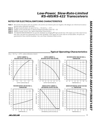
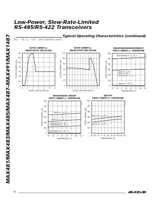
Download to read offline
For free samples & the latest literature: http://www.maxim-ic.com, or phone 1-800-998-8800
_______________General Description
The MAX481, MAX483, MAX485, MAX487–MAX491, and
MAX1487 are low-power transceivers for RS-485 and RS-
422 communication. Each part contains one driver and one
receiver. The MAX483, MAX487, MAX488, and MAX489
feature reduced slew-rate drivers that minimize EMI and
reduce reflections caused by improperly terminated cables,
thus allowing error-free data transmission up to 250kbps.
The driver slew rates of the MAX481, MAX485, MAX490,
MAX491, and MAX1487 are not limited, allowing them to
transmit up to 2.5Mbps.
These transceivers draw between 120µA and 500µA of
supply current when unloaded or fully loaded with disabled
drivers. Additionally, the MAX481, MAX483, and MAX487
have a low-current shutdown mode in which they consume
only 0.1µA. All parts operate from a single 5V supply.
Drivers are short-circuit current limited and are protected
against excessive power dissipation by thermal shutdown
circuitry that places the driver outputs into a high-imped-
ance state. The receiver input has a fail-safe feature that
guarantees a logic-high output if the input is open circuit.
The MAX487 and MAX1487 feature quarter-unit-load
receiver input impedance, allowing up to 128 MAX487/
MAX1487 transceivers on the bus. Full-duplex communi-
cations are obtained using the MAX488–MAX491, while
the MAX481, MAX483, MAX485, MAX487, and MAX1487
are designed for half-duplex applications.
________________________Applications
Low-Power RS-485 Transceivers
Low-Power RS-422 Transceivers
Level Translators
Transceivers for EMI-Sensitive Applications
Industrial-Control Local Area Networks
____________________________Features
o In µMAX Package: Smallest 8-Pin SO
o Slew-Rate Limited for Error-Free Data
Transmission (MAX483/487/488/489)
o 0.1µA Low-Current Shutdown Mode
(MAX481/483/487)
o Low Quiescent Current:
120µA (MAX483/487/488/489)
230µA (MAX1487)
300µA (MAX481/485/490/491)
o -7V to +12V Common-Mode Input Voltage Range
o Three-State Outputs
o 30ns Propagation Delays, 5ns Skew
(MAX481/485/490/491/1487)
o Full-Duplex and Half-Duplex Versions Available
o Operate from a Single 5V Supply
o Allows up to 128 Transceivers on the Bus
(MAX487/MAX1487)
o Current-Limiting and Thermal Shutdown for
Driver Overload Protection
______________Ordering Information
Ordering Information continued at end of data sheet.
* Contact factory for dice specifications.
MAX481/MAX483/MAX485/MAX487–MAX491/MAX1487
Low-Power, Slew-Rate-Limited
RS-485/RS-422 Transceivers
________________________________________________________________ Maxim Integrated Products 1
MAX481
MAX483
MAX485
MAX487
MAX488
MAX489
MAX490
MAX491
MAX1487
PART
NUMBER
HALF/FULL
DUPLEX
DATA RATE
(Mbps)
SLEW-RATE
LIMITED
LOW-POWER
SHUTDOWN
RECEIVER/
DRIVER
ENABLE
QUIESCENT
CURRENT
(µA)
NUMBER OF
TRANSMITTERS
ON BUS
PIN
COUNT
Half
Half
Half
Half
Full
Full
Full
Full
Half
2.5
0.25
2.5
0.25
0.25
0.25
2.5
2.5
2.5
No
Yes
No
Yes
Yes
Yes
No
No
No
Yes
Yes
No
Yes
No
No
No
No
No
Yes
Yes
Yes
Yes
No
Yes
No
Yes
Yes
300
120
300
120
120
120
300
300
230
32
32
32
128
32
32
32
32
128
8
8
8
8
8
14
8
14
8
______________________________________________________________Selection Table
19-0122; Rev 5; 2/96
PART TEMP. RANGE PIN-PACKAGE
MAX481CPA 0°C to +70°C 8 Plastic DIP
MAX481CSA 0°C to +70°C 8 SO
MAX481CUA 0°C to +70°C 8 µMAX
MAX481C/D 0°C to +70°C Dice*
MAX481/MAX483/MAX485/MAX487–MAX491/MAX1487
Low-Power, Slew-Rate-Limited
RS-485/RS-422 Transceivers
2 _______________________________________________________________________________________
ABSOLUTE MAXIMUM RATINGS
Supply Voltage (VCC).............................................................12V
Control Input Voltage (
–
R
—
E
–
, DE)...................-0.5V to (VCC + 0.5V)
Driver Input Voltage (DI).............................-0.5V to (VCC + 0.5V)
Driver Output Voltage (A, B)...................................-8V to +12.5V
Receiver Input Voltage (A, B).................................-8V to +12.5V
Receiver Output Voltage (RO).....................-0.5V to (VCC +0.5V)
Continuous Power Dissipation (TA = +70°C)
8-Pin Plastic DIP (derate 9.09mW/°C above +70°C) ....727mW
14-Pin Plastic DIP (derate 10.00mW/°C above +70°C)..800mW
8-Pin SO (derate 5.88mW/°C above +70°C).................471mW
14-Pin SO (derate 8.33mW/°C above +70°C)...............667mW
8-Pin µMAX (derate 4.1mW/°C above +70°C) ..............830mW
8-Pin CERDIP (derate 8.00mW/°C above +70°C).........640mW
14-Pin CERDIP (derate 9.09mW/°C above +70°C).......727mW
Operating Temperature Ranges
MAX4_ _C_ _/MAX1487C_ A ...............................0°C to +70°C
MAX4_ _E_ _/MAX1487E_ A.............................-40°C to +85°C
MAX4_ _MJ_/MAX1487MJA ...........................-55°C to +125°C
Storage Temperature Range .............................-65°C to +160°C
Lead Temperature (soldering, 10sec) .............................+300°C
DC ELECTRICAL CHARACTERISTICS
(VCC = 5V ±5%, TA = TMIN to TMAX, unless otherwise noted.) (Notes 1, 2)
Stresses beyond those listed under “Absolute Maximum Ratings” may cause permanent damage to the device. These are stress ratings only, and functional
operation of the device at these or any other conditions beyond those indicated in the operational sections of the specifications is not implied. Exposure to
absolute maximum rating conditions for extended periods may affect device reliability.
V
VIN = -7V
VIN = 12V
VIN = -7V
VIN = 12V
Input Current
(A, B)
IIN2
VTH
kΩ48-7V ≤ VCM ≤ 12V, MAX487/MAX1487
RINReceiver Input Resistance
-7V ≤ VCM ≤ 12V, all devices except
MAX487/MAX1487
R = 27Ω (RS-485), Figure 4
0.4V ≤ VO ≤ 2.4V
R = 50Ω (RS-422)
IO = 4mA, VID = -200mV
IO = -4mA, VID = 200mV
VCM = 0V
-7V ≤ VCM ≤ 12V
DE, DI,
–
R
—
E
–
DE, DI,
–
R
—
E
–
MAX487/MAX1487,
DE = 0V, VCC = 0V or 5.25V
DE, DI,
–
R
—
E
–
R = 27Ω or 50Ω, Figure 4
DE = 0V;
VCC = 0V or 5.25V,
all devices except
MAX487/MAX1487
CONDITIONS
kΩ12
µA±1IOZR
Three-State (high impedance)
Output Current at Receiver
V
0.4VOLReceiver Output Low Voltage
3.5VOHReceiver Output High Voltage
mV70∆VTHReceiver Input Hysteresis
V-0.2 0.2
Receiver Differential Threshold
Voltage
-0.2
mA
0.25
mA
-0.8
1.0
1.5 5
VOD2
Differential Driver Output
(with load)
V
2
V5VOD1Differential Driver Output (no load)
µA±2IIN1Input Current
V0.8VILInput Low Voltage
V2.0VIHInput High Voltage
V0.2∆VOD
Change in Magnitude of Driver
Common-Mode Output Voltage
for Complementary Output States
V0.2∆VOD
Change in Magnitude of Driver
Differential Output Voltage for
Complementary Output States
V3VOC
Driver Common-Mode Output
Voltage
UNITSMIN TYP MAXSYMBOLPARAMETER
MAX481/MAX483/MAX485/MAX487–MAX491/MAX1487
Low-Power, Slew-Rate-Limited
RS-485/RS-422 Transceivers
_______________________________________________________________________________________ 3
SWITCHING CHARACTERISTICS—MAX481/MAX485, MAX490/MAX491, MAX1487
(VCC = 5V ±5%, TA = TMIN to TMAX, unless otherwise noted.) (Notes 1, 2)
DC ELECTRICAL CHARACTERISTICS (continued)
(VCC = 5V ±5%, TA = TMIN to TMAX, unless otherwise noted.) (Notes 1, 2)
mA7 950V ≤ VO ≤ VCCIOSRReceiver Short-Circuit Current
mA35 250-7V ≤ VO ≤12V (Note 4)IOSD2
Driver Short-Circuit Current,
VO = Low
mA35 250-7V ≤ VO ≤12V (Note 4)IOSD1
Driver Short-Circuit Current,
VO = High
MAX1487,
–
R
—
E
–
= 0V or VCC
250 400
350 650
ns
10 30 60tPHL
Driver Rise or Fall Time
Figures 6 and 8, RDIFF = 54Ω, CL1 = CL2 = 100pF
ns
MAX490M, MAX491M
MAX490C/E, MAX491C/E 20 90 150
MAX481, MAX485, MAX1487
MAX490M, MAX491M
MAX490C/E, MAX491C/E
MAX481, MAX485, MAX1487
Figures 6 and 8, RDIFF = 54Ω,
CL1 = CL2 = 100pF
MAX481 (Note 5)
Figures 5 and 11, CRL = 15pF, S2 closed
Figures 5 and 11, CRL = 15pF, S1 closed
Figures 5 and 11, CRL = 15pF, S2 closed
Figures 5 and 11, CRL = 15pF, S1 closed
Figures 6 and 10, RDIFF = 54Ω,
CL1 = CL2 = 100pF
Figures 6 and 8,
RDIFF = 54Ω,
CL1 = CL2 = 100pF
Figures 6 and 10,
RDIFF = 54Ω,
CL1 = CL2 = 100pF
CONDITIONS
ns
5 10tSKEW
ns50 200 600tSHDNTime to Shutdown
Mbps2.5fMAXMaximum Data Rate
ns20 50tHZReceiver Disable Time from High
ns
10 30 60tPLH
20 50tLZReceiver Disable Time from Low
ns20 50tZH
Driver Input to Output
Receiver Enable to Output High
ns20 50tZLReceiver Enable to Output Low
20 90 200
ns
ns
13
40 70tHZ
tSKD
Driver Disable Time from High
| tPLH - tPHL | Differential
Receiver Skew
ns40 70tLZDriver Disable Time from Low
ns
40 70tZLDriver Enable to Output Low
3 15 40
ns
5 15 25 ns
3 15 40
tR, tF
20 90 200
Driver Output Skew to Output
tPLH, tPHLReceiver Input to Output
40 70tZHDriver Enable to Output High
UNITSMIN TYP MAXSYMBOLPARAMETER
CONDITIONS UNITSMIN TYP MAXSYMBOLPARAMETER
230 400
300 500
MAX481/MAX485,
–
R
—
E
–
= 0V or VCC
500 900
MAX490/MAX491,
DE, DI,
–
R
—
E
–
= 0V or VCC
300 500
MAX488/MAX489,
DE, DI,
–
R
—
E
–
= 0V or VCC
120 250
DE = VCC
300 500DE = 0V
DE = VCC
DE = 0V
µAMAX481/483/487, DE = 0V,
–
R
—
E
–
= VCC 0.1 10ISHDNSupply Current in Shutdown
120 250
ICC
No-Load Supply Current
(Note 3)
DE = 5V
DE = 0V
MAX483
MAX487
MAX483/MAX487,
–
R
—
E
–
= 0V or VCC
Figures 7 and 9, CL = 100pF, S2 closed
Figures 7 and 9, CL = 100pF, S1 closed
Figures 7 and 9, CL = 15pF, S1 closed
Figures 7 and 9, CL = 15pF, S2 closed
µA
MAX481/MAX483/MAX485/MAX487–MAX491/MAX1487
Low-Power, Slew-Rate-Limited
RS-485/RS-422 Transceivers
4 _______________________________________________________________________________________
SWITCHING CHARACTERISTICS—MAX483, MAX487/MAX488/MAX489
(VCC = 5V ±5%, TA = TMIN to TMAX, unless otherwise noted.) (Notes 1, 2)
SWITCHING CHARACTERISTICS—MAX481/MAX485, MAX490/MAX491, MAX1487 (continued)
(VCC = 5V ±5%, TA = TMIN to TMAX, unless otherwise noted.) (Notes 1, 2)
300 1000
Figures 7 and 9, CL = 100pF, S2 closed
Figures 7 and 9, CL = 100pF, S1 closed
Figures 5 and 11, CL = 15pF, S2 closed,
A - B = 2V
CONDITIONS
ns40 100tZH(SHDN)
Driver Enable from Shutdown to
Output High (MAX481)
ns
Figures 5 and 11, CL = 15pF, S1 closed,
B - A = 2V
tZL(SHDN)
Receiver Enable from Shutdown
to Output Low (MAX481)
ns40 100tZL(SHDN)
Driver Enable from Shutdown to
Output Low (MAX481)
ns300 1000tZH(SHDN)
Receiver Enable from Shutdown
to Output High (MAX481)
UNITSMIN TYP MAXSYMBOLPARAMETER
tPLH
tSKEW
Figures 6 and 8, RDIFF = 54Ω,
CL1 = CL2 = 100pF
tPHL
Figures 6 and 8, RDIFF = 54Ω,
CL1 = CL2 = 100pF
Driver Input to Output
Driver Output Skew to Output ns100 800
ns
ns2000
MAX483/MAX487, Figures 7 and 9,
CL = 100pF, S2 closed
tZH(SHDN)
Driver Enable from Shutdown to
Output High
250 2000
ns2500
MAX483/MAX487, Figures 5 and 11,
CL = 15pF, S1 closed
tZL(SHDN)
Receiver Enable from Shutdown
to Output Low
ns2500
MAX483/MAX487, Figures 5 and 11,
CL = 15pF, S2 closed
tZH(SHDN)
Receiver Enable from Shutdown
to Output High
ns2000
MAX483/MAX487, Figures 7 and 9,
CL = 100pF, S1 closed
tZL(SHDN)
Driver Enable from Shutdown to
Output Low
ns50 200 600MAX483/MAX487 (Note 5)tSHDNTime to Shutdown
tPHL
tPLH, tPHL < 50% of data period
Figures 5 and 11, CRL = 15pF, S2 closed
Figures 5 and 11, CRL = 15pF, S1 closed
Figures 5 and 11, CRL = 15pF, S2 closed
Figures 5 and 11, CRL = 15pF, S1 closed
Figures 7 and 9, CL = 15pF, S2 closed
Figures 6 and 10, RDIFF = 54Ω,
CL1 = CL2 = 100pF
Figures 7 and 9, CL = 15pF, S1 closed
Figures 7 and 9, CL = 100pF, S1 closed
Figures 7 and 9, CL = 100pF, S2 closed
CONDITIONS
kbps250fMAX
250 800 2000
Maximum Data Rate
ns20 50tHZReceiver Disable Time from High
ns
250 800 2000
20 50tLZReceiver Disable Time from Low
ns20 50tZHReceiver Enable to Output High
ns20 50tZLReceiver Enable to Output Low
ns
ns
100
300 3000tHZ
tSKD
Driver Disable Time from High
I tPLH - tPHL I Differential
Receiver Skew
Figures 6 and 10, RDIFF = 54Ω,
CL1 = CL2 = 100pF
ns300 3000tLZDriver Disable Time from Low
ns250 2000tZLDriver Enable to Output Low
ns
Figures 6 and 8, RDIFF = 54Ω,
CL1 = CL2 = 100pF
ns250 2000tR, tF
250 2000
Driver Rise or Fall Time
ns
tPLH
Receiver Input to Output
250 2000tZHDriver Enable to Output High
UNITSMIN TYP MAXSYMBOLPARAMETER
MAX481/MAX483/MAX485/MAX487–MAX491/MAX1487
Low-Power, Slew-Rate-Limited
RS-485/RS-422 Transceivers
_______________________________________________________________________________________ 5
30
0
0 2.5
OUTPUT CURRENT vs.
RECEIVER OUTPUT LOW VOLTAGE
5
25
MAX481-01
OUTPUT LOW VOLTAGE (V)
OUTPUTCURRENT(mA)
1.5
15
10
0.5 1.0 2.0
20
35
40
45
0.9
0.1
-50 -25 25 75
RECEIVER OUTPUT LOW VOLTAGE vs.
TEMPERATURE
0.3
0.7
TEMPERATURE (°C)
OUTPUTLOWVOLTAGE(V)
0 50
0.5
0.8
0.2
0.6
0.4
0
100 125
MAX481-04
IRO = 8mA
-20
-4
1.5 2.0 3.0 5.0
OUTPUT CURRENT vs.
RECEIVER OUTPUT HIGH VOLTAGE
-8
-16
MAX481-02
OUTPUT HIGH VOLTAGE (V)
OUTPUTCURRENT(mA)
2.5 4.0
-12
-18
-6
-14
-10
-2
0
3.5 4.5
4.8
3.2
-50 -25 25 75
RECEIVER OUTPUT HIGH VOLTAGE vs.
TEMPERATURE
3.6
4.4
TEMPERATURE (°C)
OUTPUTHIGHVOLTAGE(V)
0 50
4.0
4.6
3.4
4.2
3.8
3.0
100 125
MAX481-03
IRO = 8mA
90
0
0 1.0 3.0 4.5
DRIVER OUTPUT CURRENT vs.
DIFFERENTIAL OUTPUT VOLTAGE
10
70
MAX481-05
DIFFERENTIAL OUTPUT VOLTAGE (V)
OUTPUTCURRENT(mA)
2.0 4.0
50
30
80
60
40
20
0.5 1.5 2.5 3.5
2.3
1.5
-50 -25 25 125
DRIVER DIFFERENTIAL OUTPUT VOLTAGE
vs. TEMPERATURE
1.7
2.1
MAX481-06
TEMPERATURE (°C)
DIFFERENTIALOUTPUTVOLTAGE(V)
0 75
1.9
2.2
1.6
2.0
1.8
10050
2.4
R = 54Ω
__________________________________________Typical Operating Characteristics
(VCC = 5V, TA = +25°C, unless otherwise noted.)
NOTES FOR ELECTRICAL/SWITCHING CHARACTERISTICS
Note 1: All currents into device pins are positive; all currents out of device pins are negative. All voltages are referenced to device
ground unless otherwise specified.
Note 2: All typical specifications are given for VCC = 5V and TA = +25°C.
Note 3: Supply current specification is valid for loaded transmitters when DE = 0V.
Note 4: Applies to peak current. See Typical Operating Characteristics.
Note 5: The MAX481/MAX483/MAX487 are put into shutdown by bringing
–
R
—
E
–
high and DE low. If the inputs are in this state for less
than 50ns, the parts are guaranteed not to enter shutdown. If the inputs are in this state for at least 600ns, the parts are
guaranteed to have entered shutdown. See Low-Power Shutdown Mode section.
MAX481/MAX483/MAX485/MAX487–MAX491/MAX1487
Low-Power, Slew-Rate-Limited
RS-485/RS-422 Transceivers
6 _______________________________________________________________________________________
____________________________Typical Operating Characteristics (continued)
(VCC = 5V, TA = +25°C, unless otherwise noted.)
120
0
0 8
OUTPUT CURRENT vs.
DRIVER OUTPUT LOW VOLTAGE
20
100
MAX481-07
OUTPUT LOW VOLTAGE (V)
OUTPUTCURRENT(mA)
6
60
40
2 4
80
10 12
140 -120
0
-7 -5 -1 5
OUTPUT CURRENT vs.
DRIVER OUTPUT HIGH VOLTAGE
-20
-80
MAX481-08
OUTPUT HIGH VOLTAGE (V)
OUTPUTCURRENT(mA)
-3 1
-60
3-6 -4 -2 0 2 4
-100
-40
100
-40-60 -20 40 100 120
MAX1487
SUPPLY CURRENT vs. TEMPERATURE
300
MAX481-13
TEMPERATURE (°C)
SUPPLYCURRENT(µA)
20 60 80
500
200
600
400
0
0 140
MAX1487; DE = VCC, RE = X
MAX1487; DE = 0V, RE = X
100
-50 -25 50 100
MAX481/MAX485/MAX490/MAX491
SUPPLY CURRENT vs. TEMPERATURE
300
MAX481-11
TEMPERATURE (°C)
SUPPLYCURRENT(µA)
25 75
500
200
600
400
0
0 125
MAX481/MAX485; DE = VCC, RE = X
MAX485; DE = 0, RE = X,
MAX481; DE = RE = 0
MAX490/MAX491; DE = RE = X
MAX481; DE = 0, RE = VCC
100
-50 -25 50 100
MAX483/MAX487–MAX489
SUPPLY CURRENT vs. TEMPERATURE
300
MAX481-12
TEMPERATURE (°C)
SUPPLYCURRENT(µA)
25 75
500
200
600
400
0
0 125
MAX483; DE = VCC, RE = X
MAX487; DE = VCC, RE = X
MAX483/MAX487; DE = 0, RE = VCC
MAX483/MAX487; DE = RE = 0,
MAX488/MAX489; DE = RE = X
MAX481/MAX483/MAX485/MAX487–MAX491/MAX1487
Low-Power, Slew-Rate-Limited
RS-485/RS-422 Transceivers
_______________________________________________________________________________________ 7
______________________________________________________________Pin Description
MAX481
MAX483
MAX485
MAX487
MAX1487
TOP VIEW
NOTE: PIN LABELS Y AND Z ON TIMING, TEST, AND WAVEFORM DIAGRAMS REFER TO PINS A AND B WHEN DE IS HIGH.
TYPICAL OPERATING CIRCUIT SHOWN WITH DIP/SO PACKAGE.
1
2
3
4
8
5
VCC
GNDDI
DE
RE
RO R
D
RtRt
7
6
D
R
DE
RE
DI
ROA
B
1
2
3
4
8
7
6
5
VCC
B
A
GNDDI
DE
RE
RO
DIP/SO
R
D
1
2
3
4
8
7
6
5
VCC
A
GND
DERE
B
RO
µMAX
B
A
DI
MAX481
MAX483
MAX485
MAX487
MAX1487
Figure 1. MAX481/MAX483/MAX485/MAX487/MAX1487 Pin Configuration and Typical Operating Circuit
µMAX
—
—
5
6
7
8
—
2
—
1
3
—
µMAX
4
5
6
7
—
—
8
—
1
—
2
—
DIP/SO DIP/SO
2 3
Receiver Output Enable. RO is enabled when
–
R
—
E
–
is low; RO is
high impedance when
–
R
—
E
–
is high.
3 4
Driver Output Enable. The driver outputs, Y and Z, are enabled
by bringing DE high. They are high impedance when DE is low. If
the driver outputs are enabled, the parts function as line drivers.
While they are high impedance, they function as line receivers if
–
R
—
E
–
is low.
DIP/SO
—
4 5
Driver Input. A low on DI forces output Y low and output Z high.
Similarly, a high on DI forces output Y high and output Z low.
5 6, 7 Ground
— 9 Noninverting Driver Output
— 10 Inverting Driver Output
—
3
4
6 — Noninverting Receiver Input and Noninverting Driver Output
— 12 Noninverting Receiver Input
5
6
—
8
–
R
—
E
–
DE
DI
GND
Y
Z
A
A
7 — — B Inverting Receiver Input and Inverting Driver Output
— 7 11 B Inverting Receiver Input
8 1 14 VCC Positive Supply: 4.75V ≤ VCC ≤ 5.25V
— — 1, 8, 13 N.C. No Connect—not internally connected
FUNCTIONNAME
431 2
Receiver Output: If A > B by 200mV, RO will be high;
If A < B by 200mV, RO will be low.
2 RO
PIN
FUNCTIONNAME
MAX481/MAX483/
MAX485/MAX487/
MAX1487
MAX488/
MAX490
MAX489/
MAX491
MAX481/MAX483/MAX485/MAX487–MAX491/MAX1487
__________Applications Information
The MAX481/MAX483/MAX485/MAX487–MAX491 and
MAX1487 are low-power transceivers for RS-485 and RS-
422 communications. The MAX481, MAX485, MAX490,
MAX491, and MAX1487 can transmit and receive at data
rates up to 2.5Mbps, while the MAX483, MAX487,
MAX488, and MAX489 are specified for data rates up to
250kbps. The MAX488–MAX491 are full-duplex trans-
ceivers while the MAX481, MAX483, MAX485, MAX487,
and MAX1487 are half-duplex. In addition, Driver Enable
(DE) and Receiver Enable (RE) pins are included on the
MAX481, MAX483, MAX485, MAX487, MAX489,
MAX491, and MAX1487. When disabled, the driver and
receiver outputs are high impedance.
MAX487/MAX1487:
128 Transceivers on the Bus
The 48kΩ, 1/4-unit-load receiver input impedance of the
MAX487 and MAX1487 allows up to 128 transceivers
on a bus, compared to the 1-unit load (12kΩ input
impedance) of standard RS-485 drivers (32 trans-
ceivers maximum). Any combination of MAX487/
MAX1487 and other RS-485 transceivers with a total of
32 unit loads or less can be put on the bus. The
MAX481/MAX483/MAX485 and MAX488–MAX491 have
standard 12kΩ Receiver Input impedance.
Low-Power, Slew-Rate-Limited
RS-485/RS-422 Transceivers
8 _______________________________________________________________________________________
MAX488
MAX490
TOP VIEW
1
2
3
4
RO
DI
GND
8
7
6
5
A
B
Z
Y
VCC
DIP/SO
R
D
Rt
Rt
VCC
5
6
7
8
RO
DI
GND
4
GND
DI
RO
3
2
A
B
Y
Z
VCC
D R
R D
1
3VCC
4RO
2A
1
6
5
7
8
GND
DI
Y
ZB
µMAX
MAX488
MAX490
NOTE: TYPICAL OPERATING CIRCUIT SHOWN WITH DIP/SO PACKAGE.
MAX489
MAX491
DIP/SO
TOP VIEW
Rt
Rt
DE VCC
RE GND
VCC RE
GND DE
RO
DI
9
10
12
11
B
A
Z
Y
5
RO
NC
DI
2
1, 8, 13
3 6, 7
144
1
2
3
4
5
6
7
14
13
12
11
10
9
8
VCC
N.C.
N.C.
A
B
Z
Y
N.C.
RO
RE
DE
DI
GND
GND
R
D
D
R D
R
Figure 2. MAX488/MAX490 Pin Configuration and Typical Operating Circuit
Figure 3. MAX489/MAX491 Pin Configuration and Typical Operating Circuit
MAX483/MAX487/MAX488/MAX489:
Reduced EMI and Reflections
The MAX483 and MAX487–MAX489 are slew-rate limit-
ed, minimizing EMI and reducing reflections caused by
improperly terminated cables. Figure 12 shows the dri-
ver output waveform and its Fourier analysis of a
150kHz signal transmitted by a MAX481, MAX485,
MAX490, MAX491, or MAX1487. High-frequency har-
monics with large amplitudes are evident. Figure 13
shows the same information displayed for a MAX483,
MAX487, MAX488, or MAX489 transmitting under the
same conditions. Figure 13’s high-frequency harmonics
have much lower amplitudes, and the potential for EMI
is significantly reduced.
MAX481/MAX483/MAX485/MAX487–MAX491/MAX1487
Low-Power, Slew-Rate-Limited
RS-485/RS-422 Transceivers
_______________________________________________________________________________________ 9
R
R
Y
Z
VOD
VOC
RECEIVER
OUTPUT
TEST POINT
1k
1k
S1
S2
VCC
CRL
15pF
DI
DE
3V
Y
Z
CL1
CL2
A
B
RO
RE
RDIFF
VID
OUTPUT
UNDER TEST
500Ω S1
S2
VCC
CL
_________________________________________________________________Test Circuits
Figure 4. Driver DC Test Load Figure 5. Receiver Timing Test Load
Figure 6. Driver/Receiver Timing Test Circuit Figure 7. Driver Timing Test Load
MAX481/MAX483/MAX485/MAX487–MAX491/MAX1487
Low-Power, Slew-Rate-Limited
RS-485/RS-422 Transceivers
10 ______________________________________________________________________________________
_______________________________________________________Switching Waveforms
DI
3V
0V
Z
Y
VO
0V
-VO
VO
1.5V
tPLH
1/2 VO
10%
tR
90% 90%
tPHL
1.5V
1/2 VO
10%
tF
VDIFF = V (Y) - V (Z)
VDIFF
tSKEW = | tPLH - tPHL |
OUTPUT NORMALLY LOW
OUTPUT NORMALLY HIGH
3V
0V
Y, Z
VOL
Y, Z
0V
1.5V 1.5V
VOL +0.5V
VOH -0.5V2.3V
2.3V
tZL(SHDN), tZL tLZ
tZH(SHDN), tZH tHZ
DE
VOH
VOL
VID
-VID
1.5V
0V
1.5VOUTPUT
INPUT 0V
RO
A-B
tPLHtPHL
OUTPUT NORMALLY LOW
OUTPUT NORMALLY HIGH
3V
0V
VCC
RO
RO
0V
1.5V 1.5V
VOL + 0.5V
VOH - 0.5V1.5V
1.5V
tZL(SHDN), tZL tLZ
tZH(SHDN), tZH tHZ
RE
_________________Function Tables (MAX481/MAX483/MAX485/MAX487/MAX1487)
Figure 8. Driver Propagation Delays Figure 9. Driver Enable and Disable Times (except MAX488 and
MAX490)
Figure 10. Receiver Propagation Delays Figure 11. Receiver Enable and Disable Times (except MAX488
and MAX490)
Table 1. Transmitting Table 2. Receiving
INPUTS OUTPUT
RE DE A-B RO
0
0
0
1
0
0
0
0
> +0.2V
< -0.2V
Inputs open
X
1
0
1
High-Z*
X = Don't care
High-Z = High impedance
* Shutdown mode for MAX481/MAX483/MAX487
INPUTS OUTPUTS
RE DE DI Z Y
X
X
0
1
1
1
0
0
1
0
X
X
0
1
High-Z
High-Z*
1
0
High-Z
High-Z*
X = Don't care
High-Z = High impedance
* Shutdown mode for MAX481/MAX483/MAX487
Low-Power Shutdown Mode
(MAX481/MAX483/MAX487)
A low-power shutdown mode is initiated by bringing
both
–
R
—
E
–
high and DE low. The devices will not shut
down unless both the driver and receiver are disabled.
In shutdown, the devices typically draw only 0.1µA of
supply current.
–
R
—
E
–
and DE may be driven simultaneously; the parts are
guaranteed not to enter shutdown if
–
R
—
E
–
is high and DE
is low for less than 50ns. If the inputs are in this state
for at least 600ns, the parts are guaranteed to enter
shutdown.
For the MAX481, MAX483, and MAX487, the tZH and
tZL enable times assume the part was not in the low-
power shutdown state (the MAX485/MAX488–MAX491
and MAX1487 can not be shut down). The tZH(SHDN)
and tZL(SHDN) enable times assume the parts were shut
down (see Electrical Characteristics).
It takes the drivers and receivers longer to become
enabled from the low-power shutdown state
(tZH(SHDN), tZL(SHDN)) than from the operating mode
(tZH, tZL). (The parts are in operating mode if the
–
R
—
E
–
,
DE inputs equal a logical 0,1 or 1,1 or 0, 0.)
Driver Output Protection
Excessive output current and power dissipation caused
by faults or by bus contention are prevented by two
mechanisms. A foldback current limit on the output
stage provides immediate protection against short cir-
cuits over the whole common-mode voltage range (see
Typical Operating Characteristics). In addition, a ther-
mal shutdown circuit forces the driver outputs into a
high-impedance state if the die temperature rises
excessively.
Propagation Delay
Many digital encoding schemes depend on the differ-
ence between the driver and receiver propagation
delay times. Typical propagation delays are shown in
Figures 15–18 using Figure 14’s test circuit.
The difference in receiver delay times, | tPLH - tPHL |, is
typically under 13ns for the MAX481, MAX485,
MAX490, MAX491, and MAX1487 and is typically less
than 100ns for the MAX483 and MAX487–MAX489.
The driver skew times are typically 5ns (10ns max) for
the MAX481, MAX485, MAX490, MAX491, and
MAX1487, and are typically 100ns (800ns max) for the
MAX483 and MAX487–MAX489.
MAX481/MAX483/MAX485/MAX487–MAX491/MAX1487
Low-Power, Slew-Rate-Limited
RS-485/RS-422 Transceivers
______________________________________________________________________________________ 11
10dB/div
0Hz 5MHz
500kHz/div
10dB/div
0Hz 5MHz
500kHz/div
Figure 12. Driver Output Waveform and FFT Plot of MAX481/
MAX485/MAX490/MAX491/MAX1487 Transmitting a 150kHz
Signal
Figure 13. Driver Output Waveform and FFT Plot of MAX483/
MAX487–MAX489 Transmitting a 150kHz Signal
MAX481/MAX483/MAX485/MAX487–MAX491/MAX1487
Low-Power, Slew-Rate-Limited
RS-485/RS-422 Transceivers
12 ______________________________________________________________________________________
TTL IN
tR, tF < 6ns D R
100pF
B
100pF
A
RECEIVER
OUT
R = 54Ω
Z
Y
500mV/div
20ns/div
A
B
RO
2V/div
VCC = 5V
TA = +25°C 500mV/div
20ns/div
A
B
RO
2V/div
VCC = 5V
TA = +25°C
500mV/div
400ns/div
A
B
RO
2V/div
VCC = 5V
TA = +25°C
500mV/div
400ns/div
A
B
RO
2V/div
VCC = 5V
TA = +25°C
Figure 14. Receiver Propagation Delay Test Circuit
Figure 15. MAX481/MAX485/MAX490/MAX491/MAX1487
Receiver tPHL
Figure 16. MAX481/MAX485/MAX490/MAX491/MAX1487
Receiver tPLH
Figure 17. MAX483, MAX487–MAX489 Receiver tPHL Figure 18. MAX483, MAX487–MAX489 Receiver tPLH
Line Length vs. Data Rate
The RS-485/RS-422 standard covers line lengths up to
4000 feet. For line lengths greater than 4000 feet, see
Figure 23.
Figures 19 and 20 show the system differential voltage
for the parts driving 4000 feet of 26AWG twisted-pair
wire at 110kHz into 120Ω loads.
Typical Applications
The MAX481, MAX483, MAX485, MAX487–MAX491, and
MAX1487 transceivers are designed for bidirectional data
communications on multipoint bus transmission lines.
Figures 21 and 22 show typical network applications
circuits. These parts can also be used as line
repeaters, with cable lengths longer than 4000 feet, as
shown in Figure 23.
To minimize reflections, the line should be terminated at
both ends in its characteristic impedance, and stub
lengths off the main line should be kept as short as possi-
ble. The slew-rate-limited MAX483 and MAX487–MAX489
are more tolerant of imperfect termination.
MAX481/MAX483/MAX485/MAX487–MAX491/MAX1487
Low-Power, Slew-Rate-Limited
RS-485/RS-422 Transceivers
______________________________________________________________________________________ 13
DI
VY-VZ
RO
5V
0V
1V
0V
-1V
5V
0V
2µs/div
DI
VY-VZ
RO
5V
0V
1V
0V
-1V
5V
0V
2µs/div
DI RO DE
RE
A
B
RE
RERE
RO
RO
RO
DI
DI
DI
DE
DE
DE
D D
D
RR
R
B B
B
AAA
120Ω 120Ω
D
R
MAX481
MAX483
MAX485
MAX487
MAX1487
Figure 19. MAX481/MAX485/MAX490/MAX491/MAX1487
System Differential Voltage at 110kHz Driving 4000ft of Cable
Figure 20. MAX483, MAX487–MAX489 System Differential
Voltage at 110kHz Driving 4000ft of Cable
Figure 21. MAX481/MAX483/MAX485/MAX487/MAX1487 Typical Half-Duplex RS-485 Network
MAX481/MAX483/MAX485/MAX487–MAX491/MAX1487
Low-Power, Slew-Rate-Limited
RS-485/RS-422 Transceivers
14 ______________________________________________________________________________________
Figure 22. MAX488–MAX491 Full-Duplex RS-485 Network
120Ω 120Ω
R
D
RO
RE
DE
DI
A
B
Y
120Ω 120ΩDI
DI DIRO RO
RO
DE DE
DE
RE
RE
RE
Z
Z
Z
Z
Y
Y
Y
A A
A
B B
B
D D
D
R R
R
MAX488
MAX489
MAX490
MAX491
NOTE: RE AND DE ON MAX489/MAX491 ONLY.
Figure 23. Line Repeater for MAX488–MAX491
120Ω
120Ω
DATA IN
DATA OUT
R
D
RO
RE
DE
DI
A
B
Z
Y
MAX488–MAX491
NOTE: RE AND DE ON MAX489/MAX491 ONLY.
Isolated RS-485
For isolated RS-485 applications, see the MAX253 and
MAX1480 data sheets.
MAX481/MAX483/MAX485/MAX487–MAX491/MAX1487
Low-Power, Slew-Rate-Limited
RS-485/RS-422 Transceivers
______________________________________________________________________________________ 15
__Ordering Information (continued)
_________________Chip Topographies
MAX481/MAX483/MAX485/MAX487/MAX1487
N.C.
RO
0.054"
(1.372mm)
0.080"
(2.032mm)
DE
DI
GND
B
N.C.
VCC
A
RE
* Contact factory for dice specifications.
14 CERDIP-55°C to +125°CMAX489MJD
14 SO-40°C to +85°CMAX489ESD
14 Plastic DIP-40°C to +85°CMAX489EPD
Dice*0°C to +70°CMAX489C/D
14 SO0°C to +70°CMAX489CSD
14 Plastic DIP0°C to +70°CMAX489CPD
8 CERDIP-55°C to +125°CMAX488MJA
8 SO-40°C to +85°CMAX488ESA
8 Plastic DIP-40°C to +85°CMAX488EPA
Dice*0°C to +70°CMAX488C/D
8 SO0°C to +70°CMAX488CSA
8 Plastic DIP0°C to +70°CMAX488CPA
8 CERDIP-55°C to +125°CMAX487MJA
8 SO-40°C to +85°CMAX487ESA
8 Plastic DIP-40°C to +85°CMAX487EPA
Dice*0°C to +70°CMAX487C/D
8 SO0°C to +70°CMAX487CSA
8 Plastic DIP0°C to +70°CMAX487CPA
8 CERDIP-55°C to +125°CMAX485MJA
8 SO-40°C to +85°CMAX485ESA
8 Plastic DIP-40°C to +85°CMAX485EPA
Dice*0°C to +70°CMAX485C/D
8 SO0°C to +70°CMAX485CSA
8 Plastic DIP0°C to +70°CMAX485CPA
8 CERDIP-55°C to +125°CMAX483MJA
8 SO-40°C to +85°CMAX483ESA
8 Plastic DIP-40°C to +85°CMAX483EPA
8 CERDIP-55°C to +125°CMAX481MJA
8 Plastic DIP-40°C to +85°CMAX481EPA
PIN-PACKAGETEMP. RANGEPART
14 CERDIP-55°C to +125°CMAX491MJD
14 SO-40°C to +85°CMAX491ESD
14 Plastic DIP-40°C to +85°CMAX491EPD
Dice*0°C to +70°CMAX491C/D
14 SO0°C to +70°CMAX491CSD
14 Plastic DIP0°C to +70°CMAX491CPD
8 CERDIP-55°C to +125°CMAX490MJA
8 SO-40°C to +85°CMAX490ESA
8 Plastic DIP-40°C to +85°CMAX490EPA
Dice*0°C to +70°CMAX490C/D
8 Plastic DIP0°C to +70°CMAX490CPA
PIN-PACKAGETEMP. RANGEPART
8 SO-40°C to +85°CMAX481ESA
8 µMAX0°C to +70°CMAX485CUA
8 µMAX0°C to +70°CMAX487CUA
8 µMAX0°C to +70°CMAX488CUA
8 SO0°C to +70°CMAX490CSA
8 µMAX0°C to +70°CMAX490CUA
__Ordering Information (continued)
8 CERDIP-55°C to +125°CMAX1487MJA
8 SO-40°C to +85°CMAX1487ESA
8 Plastic DIP-40°C to +85°CMAX1487EPA
Dice*0°C to +70°CMAX1487C/D
8 SO0°C to +70°CMAX1487CSA
8 Plastic DIP0°C to +70°CMAX1487CPA
8 µMAX0°C to +70°CMAX1487CUA
8 µMAX0°C to +70°CMAX483CUA
Dice*0°C to +70°CMAX483C/D
8 SO0°C to +70°CMAX483CSA
8 Plastic DIP0°C to +70°CMAX483CPA
Maxim cannot assume responsibility for use of any circuitry other than circuitry entirely embodied in a Maxim product. No circuit patent licenses are
implied. Maxim reserves the right to change the circuitry and specifications without notice at any time.
16 __________________Maxim Integrated Products, 120 San Gabriel Drive, Sunnyvale, CA 94086 (408) 737-7600
© 1996 Maxim Integrated Products Printed USA is a registered trademark of Maxim Integrated Products.
MAX481/MAX483/MAX485/MAX487–MAX491/MAX1487
Low-Power, Slew-Rate-Limited
RS-485/RS-422 Transceivers
________________________________________________________Package Information
L
α
C
A1B
DIM
A
A1
B
C
D
E
e
H
L
α
MIN
0.036
0.004
0.010
0.005
0.116
0.116
0.188
0.016
0°
MAX
0.044
0.008
0.014
0.007
0.120
0.120
0.198
0.026
6°
MIN
0.91
0.10
0.25
0.13
2.95
2.95
4.78
0.41
0°
MAX
1.11
0.20
0.36
0.18
3.05
3.05
5.03
0.66
6°
INCHES MILLIMETERS
8-PIN µMAX
MICROMAX SMALL-OUTLINE
PACKAGE
0.650.0256
A
e
E H
D
0.101mm
0.004 in
21-0036D
TRANSISTOR COUNT: 248
SUBSTRATE CONNECTED TO GND
MAX488/MAX490
B
RO
0.054"
(1.372mm)
0.080"
(2.032mm)
N.C.
DI
GND
Z
A
VCC
Y
N.C.
_____________________________________________Chip Topographies (continued)
MAX489/MAX491
B
RO
0.054"
(1.372mm)
0.080"
(2.032mm)
DE
DI
GND
Z
A
VCC
Y
RE

More Related Content

What's hot

Intelligent mcc Siemens
Intelligent mcc Siemens Intelligent mcc Siemens
Intelligent mcc Siemens Praveen Patil
 
Overview Study on Single-Channel I2C to 1-Wire Master DS2482
Overview Study on Single-Channel I2C to 1-Wire Master DS2482Overview Study on Single-Channel I2C to 1-Wire Master DS2482
Overview Study on Single-Channel I2C to 1-Wire Master DS2482Premier Farnell
 
KYL-200L wireless data transmission RF module for 2-3km
KYL-200L wireless data transmission RF module for 2-3km KYL-200L wireless data transmission RF module for 2-3km
KYL-200L wireless data transmission RF module for 2-3km Minerva Zhao
 
Shenzhen Hifibercom Technology Co.,Ltd Qsfp28 CWDM4 optical module
Shenzhen Hifibercom Technology Co.,Ltd  Qsfp28 CWDM4 optical moduleShenzhen Hifibercom Technology Co.,Ltd  Qsfp28 CWDM4 optical module
Shenzhen Hifibercom Technology Co.,Ltd Qsfp28 CWDM4 optical moduleWendyXia8
 
LayerZero Series 70 ePODs: Type-P Power Distribution Unit with Transformer an...
LayerZero Series 70 ePODs: Type-P Power Distribution Unit with Transformer an...LayerZero Series 70 ePODs: Type-P Power Distribution Unit with Transformer an...
LayerZero Series 70 ePODs: Type-P Power Distribution Unit with Transformer an...LayerZero Power Systems, Inc.
 
Zxr10 introduction to 5928 e
Zxr10 introduction to 5928 eZxr10 introduction to 5928 e
Zxr10 introduction to 5928 eMeshack Omingo
 
Microcontroller Based Devices By Novatek Electro (India) Pvt. Ltd, Delhi
Microcontroller Based Devices By Novatek Electro (India) Pvt. Ltd, DelhiMicrocontroller Based Devices By Novatek Electro (India) Pvt. Ltd, Delhi
Microcontroller Based Devices By Novatek Electro (India) Pvt. Ltd, DelhiIndiaMART InterMESH Limited
 
INTELLIGENT POWER MODULE Model No : PEC16DSMO1
INTELLIGENT POWER MODULE Model No : PEC16DSMO1 INTELLIGENT POWER MODULE Model No : PEC16DSMO1
INTELLIGENT POWER MODULE Model No : PEC16DSMO1 MayankSunhare
 
Weg electronic-relays-50058082-brochure-english
Weg electronic-relays-50058082-brochure-englishWeg electronic-relays-50058082-brochure-english
Weg electronic-relays-50058082-brochure-englishAllan Bernardino
 
QuickSilver Controls QCI-DS030 QCI-X23
QuickSilver Controls QCI-DS030 QCI-X23 QuickSilver Controls QCI-DS030 QCI-X23
QuickSilver Controls QCI-DS030 QCI-X23 Electromate
 
AODesign&Protection_2015_noNDA
AODesign&Protection_2015_noNDAAODesign&Protection_2015_noNDA
AODesign&Protection_2015_noNDAKevin Duke
 

What's hot (20)

Intelligent mcc Siemens
Intelligent mcc Siemens Intelligent mcc Siemens
Intelligent mcc Siemens
 
ABB Relay
ABB RelayABB Relay
ABB Relay
 
Overview Study on Single-Channel I2C to 1-Wire Master DS2482
Overview Study on Single-Channel I2C to 1-Wire Master DS2482Overview Study on Single-Channel I2C to 1-Wire Master DS2482
Overview Study on Single-Channel I2C to 1-Wire Master DS2482
 
05 nrms install
05 nrms install05 nrms install
05 nrms install
 
Bts fault codes
Bts fault codesBts fault codes
Bts fault codes
 
KYL-200L wireless data transmission RF module for 2-3km
KYL-200L wireless data transmission RF module for 2-3km KYL-200L wireless data transmission RF module for 2-3km
KYL-200L wireless data transmission RF module for 2-3km
 
Shenzhen Hifibercom Technology Co.,Ltd Qsfp28 CWDM4 optical module
Shenzhen Hifibercom Technology Co.,Ltd  Qsfp28 CWDM4 optical moduleShenzhen Hifibercom Technology Co.,Ltd  Qsfp28 CWDM4 optical module
Shenzhen Hifibercom Technology Co.,Ltd Qsfp28 CWDM4 optical module
 
LayerZero Series 70 ePODs: Type-P Power Distribution Unit with Transformer an...
LayerZero Series 70 ePODs: Type-P Power Distribution Unit with Transformer an...LayerZero Series 70 ePODs: Type-P Power Distribution Unit with Transformer an...
LayerZero Series 70 ePODs: Type-P Power Distribution Unit with Transformer an...
 
Scada
ScadaScada
Scada
 
Zxr10 introduction to 5928 e
Zxr10 introduction to 5928 eZxr10 introduction to 5928 e
Zxr10 introduction to 5928 e
 
Microcontroller Based Devices By Novatek Electro (India) Pvt. Ltd, Delhi
Microcontroller Based Devices By Novatek Electro (India) Pvt. Ltd, DelhiMicrocontroller Based Devices By Novatek Electro (India) Pvt. Ltd, Delhi
Microcontroller Based Devices By Novatek Electro (India) Pvt. Ltd, Delhi
 
INTELLIGENT POWER MODULE Model No : PEC16DSMO1
INTELLIGENT POWER MODULE Model No : PEC16DSMO1 INTELLIGENT POWER MODULE Model No : PEC16DSMO1
INTELLIGENT POWER MODULE Model No : PEC16DSMO1
 
Weg electronic-relays-50058082-brochure-english
Weg electronic-relays-50058082-brochure-englishWeg electronic-relays-50058082-brochure-english
Weg electronic-relays-50058082-brochure-english
 
Datasheet bq33200
Datasheet bq33200Datasheet bq33200
Datasheet bq33200
 
320 lecture7
320 lecture7320 lecture7
320 lecture7
 
QuickSilver Controls QCI-DS030 QCI-X23
QuickSilver Controls QCI-DS030 QCI-X23 QuickSilver Controls QCI-DS030 QCI-X23
QuickSilver Controls QCI-DS030 QCI-X23
 
NFS2-3030
NFS2-3030NFS2-3030
NFS2-3030
 
DVC
DVCDVC
DVC
 
AODesign&Protection_2015_noNDA
AODesign&Protection_2015_noNDAAODesign&Protection_2015_noNDA
AODesign&Protection_2015_noNDA
 
NFS-320
NFS-320NFS-320
NFS-320
 

Similar to Max485ds

Similar to Max485ds (20)

A4988
A4988A4988
A4988
 
ABB PVI
ABB PVIABB PVI
ABB PVI
 
AN-9754
AN-9754AN-9754
AN-9754
 
PVI-10
PVI-10PVI-10
PVI-10
 
Max232
Max232Max232
Max232
 
Advanced motion controls_azbh10a4
Advanced motion controls_azbh10a4Advanced motion controls_azbh10a4
Advanced motion controls_azbh10a4
 
Trio 20.0-27
Trio 20.0-27Trio 20.0-27
Trio 20.0-27
 
Trio 20.0-tl-outd-400
Trio 20.0-tl-outd-400Trio 20.0-tl-outd-400
Trio 20.0-tl-outd-400
 
Ad598
Ad598Ad598
Ad598
 
Ucc 3895 dw
Ucc 3895 dwUcc 3895 dw
Ucc 3895 dw
 
As15 f
As15 fAs15 f
As15 f
 
sfp-2.5g-sx-850nm-550m-optical-transceiver-151009.pdf
sfp-2.5g-sx-850nm-550m-optical-transceiver-151009.pdfsfp-2.5g-sx-850nm-550m-optical-transceiver-151009.pdf
sfp-2.5g-sx-850nm-550m-optical-transceiver-151009.pdf
 
sfp-1g-zx-1550nm-80km-optical-transceiver-151004.pdf
sfp-1g-zx-1550nm-80km-optical-transceiver-151004.pdfsfp-1g-zx-1550nm-80km-optical-transceiver-151004.pdf
sfp-1g-zx-1550nm-80km-optical-transceiver-151004.pdf
 
Advanced motion controls 5a5
Advanced motion controls 5a5Advanced motion controls 5a5
Advanced motion controls 5a5
 
Abb trio-tl-outd
Abb trio-tl-outdAbb trio-tl-outd
Abb trio-tl-outd
 
Advanced motion controls az60a8
Advanced motion controls az60a8Advanced motion controls az60a8
Advanced motion controls az60a8
 
Advanced motion controls 10a8
Advanced motion controls 10a8Advanced motion controls 10a8
Advanced motion controls 10a8
 
sfp-1g-cwdm-1430nm-80km-optical-transceiver-151049.pdf
sfp-1g-cwdm-1430nm-80km-optical-transceiver-151049.pdfsfp-1g-cwdm-1430nm-80km-optical-transceiver-151049.pdf
sfp-1g-cwdm-1430nm-80km-optical-transceiver-151049.pdf
 
sfp-1g-cwdm-1490nm-80km-fiber-optic-transceiver-151052.pdf
sfp-1g-cwdm-1490nm-80km-fiber-optic-transceiver-151052.pdfsfp-1g-cwdm-1490nm-80km-fiber-optic-transceiver-151052.pdf
sfp-1g-cwdm-1490nm-80km-fiber-optic-transceiver-151052.pdf
 
Electrocraft pro a08_v48_datasheet
Electrocraft pro a08_v48_datasheetElectrocraft pro a08_v48_datasheet
Electrocraft pro a08_v48_datasheet
 

More from ____

2019 c1 info_prova_escrita
2019 c1 info_prova_escrita2019 c1 info_prova_escrita
2019 c1 info_prova_escrita____
 
Documento1
Documento1Documento1
Documento1____
 
Boe a-2018-13593-c
Boe a-2018-13593-cBoe a-2018-13593-c
Boe a-2018-13593-c____
 
Boe a-2018-13593
Boe a-2018-13593Boe a-2018-13593
Boe a-2018-13593____
 
Tema 03 09
Tema 03 09Tema 03 09
Tema 03 09____
 
Tema 04 01
Tema 04 01Tema 04 01
Tema 04 01____
 
Tema 04 04
Tema 04 04Tema 04 04
Tema 04 04____
 
Rd 1034 2001
Rd 1034 2001Rd 1034 2001
Rd 1034 2001____
 
Boe a-2016-12464
Boe a-2016-12464Boe a-2016-12464
Boe a-2016-12464____
 
Ascii
AsciiAscii
Ascii____
 
Tps3305 33
Tps3305 33Tps3305 33
Tps3305 33____
 
Tps3306 18 (1)
Tps3306 18 (1)Tps3306 18 (1)
Tps3306 18 (1)____
 
Curso a maq.com
Curso a maq.comCurso a maq.com
Curso a maq.com____
 
1. nuevo-catlogo-prysmian-baja-tensin-2014-2015 (2)
1. nuevo-catlogo-prysmian-baja-tensin-2014-2015 (2)1. nuevo-catlogo-prysmian-baja-tensin-2014-2015 (2)
1. nuevo-catlogo-prysmian-baja-tensin-2014-2015 (2)____
 
Ds012846
Ds012846Ds012846
Ds012846____
 
312742 ds
312742 ds312742 ds
312742 ds____
 
Slvt145p
Slvt145pSlvt145p
Slvt145p____
 
1829355 (1)
1829355 (1)1829355 (1)
1829355 (1)____
 
Lm3724
Lm3724Lm3724
Lm3724____
 
312742 ds
312742 ds312742 ds
312742 ds____
 

More from ____ (20)

2019 c1 info_prova_escrita
2019 c1 info_prova_escrita2019 c1 info_prova_escrita
2019 c1 info_prova_escrita
 
Documento1
Documento1Documento1
Documento1
 
Boe a-2018-13593-c
Boe a-2018-13593-cBoe a-2018-13593-c
Boe a-2018-13593-c
 
Boe a-2018-13593
Boe a-2018-13593Boe a-2018-13593
Boe a-2018-13593
 
Tema 03 09
Tema 03 09Tema 03 09
Tema 03 09
 
Tema 04 01
Tema 04 01Tema 04 01
Tema 04 01
 
Tema 04 04
Tema 04 04Tema 04 04
Tema 04 04
 
Rd 1034 2001
Rd 1034 2001Rd 1034 2001
Rd 1034 2001
 
Boe a-2016-12464
Boe a-2016-12464Boe a-2016-12464
Boe a-2016-12464
 
Ascii
AsciiAscii
Ascii
 
Tps3305 33
Tps3305 33Tps3305 33
Tps3305 33
 
Tps3306 18 (1)
Tps3306 18 (1)Tps3306 18 (1)
Tps3306 18 (1)
 
Curso a maq.com
Curso a maq.comCurso a maq.com
Curso a maq.com
 
1. nuevo-catlogo-prysmian-baja-tensin-2014-2015 (2)
1. nuevo-catlogo-prysmian-baja-tensin-2014-2015 (2)1. nuevo-catlogo-prysmian-baja-tensin-2014-2015 (2)
1. nuevo-catlogo-prysmian-baja-tensin-2014-2015 (2)
 
Ds012846
Ds012846Ds012846
Ds012846
 
312742 ds
312742 ds312742 ds
312742 ds
 
Slvt145p
Slvt145pSlvt145p
Slvt145p
 
1829355 (1)
1829355 (1)1829355 (1)
1829355 (1)
 
Lm3724
Lm3724Lm3724
Lm3724
 
312742 ds
312742 ds312742 ds
312742 ds
 

Recently uploaded

SPICE PARK APR2024 ( 6,793 SPICE Models )
SPICE PARK APR2024 ( 6,793 SPICE Models )SPICE PARK APR2024 ( 6,793 SPICE Models )
SPICE PARK APR2024 ( 6,793 SPICE Models )Tsuyoshi Horigome
 
APPLICATIONS-AC/DC DRIVES-OPERATING CHARACTERISTICS
APPLICATIONS-AC/DC DRIVES-OPERATING CHARACTERISTICSAPPLICATIONS-AC/DC DRIVES-OPERATING CHARACTERISTICS
APPLICATIONS-AC/DC DRIVES-OPERATING CHARACTERISTICSKurinjimalarL3
 
Top Rated Pune Call Girls Budhwar Peth ⟟ 6297143586 ⟟ Call Me For Genuine Se...
Top Rated  Pune Call Girls Budhwar Peth ⟟ 6297143586 ⟟ Call Me For Genuine Se...Top Rated  Pune Call Girls Budhwar Peth ⟟ 6297143586 ⟟ Call Me For Genuine Se...
Top Rated Pune Call Girls Budhwar Peth ⟟ 6297143586 ⟟ Call Me For Genuine Se...Call Girls in Nagpur High Profile
 
Model Call Girl in Narela Delhi reach out to us at 🔝8264348440🔝
Model Call Girl in Narela Delhi reach out to us at 🔝8264348440🔝Model Call Girl in Narela Delhi reach out to us at 🔝8264348440🔝
Model Call Girl in Narela Delhi reach out to us at 🔝8264348440🔝soniya singh
 
(ANJALI) Dange Chowk Call Girls Just Call 7001035870 [ Cash on Delivery ] Pun...
(ANJALI) Dange Chowk Call Girls Just Call 7001035870 [ Cash on Delivery ] Pun...(ANJALI) Dange Chowk Call Girls Just Call 7001035870 [ Cash on Delivery ] Pun...
(ANJALI) Dange Chowk Call Girls Just Call 7001035870 [ Cash on Delivery ] Pun...ranjana rawat
 
Call for Papers - African Journal of Biological Sciences, E-ISSN: 2663-2187, ...
Call for Papers - African Journal of Biological Sciences, E-ISSN: 2663-2187, ...Call for Papers - African Journal of Biological Sciences, E-ISSN: 2663-2187, ...
Call for Papers - African Journal of Biological Sciences, E-ISSN: 2663-2187, ...Christo Ananth
 
UNIT-V FMM.HYDRAULIC TURBINE - Construction and working
UNIT-V FMM.HYDRAULIC TURBINE - Construction and workingUNIT-V FMM.HYDRAULIC TURBINE - Construction and working
UNIT-V FMM.HYDRAULIC TURBINE - Construction and workingrknatarajan
 
(RIA) Call Girls Bhosari ( 7001035870 ) HI-Fi Pune Escorts Service
(RIA) Call Girls Bhosari ( 7001035870 ) HI-Fi Pune Escorts Service(RIA) Call Girls Bhosari ( 7001035870 ) HI-Fi Pune Escorts Service
(RIA) Call Girls Bhosari ( 7001035870 ) HI-Fi Pune Escorts Serviceranjana rawat
 
High Profile Call Girls Nagpur Meera Call 7001035870 Meet With Nagpur Escorts
High Profile Call Girls Nagpur Meera Call 7001035870 Meet With Nagpur EscortsHigh Profile Call Girls Nagpur Meera Call 7001035870 Meet With Nagpur Escorts
High Profile Call Girls Nagpur Meera Call 7001035870 Meet With Nagpur EscortsCall Girls in Nagpur High Profile
 
HARDNESS, FRACTURE TOUGHNESS AND STRENGTH OF CERAMICS
HARDNESS, FRACTURE TOUGHNESS AND STRENGTH OF CERAMICSHARDNESS, FRACTURE TOUGHNESS AND STRENGTH OF CERAMICS
HARDNESS, FRACTURE TOUGHNESS AND STRENGTH OF CERAMICSRajkumarAkumalla
 
Call Girls in Nagpur Suman Call 7001035870 Meet With Nagpur Escorts
Call Girls in Nagpur Suman Call 7001035870 Meet With Nagpur EscortsCall Girls in Nagpur Suman Call 7001035870 Meet With Nagpur Escorts
Call Girls in Nagpur Suman Call 7001035870 Meet With Nagpur EscortsCall Girls in Nagpur High Profile
 
Coefficient of Thermal Expansion and their Importance.pptx
Coefficient of Thermal Expansion and their Importance.pptxCoefficient of Thermal Expansion and their Importance.pptx
Coefficient of Thermal Expansion and their Importance.pptxAsutosh Ranjan
 
MANUFACTURING PROCESS-II UNIT-5 NC MACHINE TOOLS
MANUFACTURING PROCESS-II UNIT-5 NC MACHINE TOOLSMANUFACTURING PROCESS-II UNIT-5 NC MACHINE TOOLS
MANUFACTURING PROCESS-II UNIT-5 NC MACHINE TOOLSSIVASHANKAR N
 
the ladakh protest in leh ladakh 2024 sonam wangchuk.pptx
the ladakh protest in leh ladakh 2024 sonam wangchuk.pptxthe ladakh protest in leh ladakh 2024 sonam wangchuk.pptx
the ladakh protest in leh ladakh 2024 sonam wangchuk.pptxhumanexperienceaaa
 
Call Girls Service Nagpur Tanvi Call 7001035870 Meet With Nagpur Escorts
Call Girls Service Nagpur Tanvi Call 7001035870 Meet With Nagpur EscortsCall Girls Service Nagpur Tanvi Call 7001035870 Meet With Nagpur Escorts
Call Girls Service Nagpur Tanvi Call 7001035870 Meet With Nagpur EscortsCall Girls in Nagpur High Profile
 
UNIT-III FMM. DIMENSIONAL ANALYSIS
UNIT-III FMM.        DIMENSIONAL ANALYSISUNIT-III FMM.        DIMENSIONAL ANALYSIS
UNIT-III FMM. DIMENSIONAL ANALYSISrknatarajan
 
HARMONY IN THE NATURE AND EXISTENCE - Unit-IV
HARMONY IN THE NATURE AND EXISTENCE - Unit-IVHARMONY IN THE NATURE AND EXISTENCE - Unit-IV
HARMONY IN THE NATURE AND EXISTENCE - Unit-IVRajaP95
 

Recently uploaded (20)

SPICE PARK APR2024 ( 6,793 SPICE Models )
SPICE PARK APR2024 ( 6,793 SPICE Models )SPICE PARK APR2024 ( 6,793 SPICE Models )
SPICE PARK APR2024 ( 6,793 SPICE Models )
 
APPLICATIONS-AC/DC DRIVES-OPERATING CHARACTERISTICS
APPLICATIONS-AC/DC DRIVES-OPERATING CHARACTERISTICSAPPLICATIONS-AC/DC DRIVES-OPERATING CHARACTERISTICS
APPLICATIONS-AC/DC DRIVES-OPERATING CHARACTERISTICS
 
Top Rated Pune Call Girls Budhwar Peth ⟟ 6297143586 ⟟ Call Me For Genuine Se...
Top Rated  Pune Call Girls Budhwar Peth ⟟ 6297143586 ⟟ Call Me For Genuine Se...Top Rated  Pune Call Girls Budhwar Peth ⟟ 6297143586 ⟟ Call Me For Genuine Se...
Top Rated Pune Call Girls Budhwar Peth ⟟ 6297143586 ⟟ Call Me For Genuine Se...
 
Roadmap to Membership of RICS - Pathways and Routes
Roadmap to Membership of RICS - Pathways and RoutesRoadmap to Membership of RICS - Pathways and Routes
Roadmap to Membership of RICS - Pathways and Routes
 
DJARUM4D - SLOT GACOR ONLINE | SLOT DEMO ONLINE
DJARUM4D - SLOT GACOR ONLINE | SLOT DEMO ONLINEDJARUM4D - SLOT GACOR ONLINE | SLOT DEMO ONLINE
DJARUM4D - SLOT GACOR ONLINE | SLOT DEMO ONLINE
 
Model Call Girl in Narela Delhi reach out to us at 🔝8264348440🔝
Model Call Girl in Narela Delhi reach out to us at 🔝8264348440🔝Model Call Girl in Narela Delhi reach out to us at 🔝8264348440🔝
Model Call Girl in Narela Delhi reach out to us at 🔝8264348440🔝
 
(ANJALI) Dange Chowk Call Girls Just Call 7001035870 [ Cash on Delivery ] Pun...
(ANJALI) Dange Chowk Call Girls Just Call 7001035870 [ Cash on Delivery ] Pun...(ANJALI) Dange Chowk Call Girls Just Call 7001035870 [ Cash on Delivery ] Pun...
(ANJALI) Dange Chowk Call Girls Just Call 7001035870 [ Cash on Delivery ] Pun...
 
Call for Papers - African Journal of Biological Sciences, E-ISSN: 2663-2187, ...
Call for Papers - African Journal of Biological Sciences, E-ISSN: 2663-2187, ...Call for Papers - African Journal of Biological Sciences, E-ISSN: 2663-2187, ...
Call for Papers - African Journal of Biological Sciences, E-ISSN: 2663-2187, ...
 
UNIT-V FMM.HYDRAULIC TURBINE - Construction and working
UNIT-V FMM.HYDRAULIC TURBINE - Construction and workingUNIT-V FMM.HYDRAULIC TURBINE - Construction and working
UNIT-V FMM.HYDRAULIC TURBINE - Construction and working
 
9953056974 Call Girls In South Ex, Escorts (Delhi) NCR.pdf
9953056974 Call Girls In South Ex, Escorts (Delhi) NCR.pdf9953056974 Call Girls In South Ex, Escorts (Delhi) NCR.pdf
9953056974 Call Girls In South Ex, Escorts (Delhi) NCR.pdf
 
(RIA) Call Girls Bhosari ( 7001035870 ) HI-Fi Pune Escorts Service
(RIA) Call Girls Bhosari ( 7001035870 ) HI-Fi Pune Escorts Service(RIA) Call Girls Bhosari ( 7001035870 ) HI-Fi Pune Escorts Service
(RIA) Call Girls Bhosari ( 7001035870 ) HI-Fi Pune Escorts Service
 
High Profile Call Girls Nagpur Meera Call 7001035870 Meet With Nagpur Escorts
High Profile Call Girls Nagpur Meera Call 7001035870 Meet With Nagpur EscortsHigh Profile Call Girls Nagpur Meera Call 7001035870 Meet With Nagpur Escorts
High Profile Call Girls Nagpur Meera Call 7001035870 Meet With Nagpur Escorts
 
HARDNESS, FRACTURE TOUGHNESS AND STRENGTH OF CERAMICS
HARDNESS, FRACTURE TOUGHNESS AND STRENGTH OF CERAMICSHARDNESS, FRACTURE TOUGHNESS AND STRENGTH OF CERAMICS
HARDNESS, FRACTURE TOUGHNESS AND STRENGTH OF CERAMICS
 
Call Girls in Nagpur Suman Call 7001035870 Meet With Nagpur Escorts
Call Girls in Nagpur Suman Call 7001035870 Meet With Nagpur EscortsCall Girls in Nagpur Suman Call 7001035870 Meet With Nagpur Escorts
Call Girls in Nagpur Suman Call 7001035870 Meet With Nagpur Escorts
 
Coefficient of Thermal Expansion and their Importance.pptx
Coefficient of Thermal Expansion and their Importance.pptxCoefficient of Thermal Expansion and their Importance.pptx
Coefficient of Thermal Expansion and their Importance.pptx
 
MANUFACTURING PROCESS-II UNIT-5 NC MACHINE TOOLS
MANUFACTURING PROCESS-II UNIT-5 NC MACHINE TOOLSMANUFACTURING PROCESS-II UNIT-5 NC MACHINE TOOLS
MANUFACTURING PROCESS-II UNIT-5 NC MACHINE TOOLS
 
the ladakh protest in leh ladakh 2024 sonam wangchuk.pptx
the ladakh protest in leh ladakh 2024 sonam wangchuk.pptxthe ladakh protest in leh ladakh 2024 sonam wangchuk.pptx
the ladakh protest in leh ladakh 2024 sonam wangchuk.pptx
 
Call Girls Service Nagpur Tanvi Call 7001035870 Meet With Nagpur Escorts
Call Girls Service Nagpur Tanvi Call 7001035870 Meet With Nagpur EscortsCall Girls Service Nagpur Tanvi Call 7001035870 Meet With Nagpur Escorts
Call Girls Service Nagpur Tanvi Call 7001035870 Meet With Nagpur Escorts
 
UNIT-III FMM. DIMENSIONAL ANALYSIS
UNIT-III FMM.        DIMENSIONAL ANALYSISUNIT-III FMM.        DIMENSIONAL ANALYSIS
UNIT-III FMM. DIMENSIONAL ANALYSIS
 
HARMONY IN THE NATURE AND EXISTENCE - Unit-IV
HARMONY IN THE NATURE AND EXISTENCE - Unit-IVHARMONY IN THE NATURE AND EXISTENCE - Unit-IV
HARMONY IN THE NATURE AND EXISTENCE - Unit-IV
 

Max485ds

  • 1. For free samples & the latest literature: http://www.maxim-ic.com, or phone 1-800-998-8800 _______________General Description The MAX481, MAX483, MAX485, MAX487–MAX491, and MAX1487 are low-power transceivers for RS-485 and RS- 422 communication. Each part contains one driver and one receiver. The MAX483, MAX487, MAX488, and MAX489 feature reduced slew-rate drivers that minimize EMI and reduce reflections caused by improperly terminated cables, thus allowing error-free data transmission up to 250kbps. The driver slew rates of the MAX481, MAX485, MAX490, MAX491, and MAX1487 are not limited, allowing them to transmit up to 2.5Mbps. These transceivers draw between 120µA and 500µA of supply current when unloaded or fully loaded with disabled drivers. Additionally, the MAX481, MAX483, and MAX487 have a low-current shutdown mode in which they consume only 0.1µA. All parts operate from a single 5V supply. Drivers are short-circuit current limited and are protected against excessive power dissipation by thermal shutdown circuitry that places the driver outputs into a high-imped- ance state. The receiver input has a fail-safe feature that guarantees a logic-high output if the input is open circuit. The MAX487 and MAX1487 feature quarter-unit-load receiver input impedance, allowing up to 128 MAX487/ MAX1487 transceivers on the bus. Full-duplex communi- cations are obtained using the MAX488–MAX491, while the MAX481, MAX483, MAX485, MAX487, and MAX1487 are designed for half-duplex applications. ________________________Applications Low-Power RS-485 Transceivers Low-Power RS-422 Transceivers Level Translators Transceivers for EMI-Sensitive Applications Industrial-Control Local Area Networks ____________________________Features o In µMAX Package: Smallest 8-Pin SO o Slew-Rate Limited for Error-Free Data Transmission (MAX483/487/488/489) o 0.1µA Low-Current Shutdown Mode (MAX481/483/487) o Low Quiescent Current: 120µA (MAX483/487/488/489) 230µA (MAX1487) 300µA (MAX481/485/490/491) o -7V to +12V Common-Mode Input Voltage Range o Three-State Outputs o 30ns Propagation Delays, 5ns Skew (MAX481/485/490/491/1487) o Full-Duplex and Half-Duplex Versions Available o Operate from a Single 5V Supply o Allows up to 128 Transceivers on the Bus (MAX487/MAX1487) o Current-Limiting and Thermal Shutdown for Driver Overload Protection ______________Ordering Information Ordering Information continued at end of data sheet. * Contact factory for dice specifications. MAX481/MAX483/MAX485/MAX487–MAX491/MAX1487 Low-Power, Slew-Rate-Limited RS-485/RS-422 Transceivers ________________________________________________________________ Maxim Integrated Products 1 MAX481 MAX483 MAX485 MAX487 MAX488 MAX489 MAX490 MAX491 MAX1487 PART NUMBER HALF/FULL DUPLEX DATA RATE (Mbps) SLEW-RATE LIMITED LOW-POWER SHUTDOWN RECEIVER/ DRIVER ENABLE QUIESCENT CURRENT (µA) NUMBER OF TRANSMITTERS ON BUS PIN COUNT Half Half Half Half Full Full Full Full Half 2.5 0.25 2.5 0.25 0.25 0.25 2.5 2.5 2.5 No Yes No Yes Yes Yes No No No Yes Yes No Yes No No No No No Yes Yes Yes Yes No Yes No Yes Yes 300 120 300 120 120 120 300 300 230 32 32 32 128 32 32 32 32 128 8 8 8 8 8 14 8 14 8 ______________________________________________________________Selection Table 19-0122; Rev 5; 2/96 PART TEMP. RANGE PIN-PACKAGE MAX481CPA 0°C to +70°C 8 Plastic DIP MAX481CSA 0°C to +70°C 8 SO MAX481CUA 0°C to +70°C 8 µMAX MAX481C/D 0°C to +70°C Dice*
  • 2. MAX481/MAX483/MAX485/MAX487–MAX491/MAX1487 Low-Power, Slew-Rate-Limited RS-485/RS-422 Transceivers 2 _______________________________________________________________________________________ ABSOLUTE MAXIMUM RATINGS Supply Voltage (VCC).............................................................12V Control Input Voltage ( – R — E – , DE)...................-0.5V to (VCC + 0.5V) Driver Input Voltage (DI).............................-0.5V to (VCC + 0.5V) Driver Output Voltage (A, B)...................................-8V to +12.5V Receiver Input Voltage (A, B).................................-8V to +12.5V Receiver Output Voltage (RO).....................-0.5V to (VCC +0.5V) Continuous Power Dissipation (TA = +70°C) 8-Pin Plastic DIP (derate 9.09mW/°C above +70°C) ....727mW 14-Pin Plastic DIP (derate 10.00mW/°C above +70°C)..800mW 8-Pin SO (derate 5.88mW/°C above +70°C).................471mW 14-Pin SO (derate 8.33mW/°C above +70°C)...............667mW 8-Pin µMAX (derate 4.1mW/°C above +70°C) ..............830mW 8-Pin CERDIP (derate 8.00mW/°C above +70°C).........640mW 14-Pin CERDIP (derate 9.09mW/°C above +70°C).......727mW Operating Temperature Ranges MAX4_ _C_ _/MAX1487C_ A ...............................0°C to +70°C MAX4_ _E_ _/MAX1487E_ A.............................-40°C to +85°C MAX4_ _MJ_/MAX1487MJA ...........................-55°C to +125°C Storage Temperature Range .............................-65°C to +160°C Lead Temperature (soldering, 10sec) .............................+300°C DC ELECTRICAL CHARACTERISTICS (VCC = 5V ±5%, TA = TMIN to TMAX, unless otherwise noted.) (Notes 1, 2) Stresses beyond those listed under “Absolute Maximum Ratings” may cause permanent damage to the device. These are stress ratings only, and functional operation of the device at these or any other conditions beyond those indicated in the operational sections of the specifications is not implied. Exposure to absolute maximum rating conditions for extended periods may affect device reliability. V VIN = -7V VIN = 12V VIN = -7V VIN = 12V Input Current (A, B) IIN2 VTH kΩ48-7V ≤ VCM ≤ 12V, MAX487/MAX1487 RINReceiver Input Resistance -7V ≤ VCM ≤ 12V, all devices except MAX487/MAX1487 R = 27Ω (RS-485), Figure 4 0.4V ≤ VO ≤ 2.4V R = 50Ω (RS-422) IO = 4mA, VID = -200mV IO = -4mA, VID = 200mV VCM = 0V -7V ≤ VCM ≤ 12V DE, DI, – R — E – DE, DI, – R — E – MAX487/MAX1487, DE = 0V, VCC = 0V or 5.25V DE, DI, – R — E – R = 27Ω or 50Ω, Figure 4 R = 27Ω or 50Ω, Figure 4 R = 27Ω or 50Ω, Figure 4 DE = 0V; VCC = 0V or 5.25V, all devices except MAX487/MAX1487 CONDITIONS kΩ12 µA±1IOZR Three-State (high impedance) Output Current at Receiver V 0.4VOLReceiver Output Low Voltage 3.5VOHReceiver Output High Voltage mV70∆VTHReceiver Input Hysteresis V-0.2 0.2 Receiver Differential Threshold Voltage -0.2 mA 0.25 mA -0.8 1.0 1.5 5 VOD2 Differential Driver Output (with load) V 2 V5VOD1Differential Driver Output (no load) µA±2IIN1Input Current V0.8VILInput Low Voltage V2.0VIHInput High Voltage V0.2∆VOD Change in Magnitude of Driver Common-Mode Output Voltage for Complementary Output States V0.2∆VOD Change in Magnitude of Driver Differential Output Voltage for Complementary Output States V3VOC Driver Common-Mode Output Voltage UNITSMIN TYP MAXSYMBOLPARAMETER
  • 3. MAX481/MAX483/MAX485/MAX487–MAX491/MAX1487 Low-Power, Slew-Rate-Limited RS-485/RS-422 Transceivers _______________________________________________________________________________________ 3 SWITCHING CHARACTERISTICS—MAX481/MAX485, MAX490/MAX491, MAX1487 (VCC = 5V ±5%, TA = TMIN to TMAX, unless otherwise noted.) (Notes 1, 2) DC ELECTRICAL CHARACTERISTICS (continued) (VCC = 5V ±5%, TA = TMIN to TMAX, unless otherwise noted.) (Notes 1, 2) mA7 950V ≤ VO ≤ VCCIOSRReceiver Short-Circuit Current mA35 250-7V ≤ VO ≤12V (Note 4)IOSD2 Driver Short-Circuit Current, VO = Low mA35 250-7V ≤ VO ≤12V (Note 4)IOSD1 Driver Short-Circuit Current, VO = High MAX1487, – R — E – = 0V or VCC 250 400 350 650 ns 10 30 60tPHL Driver Rise or Fall Time Figures 6 and 8, RDIFF = 54Ω, CL1 = CL2 = 100pF ns MAX490M, MAX491M MAX490C/E, MAX491C/E 20 90 150 MAX481, MAX485, MAX1487 MAX490M, MAX491M MAX490C/E, MAX491C/E MAX481, MAX485, MAX1487 Figures 6 and 8, RDIFF = 54Ω, CL1 = CL2 = 100pF MAX481 (Note 5) Figures 5 and 11, CRL = 15pF, S2 closed Figures 5 and 11, CRL = 15pF, S1 closed Figures 5 and 11, CRL = 15pF, S2 closed Figures 5 and 11, CRL = 15pF, S1 closed Figures 6 and 10, RDIFF = 54Ω, CL1 = CL2 = 100pF Figures 6 and 8, RDIFF = 54Ω, CL1 = CL2 = 100pF Figures 6 and 10, RDIFF = 54Ω, CL1 = CL2 = 100pF CONDITIONS ns 5 10tSKEW ns50 200 600tSHDNTime to Shutdown Mbps2.5fMAXMaximum Data Rate ns20 50tHZReceiver Disable Time from High ns 10 30 60tPLH 20 50tLZReceiver Disable Time from Low ns20 50tZH Driver Input to Output Receiver Enable to Output High ns20 50tZLReceiver Enable to Output Low 20 90 200 ns ns 13 40 70tHZ tSKD Driver Disable Time from High | tPLH - tPHL | Differential Receiver Skew ns40 70tLZDriver Disable Time from Low ns 40 70tZLDriver Enable to Output Low 3 15 40 ns 5 15 25 ns 3 15 40 tR, tF 20 90 200 Driver Output Skew to Output tPLH, tPHLReceiver Input to Output 40 70tZHDriver Enable to Output High UNITSMIN TYP MAXSYMBOLPARAMETER CONDITIONS UNITSMIN TYP MAXSYMBOLPARAMETER 230 400 300 500 MAX481/MAX485, – R — E – = 0V or VCC 500 900 MAX490/MAX491, DE, DI, – R — E – = 0V or VCC 300 500 MAX488/MAX489, DE, DI, – R — E – = 0V or VCC 120 250 DE = VCC 300 500DE = 0V DE = VCC DE = 0V µAMAX481/483/487, DE = 0V, – R — E – = VCC 0.1 10ISHDNSupply Current in Shutdown 120 250 ICC No-Load Supply Current (Note 3) DE = 5V DE = 0V MAX483 MAX487 MAX483/MAX487, – R — E – = 0V or VCC Figures 7 and 9, CL = 100pF, S2 closed Figures 7 and 9, CL = 100pF, S1 closed Figures 7 and 9, CL = 15pF, S1 closed Figures 7 and 9, CL = 15pF, S2 closed µA
  • 4. MAX481/MAX483/MAX485/MAX487–MAX491/MAX1487 Low-Power, Slew-Rate-Limited RS-485/RS-422 Transceivers 4 _______________________________________________________________________________________ SWITCHING CHARACTERISTICS—MAX483, MAX487/MAX488/MAX489 (VCC = 5V ±5%, TA = TMIN to TMAX, unless otherwise noted.) (Notes 1, 2) SWITCHING CHARACTERISTICS—MAX481/MAX485, MAX490/MAX491, MAX1487 (continued) (VCC = 5V ±5%, TA = TMIN to TMAX, unless otherwise noted.) (Notes 1, 2) 300 1000 Figures 7 and 9, CL = 100pF, S2 closed Figures 7 and 9, CL = 100pF, S1 closed Figures 5 and 11, CL = 15pF, S2 closed, A - B = 2V CONDITIONS ns40 100tZH(SHDN) Driver Enable from Shutdown to Output High (MAX481) ns Figures 5 and 11, CL = 15pF, S1 closed, B - A = 2V tZL(SHDN) Receiver Enable from Shutdown to Output Low (MAX481) ns40 100tZL(SHDN) Driver Enable from Shutdown to Output Low (MAX481) ns300 1000tZH(SHDN) Receiver Enable from Shutdown to Output High (MAX481) UNITSMIN TYP MAXSYMBOLPARAMETER tPLH tSKEW Figures 6 and 8, RDIFF = 54Ω, CL1 = CL2 = 100pF tPHL Figures 6 and 8, RDIFF = 54Ω, CL1 = CL2 = 100pF Driver Input to Output Driver Output Skew to Output ns100 800 ns ns2000 MAX483/MAX487, Figures 7 and 9, CL = 100pF, S2 closed tZH(SHDN) Driver Enable from Shutdown to Output High 250 2000 ns2500 MAX483/MAX487, Figures 5 and 11, CL = 15pF, S1 closed tZL(SHDN) Receiver Enable from Shutdown to Output Low ns2500 MAX483/MAX487, Figures 5 and 11, CL = 15pF, S2 closed tZH(SHDN) Receiver Enable from Shutdown to Output High ns2000 MAX483/MAX487, Figures 7 and 9, CL = 100pF, S1 closed tZL(SHDN) Driver Enable from Shutdown to Output Low ns50 200 600MAX483/MAX487 (Note 5)tSHDNTime to Shutdown tPHL tPLH, tPHL < 50% of data period Figures 5 and 11, CRL = 15pF, S2 closed Figures 5 and 11, CRL = 15pF, S1 closed Figures 5 and 11, CRL = 15pF, S2 closed Figures 5 and 11, CRL = 15pF, S1 closed Figures 7 and 9, CL = 15pF, S2 closed Figures 6 and 10, RDIFF = 54Ω, CL1 = CL2 = 100pF Figures 7 and 9, CL = 15pF, S1 closed Figures 7 and 9, CL = 100pF, S1 closed Figures 7 and 9, CL = 100pF, S2 closed CONDITIONS kbps250fMAX 250 800 2000 Maximum Data Rate ns20 50tHZReceiver Disable Time from High ns 250 800 2000 20 50tLZReceiver Disable Time from Low ns20 50tZHReceiver Enable to Output High ns20 50tZLReceiver Enable to Output Low ns ns 100 300 3000tHZ tSKD Driver Disable Time from High I tPLH - tPHL I Differential Receiver Skew Figures 6 and 10, RDIFF = 54Ω, CL1 = CL2 = 100pF ns300 3000tLZDriver Disable Time from Low ns250 2000tZLDriver Enable to Output Low ns Figures 6 and 8, RDIFF = 54Ω, CL1 = CL2 = 100pF ns250 2000tR, tF 250 2000 Driver Rise or Fall Time ns tPLH Receiver Input to Output 250 2000tZHDriver Enable to Output High UNITSMIN TYP MAXSYMBOLPARAMETER
  • 5. MAX481/MAX483/MAX485/MAX487–MAX491/MAX1487 Low-Power, Slew-Rate-Limited RS-485/RS-422 Transceivers _______________________________________________________________________________________ 5 30 0 0 2.5 OUTPUT CURRENT vs. RECEIVER OUTPUT LOW VOLTAGE 5 25 MAX481-01 OUTPUT LOW VOLTAGE (V) OUTPUTCURRENT(mA) 1.5 15 10 0.5 1.0 2.0 20 35 40 45 0.9 0.1 -50 -25 25 75 RECEIVER OUTPUT LOW VOLTAGE vs. TEMPERATURE 0.3 0.7 TEMPERATURE (°C) OUTPUTLOWVOLTAGE(V) 0 50 0.5 0.8 0.2 0.6 0.4 0 100 125 MAX481-04 IRO = 8mA -20 -4 1.5 2.0 3.0 5.0 OUTPUT CURRENT vs. RECEIVER OUTPUT HIGH VOLTAGE -8 -16 MAX481-02 OUTPUT HIGH VOLTAGE (V) OUTPUTCURRENT(mA) 2.5 4.0 -12 -18 -6 -14 -10 -2 0 3.5 4.5 4.8 3.2 -50 -25 25 75 RECEIVER OUTPUT HIGH VOLTAGE vs. TEMPERATURE 3.6 4.4 TEMPERATURE (°C) OUTPUTHIGHVOLTAGE(V) 0 50 4.0 4.6 3.4 4.2 3.8 3.0 100 125 MAX481-03 IRO = 8mA 90 0 0 1.0 3.0 4.5 DRIVER OUTPUT CURRENT vs. DIFFERENTIAL OUTPUT VOLTAGE 10 70 MAX481-05 DIFFERENTIAL OUTPUT VOLTAGE (V) OUTPUTCURRENT(mA) 2.0 4.0 50 30 80 60 40 20 0.5 1.5 2.5 3.5 2.3 1.5 -50 -25 25 125 DRIVER DIFFERENTIAL OUTPUT VOLTAGE vs. TEMPERATURE 1.7 2.1 MAX481-06 TEMPERATURE (°C) DIFFERENTIALOUTPUTVOLTAGE(V) 0 75 1.9 2.2 1.6 2.0 1.8 10050 2.4 R = 54Ω __________________________________________Typical Operating Characteristics (VCC = 5V, TA = +25°C, unless otherwise noted.) NOTES FOR ELECTRICAL/SWITCHING CHARACTERISTICS Note 1: All currents into device pins are positive; all currents out of device pins are negative. All voltages are referenced to device ground unless otherwise specified. Note 2: All typical specifications are given for VCC = 5V and TA = +25°C. Note 3: Supply current specification is valid for loaded transmitters when DE = 0V. Note 4: Applies to peak current. See Typical Operating Characteristics. Note 5: The MAX481/MAX483/MAX487 are put into shutdown by bringing – R — E – high and DE low. If the inputs are in this state for less than 50ns, the parts are guaranteed not to enter shutdown. If the inputs are in this state for at least 600ns, the parts are guaranteed to have entered shutdown. See Low-Power Shutdown Mode section.
  • 6. MAX481/MAX483/MAX485/MAX487–MAX491/MAX1487 Low-Power, Slew-Rate-Limited RS-485/RS-422 Transceivers 6 _______________________________________________________________________________________ ____________________________Typical Operating Characteristics (continued) (VCC = 5V, TA = +25°C, unless otherwise noted.) 120 0 0 8 OUTPUT CURRENT vs. DRIVER OUTPUT LOW VOLTAGE 20 100 MAX481-07 OUTPUT LOW VOLTAGE (V) OUTPUTCURRENT(mA) 6 60 40 2 4 80 10 12 140 -120 0 -7 -5 -1 5 OUTPUT CURRENT vs. DRIVER OUTPUT HIGH VOLTAGE -20 -80 MAX481-08 OUTPUT HIGH VOLTAGE (V) OUTPUTCURRENT(mA) -3 1 -60 3-6 -4 -2 0 2 4 -100 -40 100 -40-60 -20 40 100 120 MAX1487 SUPPLY CURRENT vs. TEMPERATURE 300 MAX481-13 TEMPERATURE (°C) SUPPLYCURRENT(µA) 20 60 80 500 200 600 400 0 0 140 MAX1487; DE = VCC, RE = X MAX1487; DE = 0V, RE = X 100 -50 -25 50 100 MAX481/MAX485/MAX490/MAX491 SUPPLY CURRENT vs. TEMPERATURE 300 MAX481-11 TEMPERATURE (°C) SUPPLYCURRENT(µA) 25 75 500 200 600 400 0 0 125 MAX481/MAX485; DE = VCC, RE = X MAX485; DE = 0, RE = X, MAX481; DE = RE = 0 MAX490/MAX491; DE = RE = X MAX481; DE = 0, RE = VCC 100 -50 -25 50 100 MAX483/MAX487–MAX489 SUPPLY CURRENT vs. TEMPERATURE 300 MAX481-12 TEMPERATURE (°C) SUPPLYCURRENT(µA) 25 75 500 200 600 400 0 0 125 MAX483; DE = VCC, RE = X MAX487; DE = VCC, RE = X MAX483/MAX487; DE = 0, RE = VCC MAX483/MAX487; DE = RE = 0, MAX488/MAX489; DE = RE = X
  • 7. MAX481/MAX483/MAX485/MAX487–MAX491/MAX1487 Low-Power, Slew-Rate-Limited RS-485/RS-422 Transceivers _______________________________________________________________________________________ 7 ______________________________________________________________Pin Description MAX481 MAX483 MAX485 MAX487 MAX1487 TOP VIEW NOTE: PIN LABELS Y AND Z ON TIMING, TEST, AND WAVEFORM DIAGRAMS REFER TO PINS A AND B WHEN DE IS HIGH. TYPICAL OPERATING CIRCUIT SHOWN WITH DIP/SO PACKAGE. 1 2 3 4 8 5 VCC GNDDI DE RE RO R D RtRt 7 6 D R DE RE DI ROA B 1 2 3 4 8 7 6 5 VCC B A GNDDI DE RE RO DIP/SO R D 1 2 3 4 8 7 6 5 VCC A GND DERE B RO µMAX B A DI MAX481 MAX483 MAX485 MAX487 MAX1487 Figure 1. MAX481/MAX483/MAX485/MAX487/MAX1487 Pin Configuration and Typical Operating Circuit µMAX — — 5 6 7 8 — 2 — 1 3 — µMAX 4 5 6 7 — — 8 — 1 — 2 — DIP/SO DIP/SO 2 3 Receiver Output Enable. RO is enabled when – R — E – is low; RO is high impedance when – R — E – is high. 3 4 Driver Output Enable. The driver outputs, Y and Z, are enabled by bringing DE high. They are high impedance when DE is low. If the driver outputs are enabled, the parts function as line drivers. While they are high impedance, they function as line receivers if – R — E – is low. DIP/SO — 4 5 Driver Input. A low on DI forces output Y low and output Z high. Similarly, a high on DI forces output Y high and output Z low. 5 6, 7 Ground — 9 Noninverting Driver Output — 10 Inverting Driver Output — 3 4 6 — Noninverting Receiver Input and Noninverting Driver Output — 12 Noninverting Receiver Input 5 6 — 8 – R — E – DE DI GND Y Z A A 7 — — B Inverting Receiver Input and Inverting Driver Output — 7 11 B Inverting Receiver Input 8 1 14 VCC Positive Supply: 4.75V ≤ VCC ≤ 5.25V — — 1, 8, 13 N.C. No Connect—not internally connected FUNCTIONNAME 431 2 Receiver Output: If A > B by 200mV, RO will be high; If A < B by 200mV, RO will be low. 2 RO PIN FUNCTIONNAME MAX481/MAX483/ MAX485/MAX487/ MAX1487 MAX488/ MAX490 MAX489/ MAX491
  • 8. MAX481/MAX483/MAX485/MAX487–MAX491/MAX1487 __________Applications Information The MAX481/MAX483/MAX485/MAX487–MAX491 and MAX1487 are low-power transceivers for RS-485 and RS- 422 communications. The MAX481, MAX485, MAX490, MAX491, and MAX1487 can transmit and receive at data rates up to 2.5Mbps, while the MAX483, MAX487, MAX488, and MAX489 are specified for data rates up to 250kbps. The MAX488–MAX491 are full-duplex trans- ceivers while the MAX481, MAX483, MAX485, MAX487, and MAX1487 are half-duplex. In addition, Driver Enable (DE) and Receiver Enable (RE) pins are included on the MAX481, MAX483, MAX485, MAX487, MAX489, MAX491, and MAX1487. When disabled, the driver and receiver outputs are high impedance. MAX487/MAX1487: 128 Transceivers on the Bus The 48kΩ, 1/4-unit-load receiver input impedance of the MAX487 and MAX1487 allows up to 128 transceivers on a bus, compared to the 1-unit load (12kΩ input impedance) of standard RS-485 drivers (32 trans- ceivers maximum). Any combination of MAX487/ MAX1487 and other RS-485 transceivers with a total of 32 unit loads or less can be put on the bus. The MAX481/MAX483/MAX485 and MAX488–MAX491 have standard 12kΩ Receiver Input impedance. Low-Power, Slew-Rate-Limited RS-485/RS-422 Transceivers 8 _______________________________________________________________________________________ MAX488 MAX490 TOP VIEW 1 2 3 4 RO DI GND 8 7 6 5 A B Z Y VCC DIP/SO R D Rt Rt VCC 5 6 7 8 RO DI GND 4 GND DI RO 3 2 A B Y Z VCC D R R D 1 3VCC 4RO 2A 1 6 5 7 8 GND DI Y ZB µMAX MAX488 MAX490 NOTE: TYPICAL OPERATING CIRCUIT SHOWN WITH DIP/SO PACKAGE. MAX489 MAX491 DIP/SO TOP VIEW Rt Rt DE VCC RE GND VCC RE GND DE RO DI 9 10 12 11 B A Z Y 5 RO NC DI 2 1, 8, 13 3 6, 7 144 1 2 3 4 5 6 7 14 13 12 11 10 9 8 VCC N.C. N.C. A B Z Y N.C. RO RE DE DI GND GND R D D R D R Figure 2. MAX488/MAX490 Pin Configuration and Typical Operating Circuit Figure 3. MAX489/MAX491 Pin Configuration and Typical Operating Circuit
  • 9. MAX483/MAX487/MAX488/MAX489: Reduced EMI and Reflections The MAX483 and MAX487–MAX489 are slew-rate limit- ed, minimizing EMI and reducing reflections caused by improperly terminated cables. Figure 12 shows the dri- ver output waveform and its Fourier analysis of a 150kHz signal transmitted by a MAX481, MAX485, MAX490, MAX491, or MAX1487. High-frequency har- monics with large amplitudes are evident. Figure 13 shows the same information displayed for a MAX483, MAX487, MAX488, or MAX489 transmitting under the same conditions. Figure 13’s high-frequency harmonics have much lower amplitudes, and the potential for EMI is significantly reduced. MAX481/MAX483/MAX485/MAX487–MAX491/MAX1487 Low-Power, Slew-Rate-Limited RS-485/RS-422 Transceivers _______________________________________________________________________________________ 9 R R Y Z VOD VOC RECEIVER OUTPUT TEST POINT 1k 1k S1 S2 VCC CRL 15pF DI DE 3V Y Z CL1 CL2 A B RO RE RDIFF VID OUTPUT UNDER TEST 500Ω S1 S2 VCC CL _________________________________________________________________Test Circuits Figure 4. Driver DC Test Load Figure 5. Receiver Timing Test Load Figure 6. Driver/Receiver Timing Test Circuit Figure 7. Driver Timing Test Load
  • 10. MAX481/MAX483/MAX485/MAX487–MAX491/MAX1487 Low-Power, Slew-Rate-Limited RS-485/RS-422 Transceivers 10 ______________________________________________________________________________________ _______________________________________________________Switching Waveforms DI 3V 0V Z Y VO 0V -VO VO 1.5V tPLH 1/2 VO 10% tR 90% 90% tPHL 1.5V 1/2 VO 10% tF VDIFF = V (Y) - V (Z) VDIFF tSKEW = | tPLH - tPHL | OUTPUT NORMALLY LOW OUTPUT NORMALLY HIGH 3V 0V Y, Z VOL Y, Z 0V 1.5V 1.5V VOL +0.5V VOH -0.5V2.3V 2.3V tZL(SHDN), tZL tLZ tZH(SHDN), tZH tHZ DE VOH VOL VID -VID 1.5V 0V 1.5VOUTPUT INPUT 0V RO A-B tPLHtPHL OUTPUT NORMALLY LOW OUTPUT NORMALLY HIGH 3V 0V VCC RO RO 0V 1.5V 1.5V VOL + 0.5V VOH - 0.5V1.5V 1.5V tZL(SHDN), tZL tLZ tZH(SHDN), tZH tHZ RE _________________Function Tables (MAX481/MAX483/MAX485/MAX487/MAX1487) Figure 8. Driver Propagation Delays Figure 9. Driver Enable and Disable Times (except MAX488 and MAX490) Figure 10. Receiver Propagation Delays Figure 11. Receiver Enable and Disable Times (except MAX488 and MAX490) Table 1. Transmitting Table 2. Receiving INPUTS OUTPUT RE DE A-B RO 0 0 0 1 0 0 0 0 > +0.2V < -0.2V Inputs open X 1 0 1 High-Z* X = Don't care High-Z = High impedance * Shutdown mode for MAX481/MAX483/MAX487 INPUTS OUTPUTS RE DE DI Z Y X X 0 1 1 1 0 0 1 0 X X 0 1 High-Z High-Z* 1 0 High-Z High-Z* X = Don't care High-Z = High impedance * Shutdown mode for MAX481/MAX483/MAX487
  • 11. Low-Power Shutdown Mode (MAX481/MAX483/MAX487) A low-power shutdown mode is initiated by bringing both – R — E – high and DE low. The devices will not shut down unless both the driver and receiver are disabled. In shutdown, the devices typically draw only 0.1µA of supply current. – R — E – and DE may be driven simultaneously; the parts are guaranteed not to enter shutdown if – R — E – is high and DE is low for less than 50ns. If the inputs are in this state for at least 600ns, the parts are guaranteed to enter shutdown. For the MAX481, MAX483, and MAX487, the tZH and tZL enable times assume the part was not in the low- power shutdown state (the MAX485/MAX488–MAX491 and MAX1487 can not be shut down). The tZH(SHDN) and tZL(SHDN) enable times assume the parts were shut down (see Electrical Characteristics). It takes the drivers and receivers longer to become enabled from the low-power shutdown state (tZH(SHDN), tZL(SHDN)) than from the operating mode (tZH, tZL). (The parts are in operating mode if the – R — E – , DE inputs equal a logical 0,1 or 1,1 or 0, 0.) Driver Output Protection Excessive output current and power dissipation caused by faults or by bus contention are prevented by two mechanisms. A foldback current limit on the output stage provides immediate protection against short cir- cuits over the whole common-mode voltage range (see Typical Operating Characteristics). In addition, a ther- mal shutdown circuit forces the driver outputs into a high-impedance state if the die temperature rises excessively. Propagation Delay Many digital encoding schemes depend on the differ- ence between the driver and receiver propagation delay times. Typical propagation delays are shown in Figures 15–18 using Figure 14’s test circuit. The difference in receiver delay times, | tPLH - tPHL |, is typically under 13ns for the MAX481, MAX485, MAX490, MAX491, and MAX1487 and is typically less than 100ns for the MAX483 and MAX487–MAX489. The driver skew times are typically 5ns (10ns max) for the MAX481, MAX485, MAX490, MAX491, and MAX1487, and are typically 100ns (800ns max) for the MAX483 and MAX487–MAX489. MAX481/MAX483/MAX485/MAX487–MAX491/MAX1487 Low-Power, Slew-Rate-Limited RS-485/RS-422 Transceivers ______________________________________________________________________________________ 11 10dB/div 0Hz 5MHz 500kHz/div 10dB/div 0Hz 5MHz 500kHz/div Figure 12. Driver Output Waveform and FFT Plot of MAX481/ MAX485/MAX490/MAX491/MAX1487 Transmitting a 150kHz Signal Figure 13. Driver Output Waveform and FFT Plot of MAX483/ MAX487–MAX489 Transmitting a 150kHz Signal
  • 12. MAX481/MAX483/MAX485/MAX487–MAX491/MAX1487 Low-Power, Slew-Rate-Limited RS-485/RS-422 Transceivers 12 ______________________________________________________________________________________ TTL IN tR, tF < 6ns D R 100pF B 100pF A RECEIVER OUT R = 54Ω Z Y 500mV/div 20ns/div A B RO 2V/div VCC = 5V TA = +25°C 500mV/div 20ns/div A B RO 2V/div VCC = 5V TA = +25°C 500mV/div 400ns/div A B RO 2V/div VCC = 5V TA = +25°C 500mV/div 400ns/div A B RO 2V/div VCC = 5V TA = +25°C Figure 14. Receiver Propagation Delay Test Circuit Figure 15. MAX481/MAX485/MAX490/MAX491/MAX1487 Receiver tPHL Figure 16. MAX481/MAX485/MAX490/MAX491/MAX1487 Receiver tPLH Figure 17. MAX483, MAX487–MAX489 Receiver tPHL Figure 18. MAX483, MAX487–MAX489 Receiver tPLH
  • 13. Line Length vs. Data Rate The RS-485/RS-422 standard covers line lengths up to 4000 feet. For line lengths greater than 4000 feet, see Figure 23. Figures 19 and 20 show the system differential voltage for the parts driving 4000 feet of 26AWG twisted-pair wire at 110kHz into 120Ω loads. Typical Applications The MAX481, MAX483, MAX485, MAX487–MAX491, and MAX1487 transceivers are designed for bidirectional data communications on multipoint bus transmission lines. Figures 21 and 22 show typical network applications circuits. These parts can also be used as line repeaters, with cable lengths longer than 4000 feet, as shown in Figure 23. To minimize reflections, the line should be terminated at both ends in its characteristic impedance, and stub lengths off the main line should be kept as short as possi- ble. The slew-rate-limited MAX483 and MAX487–MAX489 are more tolerant of imperfect termination. MAX481/MAX483/MAX485/MAX487–MAX491/MAX1487 Low-Power, Slew-Rate-Limited RS-485/RS-422 Transceivers ______________________________________________________________________________________ 13 DI VY-VZ RO 5V 0V 1V 0V -1V 5V 0V 2µs/div DI VY-VZ RO 5V 0V 1V 0V -1V 5V 0V 2µs/div DI RO DE RE A B RE RERE RO RO RO DI DI DI DE DE DE D D D RR R B B B AAA 120Ω 120Ω D R MAX481 MAX483 MAX485 MAX487 MAX1487 Figure 19. MAX481/MAX485/MAX490/MAX491/MAX1487 System Differential Voltage at 110kHz Driving 4000ft of Cable Figure 20. MAX483, MAX487–MAX489 System Differential Voltage at 110kHz Driving 4000ft of Cable Figure 21. MAX481/MAX483/MAX485/MAX487/MAX1487 Typical Half-Duplex RS-485 Network
  • 14. MAX481/MAX483/MAX485/MAX487–MAX491/MAX1487 Low-Power, Slew-Rate-Limited RS-485/RS-422 Transceivers 14 ______________________________________________________________________________________ Figure 22. MAX488–MAX491 Full-Duplex RS-485 Network 120Ω 120Ω R D RO RE DE DI A B Y 120Ω 120ΩDI DI DIRO RO RO DE DE DE RE RE RE Z Z Z Z Y Y Y A A A B B B D D D R R R MAX488 MAX489 MAX490 MAX491 NOTE: RE AND DE ON MAX489/MAX491 ONLY. Figure 23. Line Repeater for MAX488–MAX491 120Ω 120Ω DATA IN DATA OUT R D RO RE DE DI A B Z Y MAX488–MAX491 NOTE: RE AND DE ON MAX489/MAX491 ONLY. Isolated RS-485 For isolated RS-485 applications, see the MAX253 and MAX1480 data sheets.
  • 15. MAX481/MAX483/MAX485/MAX487–MAX491/MAX1487 Low-Power, Slew-Rate-Limited RS-485/RS-422 Transceivers ______________________________________________________________________________________ 15 __Ordering Information (continued) _________________Chip Topographies MAX481/MAX483/MAX485/MAX487/MAX1487 N.C. RO 0.054" (1.372mm) 0.080" (2.032mm) DE DI GND B N.C. VCC A RE * Contact factory for dice specifications. 14 CERDIP-55°C to +125°CMAX489MJD 14 SO-40°C to +85°CMAX489ESD 14 Plastic DIP-40°C to +85°CMAX489EPD Dice*0°C to +70°CMAX489C/D 14 SO0°C to +70°CMAX489CSD 14 Plastic DIP0°C to +70°CMAX489CPD 8 CERDIP-55°C to +125°CMAX488MJA 8 SO-40°C to +85°CMAX488ESA 8 Plastic DIP-40°C to +85°CMAX488EPA Dice*0°C to +70°CMAX488C/D 8 SO0°C to +70°CMAX488CSA 8 Plastic DIP0°C to +70°CMAX488CPA 8 CERDIP-55°C to +125°CMAX487MJA 8 SO-40°C to +85°CMAX487ESA 8 Plastic DIP-40°C to +85°CMAX487EPA Dice*0°C to +70°CMAX487C/D 8 SO0°C to +70°CMAX487CSA 8 Plastic DIP0°C to +70°CMAX487CPA 8 CERDIP-55°C to +125°CMAX485MJA 8 SO-40°C to +85°CMAX485ESA 8 Plastic DIP-40°C to +85°CMAX485EPA Dice*0°C to +70°CMAX485C/D 8 SO0°C to +70°CMAX485CSA 8 Plastic DIP0°C to +70°CMAX485CPA 8 CERDIP-55°C to +125°CMAX483MJA 8 SO-40°C to +85°CMAX483ESA 8 Plastic DIP-40°C to +85°CMAX483EPA 8 CERDIP-55°C to +125°CMAX481MJA 8 Plastic DIP-40°C to +85°CMAX481EPA PIN-PACKAGETEMP. RANGEPART 14 CERDIP-55°C to +125°CMAX491MJD 14 SO-40°C to +85°CMAX491ESD 14 Plastic DIP-40°C to +85°CMAX491EPD Dice*0°C to +70°CMAX491C/D 14 SO0°C to +70°CMAX491CSD 14 Plastic DIP0°C to +70°CMAX491CPD 8 CERDIP-55°C to +125°CMAX490MJA 8 SO-40°C to +85°CMAX490ESA 8 Plastic DIP-40°C to +85°CMAX490EPA Dice*0°C to +70°CMAX490C/D 8 Plastic DIP0°C to +70°CMAX490CPA PIN-PACKAGETEMP. RANGEPART 8 SO-40°C to +85°CMAX481ESA 8 µMAX0°C to +70°CMAX485CUA 8 µMAX0°C to +70°CMAX487CUA 8 µMAX0°C to +70°CMAX488CUA 8 SO0°C to +70°CMAX490CSA 8 µMAX0°C to +70°CMAX490CUA __Ordering Information (continued) 8 CERDIP-55°C to +125°CMAX1487MJA 8 SO-40°C to +85°CMAX1487ESA 8 Plastic DIP-40°C to +85°CMAX1487EPA Dice*0°C to +70°CMAX1487C/D 8 SO0°C to +70°CMAX1487CSA 8 Plastic DIP0°C to +70°CMAX1487CPA 8 µMAX0°C to +70°CMAX1487CUA 8 µMAX0°C to +70°CMAX483CUA Dice*0°C to +70°CMAX483C/D 8 SO0°C to +70°CMAX483CSA 8 Plastic DIP0°C to +70°CMAX483CPA
  • 16. Maxim cannot assume responsibility for use of any circuitry other than circuitry entirely embodied in a Maxim product. No circuit patent licenses are implied. Maxim reserves the right to change the circuitry and specifications without notice at any time. 16 __________________Maxim Integrated Products, 120 San Gabriel Drive, Sunnyvale, CA 94086 (408) 737-7600 © 1996 Maxim Integrated Products Printed USA is a registered trademark of Maxim Integrated Products. MAX481/MAX483/MAX485/MAX487–MAX491/MAX1487 Low-Power, Slew-Rate-Limited RS-485/RS-422 Transceivers ________________________________________________________Package Information L α C A1B DIM A A1 B C D E e H L α MIN 0.036 0.004 0.010 0.005 0.116 0.116 0.188 0.016 0° MAX 0.044 0.008 0.014 0.007 0.120 0.120 0.198 0.026 6° MIN 0.91 0.10 0.25 0.13 2.95 2.95 4.78 0.41 0° MAX 1.11 0.20 0.36 0.18 3.05 3.05 5.03 0.66 6° INCHES MILLIMETERS 8-PIN µMAX MICROMAX SMALL-OUTLINE PACKAGE 0.650.0256 A e E H D 0.101mm 0.004 in 21-0036D TRANSISTOR COUNT: 248 SUBSTRATE CONNECTED TO GND MAX488/MAX490 B RO 0.054" (1.372mm) 0.080" (2.032mm) N.C. DI GND Z A VCC Y N.C. _____________________________________________Chip Topographies (continued) MAX489/MAX491 B RO 0.054" (1.372mm) 0.080" (2.032mm) DE DI GND Z A VCC Y RE