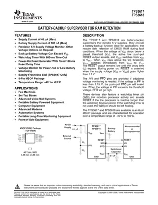
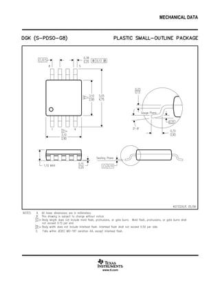
The document summarizes the TPS3617 and TPS3618 battery-backup supervisors. These ICs monitor a 5V supply and provide a battery-backup function to retain RAM data during power faults. When the VDD voltage drops below a threshold, the RESET output asserts and VOUT switches from VDD to VBAT. When VDD rises above the threshold, VOUT switches back to VDD. The RESET output remains low until the delay time expires. The ICs feature low power consumption, a watchdog timer, and power-on reset generator. They are available in an 8-pin MSOP package and operate from -40°C to 85°C.
Original Switching Voltage Regulators Mosfet N TK40E10N1 K40E10 100V 40A TO-9...AUTHELECTRONIC
Original Switching Voltage Regulators Mosfet N TK40E10N1 K40E10 100V 40A TO-92 New Toshiba Semiconductor
https://authelectronic.com/original-switching-voltage-regulators-mosfet-n-tk40e10n1-k40e10-100v-40a-to-92-new-toshiba-semiconductor
Sony 0.71 inch AMOLED 1920x1080 OLED Display HD-MI Board Available USB Driver...Shawn Lee
1. Description
The ECX335AF is a 1.8 cm (type 0.71) diagonal, 1920(RGB) × 1080 dots active-matrix color OLED panel module using single crystal silicon transistors. This panel incorporates panel driver and logic driver and realizes small size, light weight, and high definition.
(Applications: View finders, head-mounted displays, very small monitors, etc.)
2. Features
◆ Small size high definition type 0.70 display dots: 1920 (RGB)×1080 = 6.22 M dots
◆ High contrast
◆ Wide color reproduction range
◆ High-speed response
◆ Thin type and light weight
◆ Power saving function
◆ Up/down and/or right/left inverse display function
◆ Orbit supported
Whatsapp: +86 18566294218
Email: shawn.lee@panoxdisplay.com
OLED/LCD supplier: www.panoxdisplay.com
Wearable 1.78 inch Square AMOLED Display 368*448 For Smart Watch Bracelet Scr...Shawn Lee
1.78 inch AMOLED is a low power consumption AMOLED with 368x448 resolution and MIPI/SPI interface.
The IC mode is RM69090 which is widely used in wearable AMOLED displays such as 1.39" AMOLED.
It has an integrated CTP with TMA525C touch IC.
Application: Wearable, Medical equipment
Whatsapp: +86 18566294218
Email: shawn.lee@panoxdisplay.com
OLED/LCD supplier: www.panoxdisplay.com
Công ty cổ phần Hạo Phương xin gửi đến quý khách hàng Catalog relay Idec gồm đầy đủ các thông tin cơ bản như: thông số kỹ thuật, kích thước, sơ đồ dây….
Tham khảo các dòng Relay Idec thông dụng tại thị trường Việt Nam: RU4S, RU2S, RY4S, RM2S, RJ1S,….
Thiết kế của Relay Idec tinh tế đến từng chi tiết, sản phẩm luôn đảm bảo độ chính xác và chất lượng. Các ổ cắm dễ dàng sử dụng và có thể gắn trên Din rail, panel hoặc PCB.
Công ty TNHH Hạo Phương là đối tác phân phối các thiết bị điện công nghiệp của hãng IDEC IZUMI: đèn báo nút nhấn, relay, timer, PLC, màn hình idec...www.haophuong.com
ICL7660 Monolithic CMOS Voltage ConvertersGeorgage Zim
ICL7660 and ICL7660A contain all the necessary circuitry to complete a negative voltage converter, with the exception of 2 external capacitors which may be inexpensive 10μF polarized electrolytic types. Please visit for more information http://www.intersil.com/en/products/power-management/isolated-power/charge-pumps/ICL7660.html
Trailblazing in the Wilderness of Data ManagementStephanie Wright
Presentation to Montana State University faculty and librarians. Suggestions for services and collaborations for consideration in development of a new data management program.
Original N-channel 650 V 0.230 Ohm 12 A MDmesh V Power MOSFET in DPAK DPAK ST...AUTHELECTRONIC
Original N-channel 650 V 0.230 Ohm 12 A MDmesh V Power MOSFET in DPAK DPAK STF16N65M5 16N65M5 16N65 710V 12A TO-220FP New STMicroelectronics
https://authelectronic.com/original-n-channel-650-v-0-230-ohm-12-a-mdmesh-v-power-mosfet-in-dpak-dpak-stf16n65m5-16n65m5-16n65-710v-12a-to-220fp-new-stmicroelectronics
Using recycled concrete aggregates (RCA) for pavements is crucial to achieving sustainability. Implementing RCA for new pavement can minimize carbon footprint, conserve natural resources, reduce harmful emissions, and lower life cycle costs. Compared to natural aggregate (NA), RCA pavement has fewer comprehensive studies and sustainability assessments.
We have compiled the most important slides from each speaker's presentation. This year’s compilation, available for free, captures the key insights and contributions shared during the DfMAy 2024 conference.
NUMERICAL SIMULATIONS OF HEAT AND MASS TRANSFER IN CONDENSING HEAT EXCHANGERS...ssuser7dcef0
Power plants release a large amount of water vapor into the
atmosphere through the stack. The flue gas can be a potential
source for obtaining much needed cooling water for a power
plant. If a power plant could recover and reuse a portion of this
moisture, it could reduce its total cooling water intake
requirement. One of the most practical way to recover water
from flue gas is to use a condensing heat exchanger. The power
plant could also recover latent heat due to condensation as well
as sensible heat due to lowering the flue gas exit temperature.
Additionally, harmful acids released from the stack can be
reduced in a condensing heat exchanger by acid condensation. reduced in a condensing heat exchanger by acid condensation.
Condensation of vapors in flue gas is a complicated
phenomenon since heat and mass transfer of water vapor and
various acids simultaneously occur in the presence of noncondensable
gases such as nitrogen and oxygen. Design of a
condenser depends on the knowledge and understanding of the
heat and mass transfer processes. A computer program for
numerical simulations of water (H2O) and sulfuric acid (H2SO4)
condensation in a flue gas condensing heat exchanger was
developed using MATLAB. Governing equations based on
mass and energy balances for the system were derived to
predict variables such as flue gas exit temperature, cooling
water outlet temperature, mole fraction and condensation rates
of water and sulfuric acid vapors. The equations were solved
using an iterative solution technique with calculations of heat
and mass transfer coefficients and physical properties.
Welcome to WIPAC Monthly the magazine brought to you by the LinkedIn Group Water Industry Process Automation & Control.
In this month's edition, along with this month's industry news to celebrate the 13 years since the group was created we have articles including
A case study of the used of Advanced Process Control at the Wastewater Treatment works at Lleida in Spain
A look back on an article on smart wastewater networks in order to see how the industry has measured up in the interim around the adoption of Digital Transformation in the Water Industry.
Saudi Arabia stands as a titan in the global energy landscape, renowned for its abundant oil and gas resources. It's the largest exporter of petroleum and holds some of the world's most significant reserves. Let's delve into the top 10 oil and gas projects shaping Saudi Arabia's energy future in 2024.
Forklift Classes Overview by Intella PartsIntella Parts
Discover the different forklift classes and their specific applications. Learn how to choose the right forklift for your needs to ensure safety, efficiency, and compliance in your operations.
For more technical information, visit our website https://intellaparts.com
2. www.ti.com
ABSOLUTE MAXIMUM RATINGS
DISSIPATION RATING TABLE
TPS3617
TPS3618
SLVS339D–DECEMBER 2000–REVISED DECEMBER 2006
This integrated circuit can be damaged by ESD. Texas Instruments recommends that all integrated circuits be handled with
appropriate precautions. Failure to observe proper handling and installation procedures can cause damage.
ESD damage can range from subtle performance degradation to complete device failure. Precision integrated circuits may be
more susceptible to damage because very small parametric changes could cause the device not to meet its published
specifications.
PACKAGE INFORMATION(1)
NOMINAL SPECIFIED
SUPPLY THRESHOLD TEMPERATURE PACKAGE ORDERING TRANSPORT MEDIA,
PRODUCT VOLTAGE VOLTAGE (VIT)(2) RANGE MARKING NUMBER QUANTITY
TPS3617-50DGK Tube, 80
TPS3617-50 ASD
TPS3617-50DGKR Tape and Reel, 2500
5V 4.55V –40°C to +125°C
TPS3618-50DGKT Tape and Reel, 250
TPS3618-50 ANK
TPS3618-50DGKR Tape and Reel, 2500
(1) For the most current package and ordering information, see the Package Option Addendum at the end of this data sheet, or refer to our
web site at www.ti.com.
(2) For other threshold votages, contact the local TI sales office for availability and lead time.
over operating free-air temperature (unless otherwise noted)(1)
TPS3617, TPS3618 UNIT
Input voltage range, VDD –0.3 to 7 V
Input voltage range, PFI pin –0.3 to (VDD + 0.3) V
WDI pin –0.3 to (VDD + 0.3) V
Continuous output current at VOUT, IO 400 mA
All other pins, IO ±10 mA
Operating junction temperature range, TJ
(2) –40 to +85 °C
Storage temperature range, TSTG –65 to +150 °C
Lead temperature soldering 1,6 mm (1/16 inch) from case for 10 seconds +260 °C
Continuous total power dissipation See Dissipation Rating Table
(1) Stresses beyond those listed under Absolute Maximum Ratings may cause permanent damage to the device. These are stress ratings
only, and functional operation of the device at these or any other conditions beyond those indicated under Recommended Operating
Conditions is not implied. Exposure to absolute-maximum-rated conditions for extended periods may affect device reliability.
(2) Due to the low dissipated power in this device, it is assumed that TJ = TA.
TA ≤ +25°C DERATING FACTOR TA = +70°C TA = +85°C
PACKAGE POWER RATING ABOVE TA = +25°C POWER RATING POWER RATING
DGK 470 mW 3.76 mW/°C 301 mW 241 mW
2 Submit Documentation Feedback
3. www.ti.com
ELECTRICAL CHARACTERISTICS
TPS3617
TPS3618
SLVS339D–DECEMBER 2000–REVISED DECEMBER 2006
1.65 V ≤ VDD≤ 5.5 V, RLRESET = 1 MΩ, CLRESET = 50 pF, over operating temperature range (TJ = –40°C to +85°C), unless
otherwise noted. Typical values are at TJ = +25°C.
PARAMETER TEST CONDITIONS MIN TYP MAX UNIT
VDD Input supply range 1.65 5.5 V
VOUT = VDD 40
IDD VDD supply current µA
VOUT = VBAT 40
VBAT Battery supply range 1.5 5.5 V
VOUT = VDD –0.1 0.1
IBAT VBAT supply current µ A
VOUT = VBAT 0.5
Slew rate at VDD or VBAT 1 V/µs
VI Input volrage, any input 0 VDD + 0.3 V
VDD = 1.8 V, IOH = –400 µA VDD – 0.2
RESET VDD = 3.3 V, IOH = –2 mA,
VDD – 0.4
VDD = 5 V, IOH = –3 mA
VOH High-level output voltage V
VDD = 1.8 V, IOH = –20 µA VDD – 0.3
PFO VDD = 3.3 V, IOH = –80 µA,
VDD – 0.4
VDD = 5 V, IOH = –120 µA
VDD = 1.8 V, IOL = 400 µA 0.2
VOL Low-level output voltage RESET PFO VVDD = 3.3 V, IOL = 2 mA,
0.4
VDD = 5 V, IOL = 3 mA
VBAT > 1.1 V, or VDD > 1.1 V,
VRES Power-up reset voltage (1) 0.4 V
IOL = 20 µA
IO = 8.5 mA,VDD = 1.8 V, VBAT = 0 V VDD – 0.050
Normal mode IO = 125 mA,VDD = 3.3 V, VBAT = 0 V VDD – 0.150
VOUT IO = 200 mA,VDD = 5 V, VBAT = 0 V VDD – 0.200 V
IO = 0.5 mA,VBAT = 1.5 V, VDD = 0 V VBAT – 0.200
Battery-backup mode
IO = 7.5 mA,VBAT = 3.3 V, VDD = 0 V VBAT – 0.113
VDD to VOUT on-resistance VDD = 5 V 0.6 1
RDS(on) Ω
VBAT to VOUT on-resistance VBAT = 3.3 V 8 15
IO Continuous output current at VOUT 300 mA
VIT TPS3617-50 4.46 4.55 VNegative-going input
TA = –40°C to +85°C
threshold voltage (2)
VPFI PFI 1.13 1.15 1.17 V
1.65 V < VIT < 2.5 V 20
VIT hysteresis 2.5 V < VIT < 3.5 V 40
VHYS 3.5 V < VIT < 5.5 V 60 mV
PFI hysteresis 12
VBSW hysteresis (3) VDD = 1.8 V 55
VIH WDI high-level input voltage 0.7 x VDD
VIL WDI low-level input voltage 0.3 x VDD
IIH WDI high-level input current (4) WDI = VDD = 5 V 150 µA
IIL WDI low-level input current (4) WDI = 0 V, VDD = 5 V –150 µA
WDI input transition rise and fall rate, ∆t/∆V 100 ns/V
II PFI input current PFI voltage < VDD –25 25 nA
PFO = 0 V, VDD = 1.8 V –0.3
IOS PFO short-circuit current PFO = 0 V, VDD = 3.3 V –1.1 mA
PFO = 0 V, VDD = 5 V –2.4
(1) The lowest supply voltage at which RESET becomes active. tr, VDD ≥ 15 µs/V.
(2) To ensure the best stability of the threshold voltage, a bypass capacitor (ceramic, 0.1 µF) should be placed near the supply terminals.
(3) For VDD < 1.6 V, VOUT switches to VBAT regardless of VBAT.
(4) For details on how to optimize current consumption when using WDI, refer to the Watchdog section of this data sheet.
3Submit Documentation Feedback
4. www.ti.com
VIT
VBAT
VDD
VOUT
RESET
td
t
t
t
td
TPS3617
TPS3618
SLVS339D–DECEMBER 2000–REVISED DECEMBER 2006
ELECTRICAL CHARACTERISTICS (continued)
1.65 V ≤ VDD≤ 5.5 V, RLRESET = 1 MΩ, CLRESET = 50 pF, over operating temperature range (TJ = –40°C to +85°C), unless
otherwise noted. Typical values are at TJ = +25°C.
PARAMETER TEST CONDITIONS MIN TYP MAX UNIT
Ci Input capacitance, any input VI = 0 V to 5 V 5 pF
VDD VIH = VIT + 0.2 V, VIL = VIT– 0.2 V 6 µs
tw Pulse Width VDD > VIT + 0.2 V, VIL = 0.3 x VDD,
WDI 100 ns
VIH = 0.7 x VDD
td VDD ≥ VIT + 0.2 V,
Delay time 60 100 140 ms
See timing diagram
t(tout) VDD > VIT + 0.2 V,
Watchdog time-out 0.48 0.8 1.12 s
See timing diagram
VIL = VIT– 0.2 V,
VDD to RESET 2 5
VIH = VIT + 0.2 VPropagation (delay) time,
tPHL µs
high-to-low-level output VIL = VPFI– 0.2 V,
PFI to PFO 3 5
VIH = VPFI + 0.2 V
Transition time VDD to VBAT 3 µs
TIMING DIAGRAM
Table 1. FUNCTION TABLE
VDD > VIT VDD > VBAT VOUT RESET
0 0 VBAT 0
0 1 VDD 0
1 0 VDD 1
1 1 VDD 1
4 Submit Documentation Feedback
5. www.ti.com
Switch
Control_
+
RESET
Logic
+
Timer_
+
Reference
Voltage
or 1.15 V
VOUT
RESET
VBAT
VDD
PFI
TPS3617
GND
Watchdog
Logic
+
Control
Oscillator
PFO
+
−
Transition
Detector
WDI
40 kΩ
TPS3618
TPS3617
TPS3618
SLVS339D–DECEMBER 2000–REVISED DECEMBER 2006
Table 2. PFO FUNCTION
TABLE
PFI > VPFI PFO
0 0
1 1
CONDITION: VDD > VDD(MIN)
Table 3. TERMINAL FUNCTIONS
TERMINAL
NAME NO. I/O DESCRIPTION
GND 3 I Ground
PFI 4 I Power-fail comparator input
PFO 5 O Power-fail comparator output; asserts low when PFI < 1.15 V
RESET 7 O Active-low push-pull reset output
VBAT 8 I Backup-battery input
VDD 2 I Input supply voltage
VOUT 1 O Supply output
WDI 6 I Watchdog input. Should be left floating if not used.
FUNCTIONAL BLOCK DIAGRAM
5Submit Documentation Feedback
6. www.ti.com
TYPICAL CHARACTERISTICS
TABLE OF GRAPHS
5
7.5
10
12.5
15
17.5
20
2.5 4.5 6.5 8.5 10.5 12.5 14.5
−StaticDrain-SourceOn-StateResistance−
IO − Output Current − mA
rDS(on)Ω
TA = 85°C
VBAT = 3.3 V
TA = 25°C
TA = 0°C
TA = −40°C
500
600
700
800
900
1000
50 75 100 125 150 175 200
TA = 85°C
TA = 25°C
TA = 0°C
TA = −40°C
−StaticDrain-SourceOn-StateResistance−m
VDD = 3.3 V
VBAT = GND
IO − Output Current − mA
rDS(on)Ω
TPS3617
TPS3618
SLVS339D–DECEMBER 2000–REVISED DECEMBER 2006
FIGURE
Static drain-source on-state resistance (VDD to VOUT) vs Output current 3
rDS(on)
Static drain-source on-state resistance (VBAT to VOUT) vs Output current 4
IDD Supply current vs Supply voltage 5
VIT Input threshold voltage at RESET vs Free-air temperature 6
High-level output voltage at RESET 7, 8
VOH vs High-level output current
High-level output voltage at PFO 9, 10
VOL Low-level output voltage at RESET vs Low-level output current 11, 12
Minimum pulse duration at VDD vs Threshold voltage overdrive at VDD 13
Minimum pulse duration at PFI vs Threshold voltage overdrive at PFI 14
STATIC DRAIN-SOURCE ON-STATE RESISTANCE STATIC DRAIN-SOURCE ON-STATE RESISTANCE
(VDD to VOUT) (VBAT to VOUT)
vs vs
OUTPUT CURRENT OUTPUT CURRENT
Figure 1. Figure 2.
6 Submit Documentation Feedback
7. www.ti.com
0.995
0.996
0.997
0.998
0.999
1
1.001
−40 −30 −20 −10 0 10 20 30 40 50 60 70 80
TA − Free-Air Temperature − °C
−InputThresholdVoltageatRESET−VVIT
0
5
10
15
20
25
30
0 1 2 3 4 5 6
TA = −40°C
TA = 25°C
TA = 85°C
TA = 0°C
−SupplyCurrent−IDDAµ
VDD − Supply Voltage − V
VBAT Mode
VBAT = 2.6 V
VDD Mode
VBAT = GNDor
0
1
2
3
4
5
6
−35 −30 −25 −20 −15 −10 −5 0
TA = −40°C
TA = 85°C
TA = 0°C
TA = 25°C
−High-LevelOutputVoltageatRESET−VVOH
IOH − High-Level Output Current − mA
VDD = 5 V
VBAT = GND
TPS3617
TPS3618
SLVS339D–DECEMBER 2000–REVISED DECEMBER 2006
SUPPLY CURRENT INPUT THRESHOLD VOLTAGE AT RESET
vs vs
SUPPLE VOLTAGE FREE-AIR TEMPERATURE
Figure 3. Figure 4.
HIGH-LEVEL OUTPUT VOLTAGE AT RESET
vs
HIGH-LEVEL OUTPUT CURRENT
Figure 5.
7Submit Documentation Feedback
8. www.ti.com
0
1
2
3
4
5
6
−2.5 −2 −1.5 −1 −0.5 0
TA = −40°C
TA = 25°C
TA = 85°C
TA = 0°C
−High-LevelOutputVoltageatPFO−VVOH
IOH − High-Level Output Current − mA
VDD = 5.5 V
PFI = 1.4 V
VBAT = GND
4.5
4.6
4.7
4.8
4.9
5
5.1
−5 −4.5 −4 −3.5 −3 −2.5 −2 −1.5 −1 −0.5 0
TA = −40°C
TA = 25°C
TA = 85°C
TA = 0°C
IOH − High-Level Output Current − mA
VDD = 5 V
VBAT = GND
Expanded View
−High-LevelOutputVoltageatRESET−VVOH
0
0.5
1
1.5
2
2.5
3
3.5
0 5 10 15 20 25
TA = 25°C
TA = 85°C
TA = 0°C
TA = −40°C
−Low-LevelOutputVoltageatRESET−VVOL
IOL − Low-Level Output Current − mA
VDD = 3.3 V
VBAT = GND
5.10
5.15
5.20
5.25
5.30
5.35
5.40
5.45
5.50
5.55
−200 −180−160−140 −120−100 −80 −60 −40 −20 0
TA = −40°C
TA = 25°C
TA = 85°C
TA = 0°C
IOH − High-Level Output Current − µA
VDD = 5.5 V
PFI = 1.4 V
VBAT = GND
Expanded View
−High-LevelOutputVoltageatPFO−VVOH
TPS3617
TPS3618
SLVS339D–DECEMBER 2000–REVISED DECEMBER 2006
HIGH-LEVEL OUTPUT VOLTAGE AT RESET HIGH-LEVEL OUTPUT VOLTAGE AT PFO
vs vs
HIGH-LEVEL OUTPUT CURRENT HIGH-LEVEL OUTPUT CURRENT
Figure 6. Figure 7.
HIGH-LEVEL OUTPUT VOLTAGE AT PFO LOW-LEVEL OUTPUT VOLTAGE AT RESET
vs vs
HIGH-LEVEL OUTPUT CURRENT LOW-LEVEL OUTPUT CURRENT
Figure 8. Figure 9.
8 Submit Documentation Feedback
9. www.ti.com
0
100
200
300
400
500
0 1 2 3 4 5
TA = −40°C
TA = 25°C
TA = 85°C
TA = 0°C
−Low-LevelOutputVoltageatRESET−mVVOL
IOL − Low-Level Output Current − mA
VDD = 3.3 V
VBAT = GND
Expanded View
0
1
2
3
4
5
6
7
8
9
10
0 0.1 0.2 0.3 0.4 0.5 0.6 0.7 0.8 0.9
MinimumPulseDurationat−VDD Threshold Voltage Overdrive at VDD − V
1
sµ
0.6
1
1.4
1.8
2.2
2.6
3
3.4
3.8
4.2
4.6
5
0 0.1 0.2 0.3 0.4 0.5 0.6 0.7 0.8 0.9 1
MinimumPulseDurationatPFI−
Threshold Voltage Overdrive at PFI − V
VDD = 1.65 V
sµ
TPS3617
TPS3618
SLVS339D–DECEMBER 2000–REVISED DECEMBER 2006
LOW-LEVEL OUTPUT VOLTAGE AT RESET MINIMUM PULSE DURATION AT VDD
vs vs
LOW-LEVEL OUTPUT CURRENT THRESHOLD VOLTAGE OVERDRIVE AT VDD
Figure 10. Figure 11.
MINIMUM PULSE DURATION AT PFI
vs
THRESHOLD VOLTAGE OVERDRIVE AT PFI
Figure 12.
9Submit Documentation Feedback
10. www.ti.com
DETAILED DESCRIPTION
BATTERY FRESHNESS SEAL (TPS3617 Only)
POWER-FAIL COMPARATOR (PFI AND PFO)
WATCHDOG
VIT
WDI
RESET
td td
t(tout)
VOUT
td
Undefined
TPS3617
TPS3618
SLVS339D–DECEMBER 2000–REVISED DECEMBER 2006
The battery freshness seal of the TPS3617 family disconnects the backup battery from the internal circuitry until
it is needed. This ensures that the backup battery connected to VBAT should be fresh when the final product is
put to use. The following steps explain how to enable the freshness seal mode:
1. Connect VBAT (VBAT > VBAT(min)).
2. Ground PFO.
3. Connect PFI to VDD (PFI = VDD).
4. Connect VDD to power supply (VDD > VIT) and keep connected for 5 ms < t < 35 ms.
The battery freshness seal mode is disabled by the positive-going edge of RESET when VDD is applied.
An additional comparator monitors voltages other than the nominal supply voltage. The power-fail-input (PFI)
can be compared with an internal voltage reference of 1.15 V. If the input voltage falls below the power-fail
threshold (V(PFI)) of 1.15 V typical, the power-fail output (PFO) goes low. If it goes above V(PFI) plus about 12-mV
hysteresis, the output returns to high. By connecting two external resistors it is possible to supervise any
voltages above V(PFI). The sum of both resistors should be about 1 MΩ, to minimize power consumption and
also to ensure that the current in the PFI pin can be neglected compared with the current through the resistor
network. The tolerance of the external resistors should be not more than 1% to ensure minimal variation of the
sensed voltage. If the power-fail comparator is unused, connect PFI to ground and leave the PFO unconnected.
In a microprocessor- or DSP-based system, it is not only important to supervise the supply voltage, it is also
important to ensure correct program execution. The task of a watchdog is to ensure that the program is not
stalled in an indefinite loop. The microprocessor, microcontroller, or DSP has to toggle the watchdog input within
0.8 s typically, to avoid a timeout from occurring. Either a low-to-high or a high-to-low transition resets the
internal watchdog timer. If the input is unconnected, the watchdog is disabled and should be retriggered
internally. See Figure 13 for the watchdog timing diagram.
Figure 13. Watchdog Timing
10 Submit Documentation Feedback
11. www.ti.com
SAVING CURRENT WHILE USING THE WATCHDOG
BACKUP-BATTERY SWITCHOVER
VDD – Mode
VBAT – Mode
VBSW Hysteresis
VIT Hysteresis
VBAT – Backup-Battery Supply Voltage
–NormalSupplyVoltageVDD
Undefined
TPS3617
TPS3618
SLVS339D–DECEMBER 2000–REVISED DECEMBER 2006
DETAILED DESCRIPTION (continued)
The watchdog input is internally driven low during the first 7/8 of the watchdog time-out period, then momentarily
pulses high, resetting the watchdog counter. For minimum watchdog input current (minimum overall power
consumption), leave WDI low for the majority of the watchdog time-out period, pulsing it low-high-low once within
7/8 of the watchdog time-out period to reset the watchdog timer. If instead, WDI is externally driven high for the
majority of the time-out period, a current of e.g. 5.0 V/40 kΩ ≈ 125 µA can flow into WDI.
In case of a brownout or power failure, it may be necessary to preserve the contents of RAM. If a backup battery
is installed at VBAT, the device automatically switches the connected RAM to backup power when VDD fails. In
order to allow the backup battery (e.g., a 3.6-V lithium cell) to have a higher voltage than VDD, these supervisors
should not connect VBAT to VOUT when VBAT is greater than VDD. VBAT only connects to VOUT (through a 15-Ω
switch) when VDD falls below VIT and VBAT is greater than VDD. When VDD recovers, switchover is deferred either
until VDD crosses VBAT, or until VDD rises above the reset threshold VIT. VOUT connects to VDD through a 1-Ω
(max) PMOS switch when VDD crosses the reset threshold.
FUNCTION TABLE
VDD > VBAT VDD > VIT VOUT
1 1 VDD
1 0 VDD
0 1 VDD
0 0 VBAT
Figure 14. VDD – VBAT Switchover
11Submit Documentation Feedback
12. PACKAGE OPTION ADDENDUM
www.ti.com 10-Jun-2014
Addendum-Page 1
PACKAGING INFORMATION
Orderable Device Status
(1)
Package Type Package
Drawing
Pins Package
Qty
Eco Plan
(2)
Lead/Ball Finish
(6)
MSL Peak Temp
(3)
Op Temp (°C) Device Marking
(4/5)
Samples
TPS3617-50DGK ACTIVE VSSOP DGK 8 80 Green (RoHS
& no Sb/Br)
CU NIPDAU Level-1-260C-UNLIM -40 to 85 ASD
TPS3617-50DGKG4 ACTIVE VSSOP DGK 8 80 Green (RoHS
& no Sb/Br)
CU NIPDAU Level-1-260C-UNLIM -40 to 85 ASD
TPS3617-50DGKR ACTIVE VSSOP DGK 8 2500 Green (RoHS
& no Sb/Br)
CU NIPDAU Level-1-260C-UNLIM -40 to 85 ASD
TPS3618-50DGKT ACTIVE VSSOP DGK 8 250 Green (RoHS
& no Sb/Br)
CU NIPDAU Level-1-260C-UNLIM -40 to 125 ANK
(1)
The marketing status values are defined as follows:
ACTIVE: Product device recommended for new designs.
LIFEBUY: TI has announced that the device will be discontinued, and a lifetime-buy period is in effect.
NRND: Not recommended for new designs. Device is in production to support existing customers, but TI does not recommend using this part in a new design.
PREVIEW: Device has been announced but is not in production. Samples may or may not be available.
OBSOLETE: TI has discontinued the production of the device.
(2)
Eco Plan - The planned eco-friendly classification: Pb-Free (RoHS), Pb-Free (RoHS Exempt), or Green (RoHS & no Sb/Br) - please check http://www.ti.com/productcontent for the latest availability
information and additional product content details.
TBD: The Pb-Free/Green conversion plan has not been defined.
Pb-Free (RoHS): TI's terms "Lead-Free" or "Pb-Free" mean semiconductor products that are compatible with the current RoHS requirements for all 6 substances, including the requirement that
lead not exceed 0.1% by weight in homogeneous materials. Where designed to be soldered at high temperatures, TI Pb-Free products are suitable for use in specified lead-free processes.
Pb-Free (RoHS Exempt): This component has a RoHS exemption for either 1) lead-based flip-chip solder bumps used between the die and package, or 2) lead-based die adhesive used between
the die and leadframe. The component is otherwise considered Pb-Free (RoHS compatible) as defined above.
Green (RoHS & no Sb/Br): TI defines "Green" to mean Pb-Free (RoHS compatible), and free of Bromine (Br) and Antimony (Sb) based flame retardants (Br or Sb do not exceed 0.1% by weight
in homogeneous material)
(3)
MSL, Peak Temp. - The Moisture Sensitivity Level rating according to the JEDEC industry standard classifications, and peak solder temperature.
(4)
There may be additional marking, which relates to the logo, the lot trace code information, or the environmental category on the device.
(5)
Multiple Device Markings will be inside parentheses. Only one Device Marking contained in parentheses and separated by a "~" will appear on a device. If a line is indented then it is a continuation
of the previous line and the two combined represent the entire Device Marking for that device.
(6)
Lead/Ball Finish - Orderable Devices may have multiple material finish options. Finish options are separated by a vertical ruled line. Lead/Ball Finish values may wrap to two lines if the finish
value exceeds the maximum column width.
13. PACKAGE OPTION ADDENDUM
www.ti.com 10-Jun-2014
Addendum-Page 2
Important Information and Disclaimer:The information provided on this page represents TI's knowledge and belief as of the date that it is provided. TI bases its knowledge and belief on information
provided by third parties, and makes no representation or warranty as to the accuracy of such information. Efforts are underway to better integrate information from third parties. TI has taken and
continues to take reasonable steps to provide representative and accurate information but may not have conducted destructive testing or chemical analysis on incoming materials and chemicals.
TI and TI suppliers consider certain information to be proprietary, and thus CAS numbers and other limited information may not be available for release.
In no event shall TI's liability arising out of such information exceed the total purchase price of the TI part(s) at issue in this document sold by TI to Customer on an annual basis.