This document provides specifications for the TK40E10N1 MOSFET transistor. It includes:
1) Applications such as switching voltage regulators
2) Key features and specifications including low on-resistance, leakage current, enhancement mode voltage
3) Packaging and pinout information for the TO-220 package
4) Absolute maximum ratings and thermal/electrical characteristics
5) Testing and qualification information
Original N-Channel Mosfet TK10P60 TK10P60W TO-252 New ToshibaAUTHELECTRONIC
This document provides specifications for TK10P60W, an N-channel MOSFET silicon transistor. It includes:
1) Electrical characteristics such as on-resistance, threshold voltage, and maximum ratings.
2) Thermal characteristics such as thermal resistance.
3) Package and marking details.
4) Characteristics curves showing properties like current vs voltage.
Original N-Channel Mosfet TK9A20DA K9A20DA 9A20D 200V 8.5A TO-220 New ToshibaAUTHELECTRONIC
This document provides specifications for Toshiba's TK9A20DA N-Channel MOSFET transistor. Key details include:
- It has a low drain-source on-resistance of 0.26 ohms and is intended for use in switching voltage regulators.
- Electrical characteristics are provided, such as a threshold voltage of 1.5-3.5V and total gate charge of 14nC.
- Thermal characteristics include a channel-to-case thermal resistance of 4.16°C/W and channel-to-ambient thermal resistance of 62.5°C/W.
- Absolute maximum ratings and packaging/pinout diagrams are also included to help
Original N-Channel Mosfet TK12A65D K12A65D 12A65 TO-220F New ToshibaAUTHELECTRONIC
Original N-Channel Mosfet TK12A65D K12A65D 12A65 TO-220F New Toshiba
https://authelectronic.com/original-n-channel-mosfet-tk12a65d-k12a65d-12a65-to-220f-new-toshiba
This document provides specifications for the TK10A50D transistor made by Toshiba. Key details include:
- It is an N-channel MOSFET transistor suitable for switching regulator applications.
- Absolute maximum ratings include a drain-source voltage of 500V, drain current of 10A continuous and 40A pulse.
- Electrical characteristics include a typical drain-source on-resistance of 0.62Ω and forward transfer admittance of 5S.
- Thermal characteristics include a channel to case thermal resistance of 2.78°C/W.
Original N-Channel Mosfet FDPF33N25 33N25 TO-220 New FairChildAUTHELECTRONIC
This document provides information on the FDPF33N25250VN-Channel MOSFET from Fairchild Semiconductor. It is a 250V N-Channel MOSFET with low on-resistance of 0.094Ω and fast switching capabilities. It uses Fairchild's proprietary planar stripe DMOS technology to minimize resistance and maximize performance for applications such as high efficiency power supplies. Key specifications and performance characteristics are provided.
Original N Channel Mosfet 2SK3566 K3566 3566 2.5A 900V TO-220 NewAUTHELECTRONIC
Original N Channel Mosfet 2SK3566 K3566 3566 2.5A 900V TO-220 New
https://authelectronic.com/original-n-channel-mosfet-2sk3566-k3566-3566-2-5a-900v-to-220-new
Original N-Channel Mosfet STP65NF06 P65NF06 65A 60V TO-220 New STAUTHELECTRONIC
Original N-Channel Mosfet STP65NF06 P65NF06 65A 60V TO-220 New ST
https://authelectronic.com/original-n-channel-mosfet-stp65nf06-p65nf06-65a-60v-to-220-new
Original N-channel 600 V 0.160 Ω 19 A PowerFLAT™ 8x8 HV ultra low gate charge...AUTHELECTRONIC
This document provides information on the STL26NM60N N-channel 600 V, 0.160 Ω, 19 A PowerFLATTM 8x8 HV ultra low gate charge MDmeshTM II Power MOSFET, including:
- Key features such as being 100% avalanche tested and having low input capacitance and gate charge
- Applications in switching applications
- Description of the proprietary vertical and horizontal process technologies used to achieve extremely low on-resistance
- Electrical ratings, characteristics and switching performance curves
- Package mechanical data for the PowerFLATTM 8x8 HV package
This document provides specifications for the ACPL-C87B/C87A/C870 precision optically isolated voltage sensor. It includes:
- Key features such as high input impedance, wide operating temperature range, and small package size.
- Electrical specifications including gain accuracy of ±0.5% for the ACPL-C87B, input offset voltage, nonlinearity, and temperature drift.
- Recommended operating conditions and absolute maximum ratings.
- Safety and regulatory approval information for worldwide use.
Catalog Relay Idec
Beeteco.com là trang mua sắm trực tuyến thiết bị điện - Tự động hóa uy tín tại Việt Nam.
Chuyên cung cấp các thiết bị: Đèn báo nút nhấn, Relay, Timer, Contactor, MCCB ELCB, Biến tần, Van, Thiết bị cảm biến, phụ kiện tủ điện, .... Từ các thương hiệu hàng đầu trên thế giới.
www.beeteco.com @ Công ty TNHH TM KT ASTER
Số 7 Đại Lộ Độc Lập, KCN Sóng Thần 1, P. Dĩ An, Tx. Dĩ An, Bình Dương
www.facebook.com/beeteco
Tel: 0650 3617 012
DĐ: 0904 676 925
For more information, please feel free to visit the site at the following link: http://www.kynix.com/Detail/6239/IL711T-1E.html. You can choose Kynix as the first place and you can feel free to buy what you need in Kynix at the lower prices.
Original N-Channel Mosfet STS4DNF60L 4DF60L 60V 4A SOP-8 New STMicroelectronicsAUTHELECTRONIC
This document provides information on an N-channel 60V power MOSFET from STMicroelectronics called the STS4DNF60L. It has a maximum drain-source voltage of 60V, on-resistance of less than 0.055 ohms, and continuous drain current of 4A. The document includes electrical ratings and characteristics, test circuits, package mechanical data, and a revision history.
Catalogue Timer Idec
Beeteco.com là trang mua sắm trực tuyến thiết bị điện - Tự động hóa uy tín tại Việt Nam.
Chuyên cung cấp các thiết bị: Đèn báo nút nhấn, Relay, Timer, Contactor, MCCB ELCB, Biến tần, Van, Thiết bị cảm biến, phụ kiện tủ điện, .... Từ các thương hiệu hàng đầu trên thế giới.
www.beeteco.com @ Công ty TNHH TM KT ASTER
Số 7 Đại Lộ Độc Lập, KCN Sóng Thần 1, P. Dĩ An, Tx. Dĩ An, Bình Dương
www.facebook.com/beeteco
Tel: 0650 3617 012
DĐ: 0904 676 925
Original N Channel Mosfet FQPF12N60 12N60 12A 600V New FairchildAUTHELECTRONIC
Original N Channel Mosfet FQPF12N60 12N60 12A 600V New Fairchild
https://authelectronic.com/original-n-channel-mosfet-fqpf12n60-12n60-12a-600v-new-fairchild
Original N-Channel Mosfet STN2NF10 2NF10 N2NF10 2.4A 100V SOT-223 New STMicro...AUTHELECTRONIC
This document provides specifications for the STN2NF10 N-channel 100V MOSFET from STMicroelectronics. Key details include:
- The MOSFET has an on-resistance of 0.23Ω maximum and can handle continuous drain currents up to 2.4A.
- Electrical characteristics and ratings are provided in tables, along with test circuits and package mechanical data.
- Revision history shows the document was last updated in April 2007 with minor changes to figures and test conditions.
Original N Channel Mosfet 110N8F6 STP110N8F6 110A 80V TO-220 NewAUTHELECTRONIC
This document provides product information for the STP110N8F6 power MOSFET, including:
1. Electrical ratings and characteristics such as maximum voltage, current, and on-resistance.
2. Test circuits for evaluating switching times and diode recovery.
3. Package information for the TO-220 package including mechanical dimensions.
Original NPN Transistor FZT857 857 FZT 300V 3.5A SOT-223F NewAUTHELECTRONIC
This document provides information on the FZT857 300V NPN medium power transistor. Key details include:
- Electrical specifications such as a collector-emitter breakdown voltage of 300V, continuous collector current of 3.5A, and saturation voltage below 155mV at 1A.
- Thermal characteristics including a maximum power dissipation of 3W at an ambient temperature of 25°C and package details for the SOT223 package.
- Test conditions and typical electrical characteristics curves for parameters like current gain and saturation voltage over varying collector currents.
- Ordering information and product marking diagrams.
Original N-Channel Mosfet TK10P60 TK10P60W TO-252 New ToshibaAUTHELECTRONIC
This document provides specifications for TK10P60W, an N-channel MOSFET from Toshiba. It includes key electrical and thermal characteristics such as an on-resistance of 0.327 ohms, breakdown voltage of 600V, and thermal resistance of 1.57 degrees Celsius per watt. The MOSFET is packaged in a DPAK package and is intended for use in applications such as switching voltage regulators.
Original IGBT TK8A60DA K8A60 600V 7.5A TO-220F New ToshibaAUTHELECTRONIC
This document provides specifications for the TK8A60DA MOSFET transistor. It includes:
- Absolute maximum ratings for voltage, current, power and temperature.
- Electrical characteristics like threshold voltage, on resistance and capacitance.
- Thermal characteristics like thermal resistance.
- Safe operating area curves and avalanche energy ratings.
- Testing conditions and notes on using the transistor within specified limits to ensure reliability.
Original Transistor TK6A60D K6A60D 6A60D 6A 600V TO-220F New Toshiba Semicond...AUTHELECTRONIC
This document provides specifications for the TK6A60D MOSFET transistor made by Toshiba. It includes:
- Absolute maximum ratings for voltage, current, power and temperature.
- Electrical characteristics like threshold voltage, on-resistance, capacitance.
- Thermal characteristics such as thermal resistance.
- Graphs of characteristics like on-resistance over temperature and avalanche energy over initial channel temperature.
- Notes on single pulse and repetitive avalanche energy ratings, and restrictions on product use.
This document provides specifications for the TK15A60D silicon n-channel MOS field effect transistor made by Toshiba. Some key specifications include:
- Maximum drain-source voltage of 600V
- Typical on-resistance of 0.31 ohms
- Maximum drain current of 15A continuous, 60A pulse
- Enhancement mode with threshold voltage of 2.0-4.0V
It also provides detailed electrical characteristics, thermal characteristics, and safety considerations for using the transistor.
Original Mosfet P-Channel TJ20A10M3 J20A10M3 J20A10M 100V 10A TO-220 NewAUTHELECTRONIC
This document provides specifications for the TJ20A10M3 P-channel MOSFET transistor made by Toshiba. Some key specifications include a maximum drain-source voltage of -100V, typical drain-source on resistance of 63mΩ, and maximum drain cut-off current of -10μA. The document also provides charts showing electrical characteristics like drain current vs drain-source voltage under different conditions and maximum ratings for pulsed operations. Safety guidelines are provided to prevent unintended or unsafe uses of the transistor.
Original N Channel Transistor TK20A60U K20A60U K20A60 20A 600V TO220 Newauthelectroniccom
This document provides specifications for the TK20A60U field effect transistor made by Toshiba. Some key specifications include:
- Maximum drain-source voltage of 600V
- On-resistance as low as 0.165 ohms
- Forward transfer admittance as high as 12S
- Maximum drain cut-off current of 100uA
It also provides timing characteristics, thermal characteristics, and maximum ratings for the transistor. Notes provide important information on ensuring safe operation and derating for long term reliability.
Original N Channel Mosfet T5A50D K5A50D 5A50D TO-220 5A 500V New Toshiba(Repl...AUTHELECTRONIC
Original N Channel Mosfet T5A50D K5A50D 5A50D TO-220 5A 500V New Toshiba(Replacement K10A60D)
https://authelectronic.com/original-n-channel-mosfet-t5a50d-k5a50d-5a50d-to-220-5a-500v-new-toshiba-replacement-k10a60d
Original N-Channel Mosfet 2SK3484 3484 16A 100V TO-252 New Renesas ElectronicsAUTHELECTRONIC
This document provides specifications for the 2SK3484 N-channel MOS field effect transistor (MOSFET) including:
- Electrical characteristics such as on-state resistance, gate cut-off voltage, and input/output capacitances.
- Thermal characteristics such as thermal resistance and power dissipation derating curves.
- Switching characteristics such as turn-on/off delay times and rise/fall times.
- Package drawings and equivalent circuit diagram for the TO-251 and TO-252 packages.
Original Mosfet N-Channel SSM3K15FV OP SMD Code SOT-723 NewAUTHELECTRONIC
This document provides specifications for the Toshiba SSM3K15FV n-channel MOS field effect transistor. It has a maximum drain-source voltage of 30V, drain current of 100mA, and drain power dissipation of 150mW. Key characteristics include a typical gate threshold voltage of 0.8-1.5V and on-resistance of 4.0Ω maximum at 4V gate-source voltage and 7.0Ω maximum at 2.5V. Switching times are 50ns turn-on time and 180ns turn-off time. The document also outlines absolute maximum ratings and electrical characteristics.
Original Mosfet 047N08 FDP047N08 47N08 75V TO-220 New FairchildAUTHELECTRONIC
Original Mosfet 047N08 FDP047N08 47N08 75V TO-220 New Fairchild
https://authelectronic.com/original-mosfet-047n08-fdp047n08-47n08-75v-to-220-new-fairchild
Original MOSFET N-CHANNEL STP80NF70 80NF70 80N70 80A 70V New AUTHELECTRONIC
This document provides information on the STP80NF70 N-channel power MOSFET, including:
1. Electrical ratings and characteristics such as drain-source breakdown voltage, on-resistance, gate charge, and switching times.
2. Test circuits for evaluating electrical parameters.
3. Package mechanical data for the TO-220 package.
The DS1307 is a real-time clock with 56 bytes of battery-backed SRAM and an I2C serial interface. It keeps time in seconds, minutes, hours, date, month, and year formats with leap year compensation. The device operates from a primary power supply or backup battery. It enters a low-power mode when running from battery alone.
Orriginal N-Channel Mosfet K3564 3564 2SK3564 TO-220F New ToshibaAUTHELECTRONIC
This document provides specifications for the TOSHIBA 2SK3564 field effect transistor. It is a silicon n-channel MOS transistor intended for switching regulator applications. Key specifications include a low drain-source ON resistance of 3.7 ohms typical, a high forward transfer admittance of 2.6 Siemens typical, and a low leakage current of 100 microamps maximum. Absolute maximum ratings and electrical characteristics are provided along with typical performance curves.
Original P-Channel Mosfet TPC8107 13A 30V SOP-8 NewAUTHELECTRONIC
This document provides specifications for the TPC8107 P-channel MOSFET transistor made by Toshiba. Key details include:
- It is suitable for applications such as notebook PCs, portable equipment, and lithium ion battery applications.
- It has a small footprint due to a small, thin package and low drain-source on resistance of 5.5 mOhms typical.
- Maximum ratings include a drain-source voltage of -30V, drain current of -13A DC and -52A pulse, and channel temperature of 150°C.
Original N-channel 650 V 0.230 Ohm 12 A MDmesh V Power MOSFET in DPAK DPAK ST...AUTHELECTRONIC
Original N-channel 650 V 0.230 Ohm 12 A MDmesh V Power MOSFET in DPAK DPAK STF16N65M5 16N65M5 16N65 710V 12A TO-220FP New STMicroelectronics
https://authelectronic.com/original-n-channel-650-v-0-230-ohm-12-a-mdmesh-v-power-mosfet-in-dpak-dpak-stf16n65m5-16n65m5-16n65-710v-12a-to-220fp-new-stmicroelectronics
Similar to Original Switching Voltage Regulators Mosfet N TK40E10N1 K40E10 100V 40A TO-92 New Toshiba Semiconductor (20)
Original Power Supply IC LNK632DG LNK632 632 SOP-7 NewAUTHELECTRONIC
The LNK632DG is an energy efficient constant voltage/constant current switcher for adapters and chargers. It dramatically simplifies CV converter designs by eliminating secondary control circuitry and compensation components. Some key features include auto-restart protection, hysteretic thermal shutdown, tight output regulation that compensates for cable voltage drops and temperature variations, and high efficiency down to light loads. It is well-suited for charger applications like cell phones, PDAs, and MP3 players.
The document summarizes an low-profile relay model called G5RL that is suitable for various applications. It has several models including standard, low noise, high inrush, and high capacity. Key specifications include a height of 15.7mm, 8mm creepage distance, 10kV impulse withstand voltage. It provides information on ordering, ratings for coils and contacts, characteristics, dimensions, and engineering data.
Original Transition-Mode PFC Controller IC LD7591GS 7591 SOP-8 New LeadtrendAUTHELECTRONIC
This document provides information about the LD7591 transition-mode PFC controller, including:
- It is a voltage mode PFC controller that operates in transition mode with protections like OVP, OCP, and brown-in protection.
- It has features like low startup current, over voltage protection, open feedback protection, disable function, and integrated current sensing.
- Typical applications include adapters over 65W, open frame switching power supplies, LCD TV power supplies, and LED power supplies.
Original NPN Darlington Transistor MC1413DR2G 1413DR2G NCV1413BDG 1413BDG 141...AUTHELECTRONIC
The document describes a high voltage, high current Darlington transistor array that is well-suited for driving lamps, relays, or printer hammers. It has 7 NPN Darlington connected transistors with a high breakdown voltage and internal suppression diodes to ensure safety with inductive loads. It can drive incandescent lamps with peak inrush currents up to 500mA per transistor.
Original EEPROM IC BR93L76RFJ 93L76 RL76 SOP-8 New RohmAUTHELECTRONIC
This document provides important safety information regarding the intended use of ROHM products. It states that the products are designed for ordinary electronic equipment but should not be used in applications requiring extremely high reliability where malfunctions could directly endanger human life, such as medical devices. It also notes the products are not designed with antiradiation properties and certain exports may require controls under Japanese law. Contact information is provided for sales representatives.
Original Advanced IGBT/Mosfet Driver TD350E 350E SOP-14 New ST MicroelectronicsAUTHELECTRONIC
This document provides information on an advanced IGBT/MOSFET gate driver called the TD350E, including its key features, applications, description, and specifications. The TD350E is designed for applications such as inverters, motor control, and UPS systems. It provides 1.5A/2.3A gate drive, active Miller clamping, two-level turn-off protection, desaturation detection, and fault status output. Electrical characteristics and timing diagrams are included to specify the device's performance.
Original N-Channel Mosfet 2SK3562 3562 TO-220 New ToshibaAUTHELECTRONIC
This document provides specifications and performance characteristics for the Toshiba 2SK3562 N-channel MOSFET transistor. Key details include:
- It is an enhancement mode transistor intended for switching regulator applications with low on-resistance of 0.9 ohms and forward transfer admittance of 5.0S.
- Maximum ratings include a drain-source voltage of 600V, drain current of 6A continuous or 24A pulse, and drain power dissipation of 40W.
- Electrical characteristics at 25C include a gate threshold voltage of 2.0-4.0V, on-resistance of 0.9-1.25 ohms, and input/output capacit
Original N-Channel Mosfet IRFB4020PBF 4020 TO-220-3 New International RectifierAUTHELECTRONIC
This document provides specifications for a digital audio MOSFET designed for use in class D audio amplifier applications. The MOSFET has been optimized to achieve low on-resistance, gate charge, and reverse recovery charge for improved efficiency, total harmonic distortion, and electromagnetic interference. Additional features include a 175°C operating temperature and repetitive avalanche capability making it robust and reliable for audio amplifiers. Tables and graphs provide electrical characteristics and performance metrics.
Original Logic IC SN74LVC14A SN54LVC14A 74LVC14A 54LVC14A SOP-14 New Texas In...AUTHELECTRONIC
The document provides information on the SN54LVC14A and SN74LVC14A hex Schmitt-trigger inverter integrated circuits. It describes their operating voltage ranges from 1.65V to 3.6V, maximum propagation delay of 6.4ns at 3.3V, ESD protection exceeding 2000V human-body and 200V machine models, and thermal characteristics with package impedance ranging from 47°C/W to 127°C/W. Ordering information and packaging details are provided for various operating temperature ranges from -55°C to 125°C. Electrical characteristics like input thresholds, output voltages, input and output currents, and input capacitance are specified over operating conditions.
Original High Voltage Isolation IC ACS710T KLA-12CB 710T SOP-16 NewAUTHELECTRONIC
The Allegro ACS710 current sensor provides economical and precise current sensing for industrial, commercial, and communications systems. It uses a precision linear Hall sensor integrated circuit with a copper conduction path near the surface to linearly track the magnetic field generated by the applied current. The sensor offers high immunity to electrical noise and low offset drift, and provides an analog output voltage and integrated overcurrent detection. It is available in a small surface-mount package.
Original Voltage Regulator & Controller IC TPS54231DR 54231DR 54231 SOP-8 Ne...AUTHELECTRONIC
The document provides specifications and design information for the TPS54231 step-down DC-DC converter from Texas Instruments. The TPS54231 is a 2-A, 28-V input converter with an integrated high-side MOSFET. It features adjustable output voltage down to 0.8V, pulse skipping for high efficiency at light loads, fixed 570kHz switching frequency, and various protection mechanisms. Application areas include consumer, industrial, and automotive equipment requiring distributed power supplies. The device is available in an 8-pin SOIC package.
Original Microcontroller IC R5F104BDA R5F 104BDA 104 NewAUTHELECTRONIC
This document provides an overview and specifications for the Renesas RL78/G14 microcontroller, including:
- Ultra-low power consumption down to 66 μA/MHz and 0.60 μA for RTC + LVD. Operates from 1.6V to 5.5V.
- 16 to 512 KB flash memory, 44 DMIPS performance at 32MHz.
- Various low power modes like HALT, STOP, and SNOOZE.
- On-chip peripherals include timers, ADC, DAC, comparators, serial interfaces, and I/O ports.
- Packaged in LQFP, LSSOP, QFN packages with pin counts from 30
Original Power Factor Correction IC UCC28061DR 28061 SOP-16 New Texas Instrum...AUTHELECTRONIC
The UCC28061 is a transition-mode PFC controller that features natural interleaving to improve efficiency and reduce component size. It provides complete system-level protections including input brownout, output overvoltage, and thermal shutdown. The device utilizes a natural interleaving technique where both channels operate as masters synchronized to the same frequency, delivering strong matching and fast response.
Original Gate Driver IC TD62083APG 62083APG 62083 DIP-18 New ToshibaAUTHELECTRONIC
This document provides specifications for the TD62083APG/AFG and TD62084APG/AFG integrated circuits from Toshiba. They are 8-channel Darlington sink drivers comprised of NPN Darlington pairs, with each channel capable of 500mA of output current. Key features include integral clamp diodes, compatible inputs for various logic types, DIP-18 and SOP-18 packaging options. Electrical characteristics, test circuits, precautions and package dimensions are provided.
Original Zener Diode 1N5366B 5366B 5366 5W 39V NewAUTHELECTRONIC
This document provides information on ON Semiconductor's 1N53 Series 5 Watt Zener diodes. It includes specifications for over 40 Zener diode models with voltages ranging from 3.3V to 200V. The diodes feature tight voltage limits, low leakage current, and are packaged in axial lead plastic packages for protection in various environments. Maximum ratings and electrical characteristics like Zener voltage, impedance, and surge current are specified for each model in tables.
Original Audio Amplifier IC TDA7850 7850 SIP-25 New ST MicroelectronicsAUTHELECTRONIC
The document describes the TDA7850, a MOSFET audio power amplifier chip designed for high power car audio systems. It has a maximum output power of 4 x 50W into 4 ohms or 4 x 80W into 2 ohms. The chip features protections against overheating, short circuits, and other faults. It uses a fully complementary MOSFET output stage for rail-to-rail voltage swing and minimized distortion. Electrical specifications and application information are provided.
Original Switch Power Supply IC FSL136MR 136MR 136 DIP-8 New FairChildAUTHELECTRONIC
The document provides information on the FSL136MR integrated pulse width modulator and SenseFET power switch, including:
- Key features such as low standby power consumption, frequency modulation for EMI attenuation, soft-start, current limiting, and various protections.
- Internal block diagram showing main components like the PWM controller, gate driver, current limit detection, and protection circuits.
- Pin definitions and descriptions of the 8 pins.
- Electrical ratings and characteristics tables specifying parameters like switching frequency, duty cycle, current limit, thresholds, and thermal properties.
- Typical performance graphs showing how parameters vary with temperature.
Harnessing WebAssembly for Real-time Stateless Streaming PipelinesChristina Lin
Traditionally, dealing with real-time data pipelines has involved significant overhead, even for straightforward tasks like data transformation or masking. However, in this talk, we’ll venture into the dynamic realm of WebAssembly (WASM) and discover how it can revolutionize the creation of stateless streaming pipelines within a Kafka (Redpanda) broker. These pipelines are adept at managing low-latency, high-data-volume scenarios.
Embedded machine learning-based road conditions and driving behavior monitoringIJECEIAES
Car accident rates have increased in recent years, resulting in losses in human lives, properties, and other financial costs. An embedded machine learning-based system is developed to address this critical issue. The system can monitor road conditions, detect driving patterns, and identify aggressive driving behaviors. The system is based on neural networks trained on a comprehensive dataset of driving events, driving styles, and road conditions. The system effectively detects potential risks and helps mitigate the frequency and impact of accidents. The primary goal is to ensure the safety of drivers and vehicles. Collecting data involved gathering information on three key road events: normal street and normal drive, speed bumps, circular yellow speed bumps, and three aggressive driving actions: sudden start, sudden stop, and sudden entry. The gathered data is processed and analyzed using a machine learning system designed for limited power and memory devices. The developed system resulted in 91.9% accuracy, 93.6% precision, and 92% recall. The achieved inference time on an Arduino Nano 33 BLE Sense with a 32-bit CPU running at 64 MHz is 34 ms and requires 2.6 kB peak RAM and 139.9 kB program flash memory, making it suitable for resource-constrained embedded systems.
International Conference on NLP, Artificial Intelligence, Machine Learning an...gerogepatton
International Conference on NLP, Artificial Intelligence, Machine Learning and Applications (NLAIM 2024) offers a premier global platform for exchanging insights and findings in the theory, methodology, and applications of NLP, Artificial Intelligence, Machine Learning, and their applications. The conference seeks substantial contributions across all key domains of NLP, Artificial Intelligence, Machine Learning, and their practical applications, aiming to foster both theoretical advancements and real-world implementations. With a focus on facilitating collaboration between researchers and practitioners from academia and industry, the conference serves as a nexus for sharing the latest developments in the field.
A SYSTEMATIC RISK ASSESSMENT APPROACH FOR SECURING THE SMART IRRIGATION SYSTEMSIJNSA Journal
The smart irrigation system represents an innovative approach to optimize water usage in agricultural and landscaping practices. The integration of cutting-edge technologies, including sensors, actuators, and data analysis, empowers this system to provide accurate monitoring and control of irrigation processes by leveraging real-time environmental conditions. The main objective of a smart irrigation system is to optimize water efficiency, minimize expenses, and foster the adoption of sustainable water management methods. This paper conducts a systematic risk assessment by exploring the key components/assets and their functionalities in the smart irrigation system. The crucial role of sensors in gathering data on soil moisture, weather patterns, and plant well-being is emphasized in this system. These sensors enable intelligent decision-making in irrigation scheduling and water distribution, leading to enhanced water efficiency and sustainable water management practices. Actuators enable automated control of irrigation devices, ensuring precise and targeted water delivery to plants. Additionally, the paper addresses the potential threat and vulnerabilities associated with smart irrigation systems. It discusses limitations of the system, such as power constraints and computational capabilities, and calculates the potential security risks. The paper suggests possible risk treatment methods for effective secure system operation. In conclusion, the paper emphasizes the significant benefits of implementing smart irrigation systems, including improved water conservation, increased crop yield, and reduced environmental impact. Additionally, based on the security analysis conducted, the paper recommends the implementation of countermeasures and security approaches to address vulnerabilities and ensure the integrity and reliability of the system. By incorporating these measures, smart irrigation technology can revolutionize water management practices in agriculture, promoting sustainability, resource efficiency, and safeguarding against potential security threats.
Understanding Inductive Bias in Machine LearningSUTEJAS
This presentation explores the concept of inductive bias in machine learning. It explains how algorithms come with built-in assumptions and preferences that guide the learning process. You'll learn about the different types of inductive bias and how they can impact the performance and generalizability of machine learning models.
The presentation also covers the positive and negative aspects of inductive bias, along with strategies for mitigating potential drawbacks. We'll explore examples of how bias manifests in algorithms like neural networks and decision trees.
By understanding inductive bias, you can gain valuable insights into how machine learning models work and make informed decisions when building and deploying them.
DEEP LEARNING FOR SMART GRID INTRUSION DETECTION: A HYBRID CNN-LSTM-BASED MODELgerogepatton
As digital technology becomes more deeply embedded in power systems, protecting the communication
networks of Smart Grids (SG) has emerged as a critical concern. Distributed Network Protocol 3 (DNP3)
represents a multi-tiered application layer protocol extensively utilized in Supervisory Control and Data
Acquisition (SCADA)-based smart grids to facilitate real-time data gathering and control functionalities.
Robust Intrusion Detection Systems (IDS) are necessary for early threat detection and mitigation because
of the interconnection of these networks, which makes them vulnerable to a variety of cyberattacks. To
solve this issue, this paper develops a hybrid Deep Learning (DL) model specifically designed for intrusion
detection in smart grids. The proposed approach is a combination of the Convolutional Neural Network
(CNN) and the Long-Short-Term Memory algorithms (LSTM). We employed a recent intrusion detection
dataset (DNP3), which focuses on unauthorized commands and Denial of Service (DoS) cyberattacks, to
train and test our model. The results of our experiments show that our CNN-LSTM method is much better
at finding smart grid intrusions than other deep learning algorithms used for classification. In addition,
our proposed approach improves accuracy, precision, recall, and F1 score, achieving a high detection
accuracy rate of 99.50%.
Original Switching Voltage Regulators Mosfet N TK40E10N1 K40E10 100V 40A TO-92 New Toshiba Semiconductor
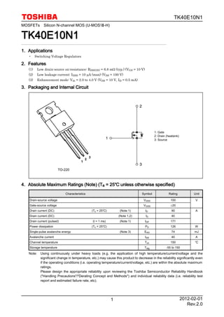
1. TK40E10N1
1
MOSFETs Silicon N-channel MOS (U-MOS-H)
TK40E10N1TK40E10N1TK40E10N1TK40E10N1
1.1.1.1. ApplicationsApplicationsApplicationsApplications
• Switching Voltage Regulators
2.2.2.2. FeaturesFeaturesFeaturesFeatures
(1) Low drain-source on-resistance: RDS(ON) = 6.8 mΩ (typ.) (VGS = 10 V)
(2) Low leakage current: IDSS = 10 µA (max) (VDS = 100 V)
(3) Enhancement mode: Vth = 2.0 to 4.0 V (VDS = 10 V, ID = 0.5 mA)
3.3.3.3. Packaging and Internal CircuitPackaging and Internal CircuitPackaging and Internal CircuitPackaging and Internal Circuit
1: Gate
2: Drain (heatsink)
3: Source
TO-220
4.4.4.4. Absolute Maximum Ratings (Note) (TAbsolute Maximum Ratings (Note) (TAbsolute Maximum Ratings (Note) (TAbsolute Maximum Ratings (Note) (Taaaa = 25= 25= 25= 25 unless otherwise specified)unless otherwise specified)unless otherwise specified)unless otherwise specified)
Characteristics
Drain-source voltage
Gate-source voltage
Drain current (DC)
Drain current (DC)
Drain current (pulsed)
Power dissipation
Single-pulse avalanche energy
Avalanche current
Channel temperature
Storage temperature
(Tc = 25)
(t = 1 ms)
(Tc = 25)
(Note 1)
(Note 1,2)
(Note 1)
(Note 3)
Symbol
VDSS
VGSS
ID
ID
IDP
PD
EAS
IAR
Tch
Tstg
Rating
100
±20
90
40
171
126
74
40
150
-55 to 150
Unit
V
A
W
mJ
A
Note: Using continuously under heavy loads (e.g. the application of high temperature/current/voltage and the
significant change in temperature, etc.) may cause this product to decrease in the reliability significantly even
if the operating conditions (i.e. operating temperature/current/voltage, etc.) are within the absolute maximum
ratings.
Please design the appropriate reliability upon reviewing the Toshiba Semiconductor Reliability Handbook
("Handling Precautions"/"Derating Concept and Methods") and individual reliability data (i.e. reliability test
report and estimated failure rate, etc).
2012-02-01
Rev.2.0
2. TK40E10N1
2
5.5.5.5. Thermal CharacteristicsThermal CharacteristicsThermal CharacteristicsThermal Characteristics
Characteristics
Channel-to-case thermal resistance
Channel-to-ambient thermal resistance
Symbol
Rth(ch-c)
Rth(ch-a)
Max
0.99
83.3
Unit
/W
Note 1: Ensure that the channel temperature does not exceed 150.
Note 2: Device mounted with heatsink so that Rth(ch-a) becomes 3.57/W.
Note 3: VDD = 80 V, Tch = 25 (initial), L = 35.9 µH, RG = 1.2 Ω, IAR = 40 A
Note: This transistor is sensitive to electrostatic discharge and should be handled with care.
2012-02-01
Rev.2.0
3. TK40E10N1
3
6.6.6.6. Electrical CharacteristicsElectrical CharacteristicsElectrical CharacteristicsElectrical Characteristics
6.1.6.1.6.1.6.1. Static Characteristics (TStatic Characteristics (TStatic Characteristics (TStatic Characteristics (Taaaa = 25= 25= 25= 25 unless otherwise specified)unless otherwise specified)unless otherwise specified)unless otherwise specified)
Characteristics
Gate leakage current
Drain cut-off current
Drain-source breakdown voltage
Gate threshold voltage
Drain-source on-resistance
(Note 4)
Symbol
IGSS
IDSS
V(BR)DSS
V(BR)DSX
Vth
RDS(ON)
Test Condition
VGS = ±20 V, VDS = 0 V
VDS = 100 V, VGS = 0 V
ID = 10 mA, VGS = 0 V
ID = 10 mA, VGS = -20 V
VDS = 10 V, ID = 0.5 mA
VGS = 10 V, ID = 20 A
Min
100
65
2.0
Typ.
6.8
Max
±0.1
10
4.0
8.2
Unit
µA
V
mΩ
Note 4: If a reverse bias is applied between gate and source, this device enters V(BR)DSX mode. Note that the drain-
source breakdown voltage is lowered in this mode.
6.2.6.2.6.2.6.2. Dynamic Characteristics (TDynamic Characteristics (TDynamic Characteristics (TDynamic Characteristics (Taaaa = 25= 25= 25= 25 unless otherwise specified)unless otherwise specified)unless otherwise specified)unless otherwise specified)
Characteristics
Input capacitance
Reverse transfer capacitance
Output capacitance
Gate resistance
Switching time (rise time)
Switching time (turn-on time)
Switching time (fall time)
Switching time (turn-off time)
Symbol
Ciss
Crss
Coss
rg
tr
ton
tf
toff
Test Condition
VDS = 50 V, VGS = 0 V, f = 1 MHz
See Figure 6.2.1
Min
Typ.
3000
29
520
2.8
14
35
21
57
Max
Unit
pF
Ω
ns
Fig.Fig.Fig.Fig. 6.2.16.2.16.2.16.2.1 Switching Time Test CircuitSwitching Time Test CircuitSwitching Time Test CircuitSwitching Time Test Circuit
6.3.6.3.6.3.6.3. Gate Charge Characteristics (TGate Charge Characteristics (TGate Charge Characteristics (TGate Charge Characteristics (Taaaa = 25= 25= 25= 25 unless otherwise specified)unless otherwise specified)unless otherwise specified)unless otherwise specified)
Characteristics
Total gate charge (gate-source plus
gate-drain)
Gate-source charge 1
Gate-drain charge
Gate switch charge
Symbol
Qg
Qgs1
Qgd
QSW
Test Condition
VDD ≈ 80 V, VGS = 10 V, ID = 40 A
Min
Typ.
49
18
14
21
Max
Unit
nC
2012-02-01
Rev.2.0
4. TK40E10N1
4
6.4.6.4.6.4.6.4. Source-Drain Characteristics (TSource-Drain Characteristics (TSource-Drain Characteristics (TSource-Drain Characteristics (Taaaa = 25= 25= 25= 25 unless otherwise specified)unless otherwise specified)unless otherwise specified)unless otherwise specified)
Characteristics
Reverse drain current (DC)
Reverse drain current (pulsed)
Diode forward voltage
Reverse recovery time
Reverse recovery charge
(Note 5)
(Note 5)
(Note 6)
(Note 6)
Symbol
IDR
IDRP
VDSF
trr
Qrr
Test Condition
IDR = 40 A, VGS = 0 V
-dIDR/dt = 100 A/µs
Min
Typ.
67
130
Max
40
171
-1.2
Unit
A
V
ns
nC
Note 5: Ensure that the channel temperature does not exceed 150.
Note 6: Ensure that VDS peak does not exceed VDSS.
7.7.7.7. MarkingMarkingMarkingMarking
Fig.Fig.Fig.Fig. 7.17.17.17.1 MarkingMarkingMarkingMarking
2012-02-01
Rev.2.0
9. TK40E10N1
9
RESTRICTIONS ON PRODUCT USERESTRICTIONS ON PRODUCT USERESTRICTIONS ON PRODUCT USERESTRICTIONS ON PRODUCT USE
• Toshiba Corporation, and its subsidiaries and affiliates (collectively "TOSHIBA"), reserve the right to make changes to the information
in this document, and related hardware, software and systems (collectively "Product") without notice.
• This document and any information herein may not be reproduced without prior written permission from TOSHIBA. Even with TOSHIBA's
written permission, reproduction is permissible only if reproduction is without alteration/omission.
• Though TOSHIBA works continually to improve Product's quality and reliability, Product can malfunction or fail. Customers are responsible
for complying with safety standards and for providing adequate designs and safeguards for their hardware, software and systems which
minimize risk and avoid situations in which a malfunction or failure of Product could cause loss of human life, bodily injury or damage
to property, including data loss or corruption. Before customers use the Product, create designs including the Product, or incorporate
the Product into their own applications, customers must also refer to and comply with (a) the latest versions of all relevant TOSHIBA
information, including without limitation, this document, the specifications, the data sheets and application notes for Product and the
precautions and conditions set forth in the "TOSHIBA Semiconductor Reliability Handbook" and (b) the instructions for the application
with which the Product will be used with or for. Customers are solely responsible for all aspects of their own product design or applications,
including but not limited to (a) determining the appropriateness of the use of this Product in such design or applications; (b) evaluating
and determining the applicability of any information contained in this document, or in charts, diagrams, programs, algorithms, sample
application circuits, or any other referenced documents; and (c) validating all operating parameters for such designs and applications.
TOSHIBA ASSUMES NO LIABILITY FOR CUSTOMERS' PRODUCT DESIGN OR APPLICATIONS.TOSHIBA ASSUMES NO LIABILITY FOR CUSTOMERS' PRODUCT DESIGN OR APPLICATIONS.TOSHIBA ASSUMES NO LIABILITY FOR CUSTOMERS' PRODUCT DESIGN OR APPLICATIONS.TOSHIBA ASSUMES NO LIABILITY FOR CUSTOMERS' PRODUCT DESIGN OR APPLICATIONS.
• Product is intended for use in general electronics applications (e.g., computers, personal equipment, office equipment, measuring
equipment, industrial robots and home electronics appliances) or for specific applications as expressly stated in this document. Product
is neither intended nor warranted for use in equipment or systems that require extraordinarily high levels of quality and/or reliability and/
or a malfunction or failure of which may cause loss of human life, bodily injury, serious property damage or serious public impact
("Unintended Use"). Unintended Use includes, without limitation, equipment used in nuclear facilities, equipment used in the aerospace
industry, medical equipment, equipment used for automobiles, trains, ships and other transportation, traffic signaling equipment,
equipment used to control combustions or explosions, safety devices, elevators and escalators, devices related to electric power, and
equipment used in finance-related fields. Do not use Product for Unintended Use unless specifically permitted in this document.
• Do not disassemble, analyze, reverse-engineer, alter, modify, translate or copy Product, whether in whole or in part.
• Product shall not be used for or incorporated into any products or systems whose manufacture, use, or sale is prohibited under any
applicable laws or regulations.
• The information contained herein is presented only as guidance for Product use. No responsibility is assumed by TOSHIBA for any
infringement of patents or any other intellectual property rights of third parties that may result from the use of Product. No license to any
intellectual property right is granted by this document, whether express or implied, by estoppel or otherwise.
• ABSENT A WRITTEN SIGNED AGREEMENT, EXCEPT AS PROVIDED IN THE RELEVANT TERMS AND CONDITIONS OF SALEABSENT A WRITTEN SIGNED AGREEMENT, EXCEPT AS PROVIDED IN THE RELEVANT TERMS AND CONDITIONS OF SALEABSENT A WRITTEN SIGNED AGREEMENT, EXCEPT AS PROVIDED IN THE RELEVANT TERMS AND CONDITIONS OF SALEABSENT A WRITTEN SIGNED AGREEMENT, EXCEPT AS PROVIDED IN THE RELEVANT TERMS AND CONDITIONS OF SALE
FOR PRODUCT, AND TO THE MAXIMUM EXTENT ALLOWABLE BY LAW, TOSHIBA (1) ASSUMES NO LIABILITY WHATSOEVER,FOR PRODUCT, AND TO THE MAXIMUM EXTENT ALLOWABLE BY LAW, TOSHIBA (1) ASSUMES NO LIABILITY WHATSOEVER,FOR PRODUCT, AND TO THE MAXIMUM EXTENT ALLOWABLE BY LAW, TOSHIBA (1) ASSUMES NO LIABILITY WHATSOEVER,FOR PRODUCT, AND TO THE MAXIMUM EXTENT ALLOWABLE BY LAW, TOSHIBA (1) ASSUMES NO LIABILITY WHATSOEVER,
INCLUDING WITHOUT LIMITATION, INDIRECT, CONSEQUENTIAL, SPECIAL, OR INCIDENTAL DAMAGES OR LOSS, INCLUDINGINCLUDING WITHOUT LIMITATION, INDIRECT, CONSEQUENTIAL, SPECIAL, OR INCIDENTAL DAMAGES OR LOSS, INCLUDINGINCLUDING WITHOUT LIMITATION, INDIRECT, CONSEQUENTIAL, SPECIAL, OR INCIDENTAL DAMAGES OR LOSS, INCLUDINGINCLUDING WITHOUT LIMITATION, INDIRECT, CONSEQUENTIAL, SPECIAL, OR INCIDENTAL DAMAGES OR LOSS, INCLUDING
WITHOUT LIMITATION, LOSS OF PROFITS, LOSS OF OPPORTUNITIES, BUSINESS INTERRUPTION AND LOSS OF DATA, ANDWITHOUT LIMITATION, LOSS OF PROFITS, LOSS OF OPPORTUNITIES, BUSINESS INTERRUPTION AND LOSS OF DATA, ANDWITHOUT LIMITATION, LOSS OF PROFITS, LOSS OF OPPORTUNITIES, BUSINESS INTERRUPTION AND LOSS OF DATA, ANDWITHOUT LIMITATION, LOSS OF PROFITS, LOSS OF OPPORTUNITIES, BUSINESS INTERRUPTION AND LOSS OF DATA, AND
(2) DISCLAIMS ANY AND ALL EXPRESS OR IMPLIED WARRANTIES AND CONDITIONS RELATED TO SALE, USE OF PRODUCT,(2) DISCLAIMS ANY AND ALL EXPRESS OR IMPLIED WARRANTIES AND CONDITIONS RELATED TO SALE, USE OF PRODUCT,(2) DISCLAIMS ANY AND ALL EXPRESS OR IMPLIED WARRANTIES AND CONDITIONS RELATED TO SALE, USE OF PRODUCT,(2) DISCLAIMS ANY AND ALL EXPRESS OR IMPLIED WARRANTIES AND CONDITIONS RELATED TO SALE, USE OF PRODUCT,
OR INFORMATION, INCLUDING WARRANTIES OR CONDITIONS OF MERCHANTABILITY, FITNESS FOR A PARTICULAROR INFORMATION, INCLUDING WARRANTIES OR CONDITIONS OF MERCHANTABILITY, FITNESS FOR A PARTICULAROR INFORMATION, INCLUDING WARRANTIES OR CONDITIONS OF MERCHANTABILITY, FITNESS FOR A PARTICULAROR INFORMATION, INCLUDING WARRANTIES OR CONDITIONS OF MERCHANTABILITY, FITNESS FOR A PARTICULAR
PURPOSE, ACCURACY OF INFORMATION, OR NONINFRINGEMENT.PURPOSE, ACCURACY OF INFORMATION, OR NONINFRINGEMENT.PURPOSE, ACCURACY OF INFORMATION, OR NONINFRINGEMENT.PURPOSE, ACCURACY OF INFORMATION, OR NONINFRINGEMENT.
• Do not use or otherwise make available Product or related software or technology for any military purposes, including without limitation,
for the design, development, use, stockpiling or manufacturing of nuclear, chemical, or biological weapons or missile technology products
(mass destruction weapons). Product and related software and technology may be controlled under the Japanese Foreign Exchange
and Foreign Trade Law and the U.S. Export Administration Regulations. Export and re-export of Product or related software or technology
are strictly prohibited except in compliance with all applicable export laws and regulations.
• Please contact your TOSHIBA sales representative for details as to environmental matters such as the RoHS compatibility of Product.
Please use Product in compliance with all applicable laws and regulations that regulate the inclusion or use of controlled substances,
including without limitation, the EU RoHS Directive. TOSHIBA assumes no liability for damages or losses occurring as a result of
noncompliance with applicable laws and regulations.
2012-02-01
Rev.2.0