Tps3306 18 (1)
•
0 likes•65 views

The TPS3306 family is a series of dual supervisory circuits that monitor two independent supply voltages for DSP and processor-based systems. They monitor supply voltages like 3.3V/1.5V, 3.3V/1.8V, or 3.3V/2.5V. The circuits assert a reset signal when supply voltages drop below threshold levels and include a watchdog timer and power-fail comparator. They are available in 8-pin packages and operate over a temperature range of -40°C to 85°C.

More Related Content
What's hot
What's hot (20)
Viewers also liked
Similar to Tps3306 18 (1)
Similar to Tps3306 18 (1) (20)
More from ____
Recently uploaded
Recently uploaded (20)
Tps3306 18 (1)
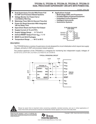
- 1. TPS3306-15, TPS3306-18, TPS3306-20, TPS3306-25, TPS3306-33 DUAL PROCESSOR SUPERVISORY CIRCUITS WITH POWER-FAIL SLVS290 – APRIL 2000 1POST OFFICE BOX 655303 • DALLAS, TEXAS 75265 D Dual Supervisory Circuits With Power-Fail for DSP and Processor-Based Systems D Voltage Monitor for Power-Fail or Low-Battery Warning D Watchdog Timer With 0.8 Second Time-Out D Power-On Reset Generator With Integrated 100 ms Delay Time D Open-Drain Reset and Power-Fail Output D Supply Current of 15 µA (TYP.) D Supply Voltage Range . . . 2.7 V to 6 V D Defined RESET Output From VDD ≥ 1.1 V D MSOP-8 and SO-8 Packages D Temperature Range . . . – 40°C to 85°C D Applications Include – Multivoltage DSPs and Processors – Portable Battery-Powered Equipment – Embedded Control Systems – Intelligent Instruments – Automotive Systems description The TPS3306 family is a series of supervisory circuits designed for circuit initialization which require two supply voltages, primarily in DSP and processor-based systems. The product spectrum of the TPS3306-xx is designed for monitoring two independent supply voltages of 3.3 V/1.5 V, 3.3 V/1.8 V, 3.3 V/2 V, 3.3 V/2.5 V, or 3.3 V/5 V. TYPICAL OPERATING CIRCUIT SENSE1 SENSE2 PFI GND VDD WDI PFO RESET TPS3306–15 R3 R4 R1 1% R2 1% AVDD CVDD DVDD B_XF A_XF RESET VSS VSSA TMS320 VC5441 3.3 V 1.5 V PRODUCTION DATA information is current as of publication date. Products conform to specifications per the terms of Texas Instruments standard warranty. Production processing does not necessarily include testing of all parameters. Copyright © 2000, Texas Instruments Incorporated Please be aware that an important notice concerning availability, standard warranty, and use in critical applications of Texas Instruments semiconductor products and disclaimers thereto appears at the end of this data sheet. 1 2 3 4 8 7 6 5 SENSE1 SENSE2 PFI GND VDD WDI PFO RESET D OR DGK PACKAGE (TOP VIEW)
- 2. TPS3306-15, TPS3306-18, TPS3306-20, TPS3306-25, TPS3306-33 DUAL PROCESSOR SUPERVISORY CIRCUITS WITH POWER-FAIL SLVS290 – APRIL 2000 2 POST OFFICE BOX 655303 • DALLAS, TEXAS 75265 description (continued) The various supervisory circuits are designed to monitor the nominal supply voltage, as shown in the following supply voltage monitoring table. SUPPLY VOLTAGE MONITORING DEVICE NOMINAL SUPERVISED VOLTAGE THRESHOLD VOLTAGE (TYP) DEVICE SENSE1 SENSE2 SENSE1 SENSE2 TPS3306-15 3.3 V 1.5 V 2.93 V 1.4 V TPS3306-18 3.3 V 1.8 V 2.93 V 1.68 V TPS3306-20 3.3 V 2 V 2.93 V 1.85 V TPS3306-25 3.3 V 2.5 V 2.93 V 2.25 V TPS3306-33 5 V 3.3 V 4.55 V 2.93 V During power-on, RESET is asserted when the supply voltage VDD becomes higher than 1.1 V. Thereafter, the supervisory circuits monitor the SENSEn inputs and keep RESET active as long as SENSEn remains below the threshold voltage VIT. An internal timer delays the return of the RESET output to the inactive state (high) to ensure proper system reset. The delay time, td(typ) = 100 ms, starts after SENSE1 and SENSE2 inputs have risen above the threshold voltage VIT. When the voltage at SENSE1 or SENSE2 input drops below the threshold voltage VIT, the output becomes active (low) again. The integrated power-fail (PFI) comparator with separate open-drain (PFO) output can be used for low-battery detection, power-fail warning, or for monitoring a power supply other than the main supply. The TPS3306-xx devices integrate a watchdog timer that is periodically triggered by a positive or negative transition of WDI. When the supervising system fails to retrigger the watchdog circuit within the time-out interval, tt(out) = 0.50 s, RESET becomes active for the time period td . This event also reinitializes the watchdog timer. Leaving WDI unconnected disables the watchdog. The TPS3306-xx devices are available in either 8-pin MSOP or standard 8-pin SO packages. The TPS3306-xx family is characterized for operation over a temperature range of – 40°C to 85°C. AVAILABLE OPTIONS PACKAGED DEVICES MARKING TA SMALL OUTLINE (D) µ-SMALL OUTLINE (DGK) MARKING DGK PACKAGE TPS3305-15D TPS3306-15DGK TIAIC TPS3305-18D TPS3306-18DGK TIAID –40_C to 85_C TPS3305-20D TPS3306-20DGK TIAIE TPS3305-25D TPS3306-25DGK TIAIF TPS3305-33D TPS3306-33DGK TIAIG
- 3. TPS3306-15, TPS3306-18, TPS3306-20, TPS3306-25, TPS3306-33 DUAL PROCESSOR SUPERVISORY CIRCUITS WITH POWER-FAIL SLVS290 – APRIL 2000 3POST OFFICE BOX 655303 • DALLAS, TEXAS 75265 description (continued) FUNCTION/TRUTH TABLES SENSE1>VIT1 SENSE2>VIT2 RESET 0 0 L 0 1 L 1 0 L 1 1 H FUNCTION/TRUTH TABLES PFI>VIT PFO TYPICAL DELAY 0→1 L→H 0.5 µs 1→0 H→L 0.5 µs functional block diagram _ + _ + R4 R3 Reference Voltage of 1.25 V RESET Logic + Timer Oscillator SENSE 1 SENSE 2 GND WDI PFO RESET TPS3306 Watchdog Logic + Timer 40 kΩ Transition Detection R2 R1 _ +PFI VDD
- 4. TPS3306-15, TPS3306-18, TPS3306-20, TPS3306-25, TPS3306-33 DUAL PROCESSOR SUPERVISORY CIRCUITS WITH POWER-FAIL SLVS290 – APRIL 2000 4 POST OFFICE BOX 655303 • DALLAS, TEXAS 75265 timing diagram t t t tdtd td RESET Because of Power-Down RESET Because of WDI RESET Because of a Power Drop Below VIT– RESET Because of Power-Up tt(out) SENSEn V(nom) VIT 1.1 V WDI 1 0 RESET 1 0 Undefined Behavior Undefined Behavior Terminal Functions TERMINAL I/O DESCRIPTION NAME NO. I/O DESCRIPTION GND 4 I Ground PFI 3 I Power-fail comparator input PFO 6 O Power-fail comparator output, open-drain RESET 5 O Active-low reset output, open-drain SENSE1 1 I Sense voltage input 1 SENSE2 2 I Sense voltage input 2 WDI 7 I Watchdog timer input VDD 8 I Supply voltage detailed description watchdog In a microprocessor- or DSP-based system, it is not only important to supervise the supply voltage, it is also important to ensure correct program execution. The task of a watchdog is to ensure that the program is not stalled in an indefinite loop. The microprocessor, microcontroller, or DSP has to typically toggle the watchdog input within 0.8 s to avoid a time out occurring. Either a low-to-high or a high-to-low transition resets the internal watchdog timer. If the input is unconnected or tied with a high impedance driver, the watchdog is disabled and will be retriggered internally.
- 5. TPS3306-15, TPS3306-18, TPS3306-20, TPS3306-25, TPS3306-33 DUAL PROCESSOR SUPERVISORY CIRCUITS WITH POWER-FAIL SLVS290 – APRIL 2000 5POST OFFICE BOX 655303 • DALLAS, TEXAS 75265 detailed description (continued) saving current while using the watchdog The watchdog input is internally driven low during the first 7/8 of the watchdog time-out period, then momentarily pulses high, resetting the watchdog counter. For minimum watchdog input current (minimum overall power consump- tion), leave WDI low for the majority of the watchdog time-out period, pulsing it low-high-low once within 7/8 of the watchdog time-out period to reset the watchdog timer. If instead WDI is externally driven high for the majority of the time-out period, a current of 5 V/40 kΩ ≈ 125 µA can flow into WDI. td td t(tout) VDD VIT WDI RESET t t t Figure 1. Watchdog Timing power-fail comparator (PFI & PFO) An additional comparator is provided to monitor voltages other than the nominal supply voltage. The power-fail-input (PFI) will be compared with an internal voltage reference of 1.25 V. If the input voltage falls below the power-fail thresh- old (VPFI) of typ. 1.25 V, the power-fail output (PFO) goes low. If it goes above 1.25 V plus about 10 mV hysteresis, the output returns to high. By connecting 2 external resistors, it is possible to supervise any voltages above 1.25 V. The sum of both resistors should be about 1 MΩ, to minimize power consumption and also to assure that the current in the PFI pin can be neglected compared with the current through the resistor network. The tolerance of the external resis- tors should be not more than 1% to ensure minimal variation of sensed voltage. If the power-fail comparator is unused, connect PFI to ground and leave PFO unconnected. PFI PFO VCC GND TPS3306 V(SENSE) R1 1% R2 1% VPFI,trip = 1.25 V × R1 + R2 R2
- 6. TPS3306-15, TPS3306-18, TPS3306-20, TPS3306-25, TPS3306-33 DUAL PROCESSOR SUPERVISORY CIRCUITS WITH POWER-FAIL SLVS290 – APRIL 2000 6 POST OFFICE BOX 655303 • DALLAS, TEXAS 75265 absolute maximum ratings over operating free-air temperature range (unless otherwise noted)† Supply voltage, VDD (see Note1) 7 V. . . . . . . . . . . . . . . . . . . . . . . . . . . . . . . . . . . . . . . . . . . . . . . . . . . . . . . . . . . . . All other pins (see Note 1) – 0.3 V to 7 V. . . . . . . . . . . . . . . . . . . . . . . . . . . . . . . . . . . . . . . . . . . . . . . . . . . . . . . . . . Maximum low output current, IOL 5 mA. . . . . . . . . . . . . . . . . . . . . . . . . . . . . . . . . . . . . . . . . . . . . . . . . . . . . . . . . . . Maximum high output current, IOH – 5 mA. . . . . . . . . . . . . . . . . . . . . . . . . . . . . . . . . . . . . . . . . . . . . . . . . . . . . . . . . Input clamp current, IIK (VI < 0 or VI > VDD) ±20 mA. . . . . . . . . . . . . . . . . . . . . . . . . . . . . . . . . . . . . . . . . . . . . . . . Output clamp current, IOK (VO < 0 or VO > VDD) ±20 mA. . . . . . . . . . . . . . . . . . . . . . . . . . . . . . . . . . . . . . . . . . . . Continuous total power dissipation See Dissipation Rating Table. . . . . . . . . . . . . . . . . . . . . . . . . . . . . . . . . . . . . Operating free-air temperature range, TA –40°C to 85°C. . . . . . . . . . . . . . . . . . . . . . . . . . . . . . . . . . . . . . . . . . . Storage temperature range, Tstg –65°C to 150°C. . . . . . . . . . . . . . . . . . . . . . . . . . . . . . . . . . . . . . . . . . . . . . . . . . . Soldering temperature 260_C. . . . . . . . . . . . . . . . . . . . . . . . . . . . . . . . . . . . . . . . . . . . . . . . . . . . . . . . . . . . . . . . . . . . † Stresses beyond those listed under “absolute maximum ratings” may cause permanent damage to the device. These are stress ratings only, and functional operation of the device at these or any other conditions beyond those indicated under “recommended operating conditions” is not implied. Exposure to absolute-maximum-rated conditions for extended periods may affect device reliability. NOTE 1: All voltage values are with respect to GND. For reliable operation, the device must not be operated at 7 V for more than t = 1000 h continuously. DISSIPATION RATING TABLE PACKAGE TA ≤ 25°C POWER RATING DERATING FACTOR ABOVE TA = 25°C TA = 70°C POWER RATING TA = 85°C POWER RATING DGK 424 mW 3.4 mW/°C 271 mW 220 mW D 725 mW 5.8 mW/°C 464 mW 377 mW recommended operating conditions at specified temperature range MIN MAX UNIT Supply voltage, VDD 2.7 6 V Input voltage at WDI and PFI, VI 0 VDD+0.3 V Input voltage at SENSE1 and SENSE2, VI 0 (VDD+0.3)VIT/1.25 V V High-level input voltage at WDI, VIH 0.7xVDD V Low-level input voltage at WDI, VIL 0.3×VDD V Operating free-air temperature range, TA –40 85 °C
- 7. TPS3306-15, TPS3306-18, TPS3306-20, TPS3306-25, TPS3306-33 DUAL PROCESSOR SUPERVISORY CIRCUITS WITH POWER-FAIL SLVS290 – APRIL 2000 7POST OFFICE BOX 655303 • DALLAS, TEXAS 75265 electrical characteristics over recommended operating free-air temperature range (unless otherwise noted) PARAMETER TEST CONDITIONS MIN TYP MAX UNIT VDD = 2.7 V to 6 V, IOL = 20 µA 0.2 VOL Low-level output voltage RESET, PFO VDD = 3.3 V, IOL = 2 mA 0.4 V PFO VDD = 6 V, IOL = 3 mA 0.4 Power-up reset voltage (see Note 2) VDD ≥ 1.1 V, IOL = 20 µA 0.4 V 1.37 1.40 1.43 1.64 1.68 1.72 VSENSE1, V 2 7 V to 6 V 1.81 1.85 1.89 VSENSE2 VDD = 2.7 V to 6 V, TA = 0°C to 85°C 2.20 2.25 2.30 V TA = 0°C to 85°C 2.86 2.93 3 4.46 4.55 4.64 VIT Negative-going input threshold voltage PFI 1.22 1.25 1.28 VIT g g g g (see Note 3) 1.37 1.40 1.44 1.64 1.68 1.73 VSENSE1, V 2 7 V to 6 V 1.81 1.85 1.90 VSENSE2 VDD = 2.7 V to 6 V, TA = –40°C to 85°C 2.20 2.25 2.32 V TA = –40°C to 85°C 2.86 2.93 3.02 4.46 4.55 4.67 PFI 1.22 1.25 1.29 PFI VIT = 1.25 V 10 VIT = 1.40 V 15 VIT = 1.68 V 15 Vhys Hysteresis VSENSEn VIT = 1.86 V 20 mVy VSENSEn VIT = 2.25 V 20 VIT = 2.93 V 30 VIT = 4.55 V 40 IH(AV) Average high-level input current WDI WDI = VDD = 6 V Time average (dc = 88%) 100 150 µA IL(AV) Average low-level input current WDI WDI = 0 V, VDD = 6 V, Time average (dc = 12%) –15 –20 µA WDI WDI = VDD = 6 V, 120 170 IH High-level input current SENSE1 VSENSE1 = VDD = 6 V 5 8 µA SENSE2 VSENSE2 = VDD = 6 V 6 9 IL Low-level input current WDI WDI = 0 V, VDD, = 6 V –120 –170 µA II Input current PFI VDD = 6 V, 0 V ≤ VI ≤ VDD –25 25 nA IDD Supply current 15 40 µA Ci Input capacitance VI = 0 V to VDD 10 pF NOTES: 2. The lowest supply voltage at which RESET becomes active. tr, VDD ≥ 15 µs/V. 3. To ensure best stability of the threshold voltage, a bypass capacitor (ceramic 0.1 µF) should be placed close to the supply terminals.
- 8. TPS3306-15, TPS3306-18, TPS3306-20, TPS3306-25, TPS3306-33 DUAL PROCESSOR SUPERVISORY CIRCUITS WITH POWER-FAIL SLVS290 – APRIL 2000 8 POST OFFICE BOX 655303 • DALLAS, TEXAS 75265 timing requirements at VDD = 2.7 V to 6 V, RL = 1 MΩ, CL = 50 pF, TA = 25°C PARAMETER TEST CONDITIONS MIN TYP MAX UNIT t Pulse width SENSEn VSENSEnL = VIT –0.2 V, VSENSEnH = VIT +0.2 V 6 µs tw Pulse width WDI VIH = 0.7 × VDD, VIL = 0.3 × VDD 100 ns switching characteristics at VDD = 2.7 V to 6 V, RL = 1 MΩ, CL = 50 pF, TA = 25°C PARAMETER TEST CONDITIONS MIN TYP MAX UNIT tt(out) Watchdog time out VI(SENSEn) ≥ VIT + 0.2 V, See timing diagram 0.5 0.8 1.2 s td Delay time VI(SENSEn) ≥ VIT + 0.2 V, See timing diagram 70 100 140 ms tPHL Propagation (delay) time, high-to-low level output SENSEn to RESET VIH = VIT +0.2 V, VIL = VIT –0.2 V 1 5 µs tPHL Propagation (delay) time, high-to-low level output PFI to PFO 0 5 1 µs tPLH Propagation (delay) time, low-to-high level output PFI to PFO 0.5 1 µs TYPICAL CHARACTERISTICS Figure 2 1 0.999 0.997 0.995 –40 –15 10 35 NormalizedInputThresholdVoltage–VIT(TA),VIT(25) 1.002 1.003 NORMALIZED SENSE THRESHOLD VOLTAGE vs FREE-AIR TEMPERATURE AT VDD 1.005 60 85 VDD = 6 V 1.004 1.001 0.998 0.996 C° TA – Free-Air Temperature – °C Figure 3 4 0 –6 –10 –0.5 0 0.5 1 2.5 3 3.5 –SupplyCurrent– 8 14 SUPPLY CURRENT vs SUPPLY VOLTAGE 18 4 5 6 7 16 12 10 6 2 –2 –4 –8 1.5 2 4.5 5.5 6.5 IDDAµ VDD – Supply Voltage – V SENSEn = VDD TA = 25°C TPS3306–33
- 9. TPS3306-15, TPS3306-18, TPS3306-20, TPS3306-25, TPS3306-33 DUAL PROCESSOR SUPERVISORY CIRCUITS WITH POWER-FAIL SLVS290 – APRIL 2000 9POST OFFICE BOX 655303 • DALLAS, TEXAS 75265 TYPICAL CHARACTERISTICS Figure 4 0 0.4 0.8 1.2 1.6 2 2.4 2.8 0 1 2 3 4 5 6 7 8 9 10 11 12 13 85°C –40°C VDD = 2.7 V –Low-LevelOutputVoltage–V LOW-LEVEL OUTPUT VOLTAGE vs LOW-LEVEL OUTPUT CURRENT IOL – Low-Level Output Current – mA VOL Figure 5 3.5 3 1.5 0 0 5 10 15 20 30 35 4.5 5.5 6.5 40 50 55 60 85°C –40°C VDD = 6 V –Low-LevelOutputVoltage–V LOW-LEVEL OUTPUT VOLTAGE vs LOW-LEVEL OUTPUT CURRENT IOL – Low-Level Output Current – mA VOL 6 5 4 2.5 2 1 0.5 25 45 Figure 6 5 4 2 0 0 100 200 300 400 500 600 –MinimumPulseDurationat 7 9 MINIMUM PULSE DURATION AT SENSE vs THRESHOLD OVERDRIVE 10 700 800 900 1000 8 6 3 1 SENSE – Threshold Overdrive – mV twVsense–sµ VDD = 6 V
- 10. TPS3306-15, TPS3306-18, TPS3306-20, TPS3306-25, TPS3306-33 DUAL PROCESSOR SUPERVISORY CIRCUITS WITH POWER-FAIL SLVS290 – APRIL 2000 10 POST OFFICE BOX 655303 • DALLAS, TEXAS 75265 MECHANICAL DATA D (R-PDSO-G**) PLASTIC SMALL-OUTLINE PACKAGE 14 PIN SHOWN 4040047/D 10/96 0.228 (5,80) 0.244 (6,20) 0.069 (1,75) MAX 0.010 (0,25) 0.004 (0,10) 1 14 0.014 (0,35) 0.020 (0,51) A 0.157 (4,00) 0.150 (3,81) 7 8 0.044 (1,12) 0.016 (0,40) Seating Plane 0.010 (0,25) PINS ** 0.008 (0,20) NOM A MIN A MAX DIM Gage Plane 0.189 (4,80) (5,00) 0.197 8 (8,55) (8,75) 0.337 14 0.344 (9,80) 16 0.394 (10,00) 0.386 0.004 (0,10) M0.010 (0,25) 0.050 (1,27) 0°–8° NOTES: A. All linear dimensions are in inches (millimeters). B. This drawing is subject to change without notice. C. Body dimensions do not include mold flash or protrusion, not to exceed 0.006 (0,15). D. Falls within JEDEC MS-012
- 11. TPS3306-15, TPS3306-18, TPS3306-20, TPS3306-25, TPS3306-33 DUAL PROCESSOR SUPERVISORY CIRCUITS WITH POWER-FAIL SLVS290 – APRIL 2000 11POST OFFICE BOX 655303 • DALLAS, TEXAS 75265 MECHANICAL DATA DGK (R-PDSO-G8) PLASTIC SMALL-OUTLINE PACKAGE 0,69 0,41 0,25 0,15 NOM Gage Plane 4073329/B 04/98 4,98 0,25 5 3,05 4,782,95 8 4 3,05 2,95 1 0,38 1,07 MAX Seating Plane 0,65 M0,25 0°–6° 0,10 0,15 0,05 NOTES: A. All linear dimensions are in millimeters. B. This drawing is subject to change without notice. C. Body dimensions do not include mold flash or protrusion. D. Falls within JEDEC MO-187
- 12. IMPORTANT NOTICE Texas Instruments and its subsidiaries (TI) reserve the right to make changes to their products or to discontinue any product or service without notice, and advise customers to obtain the latest version of relevant information to verify, before placing orders, that information being relied on is current and complete. All products are sold subject to the terms and conditions of sale supplied at the time of order acknowledgment, including those pertaining to warranty, patent infringement, and limitation of liability. TI warrants performance of its semiconductor products to the specifications applicable at the time of sale in accordance with TI’s standard warranty. Testing and other quality control techniques are utilized to the extent TI deems necessary to support this warranty. Specific testing of all parameters of each device is not necessarily performed, except those mandated by government requirements. Customers are responsible for their applications using TI components. In order to minimize risks associated with the customer’s applications, adequate design and operating safeguards must be provided by the customer to minimize inherent or procedural hazards. TI assumes no liability for applications assistance or customer product design. TI does not warrant or represent that any license, either express or implied, is granted under any patent right, copyright, mask work right, or other intellectual property right of TI covering or relating to any combination, machine, or process in which such semiconductor products or services might be or are used. TI’s publication of information regarding any third party’s products or services does not constitute TI’s approval, warranty or endorsement thereof. Copyright © 2000, Texas Instruments Incorporated
- 13. This datasheet has been download from: www.datasheetcatalog.com Datasheets for electronics components.