Downloaded 81 times
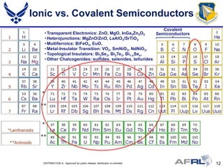

![Transport in ZnO
Dave Look, Wright State
•[VZn ] = 1.7x10²⁰
Pulse Laser cm-3 gives
32 Deposition E(formation) =
in Ar 0.2 eV; provides
accurate check
30
Mobility (cm /V s)
on theory (DFT)
µ (ND, NA, m*, T) •Reduced [VZn ]
2
Fitting parameters: m* with Zn anneals:
28 21 -3 0.30 got = 1.4x10⁻⁴
ND = 1.45 x 10 cm SIMS
20 -3
-cm, 3rd best in
NA = 1.71 x 10 cm Positron 0.34 world
26 m* = 0.34m0 Kane model •Future: create
0.40 GaZn donors by
filling VZn with Ga
24 •Future: apply
0 100 200 300 methods to other
TMOs
T (K)
DISTRIBUTION A: Approved for public release; distribution is unlimited. 15](https://image.slidesharecdn.com/1-hwang-ghz-thzelectronics-120713095140-phpapp02/85/Hwang-GHz-THz-Electronics-Spring-Review-2012-15-320.jpg)

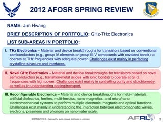
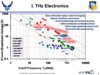
The document outlines advancements and challenges in GHz-THz electronics research, focusing on material and device breakthroughs for transistors using both conventional and novel semiconductors. It highlights key areas such as THz electronics, novel GHz electronics, and reconfigurable electronics, with discussion on various applications and the need for improved crystalline structures, purity control, and understanding of nanometer-scale interactions. The report emphasizes collaboration among various organizations to explore new technologies and improve semiconductor performance.