Download as PDF, PPTX
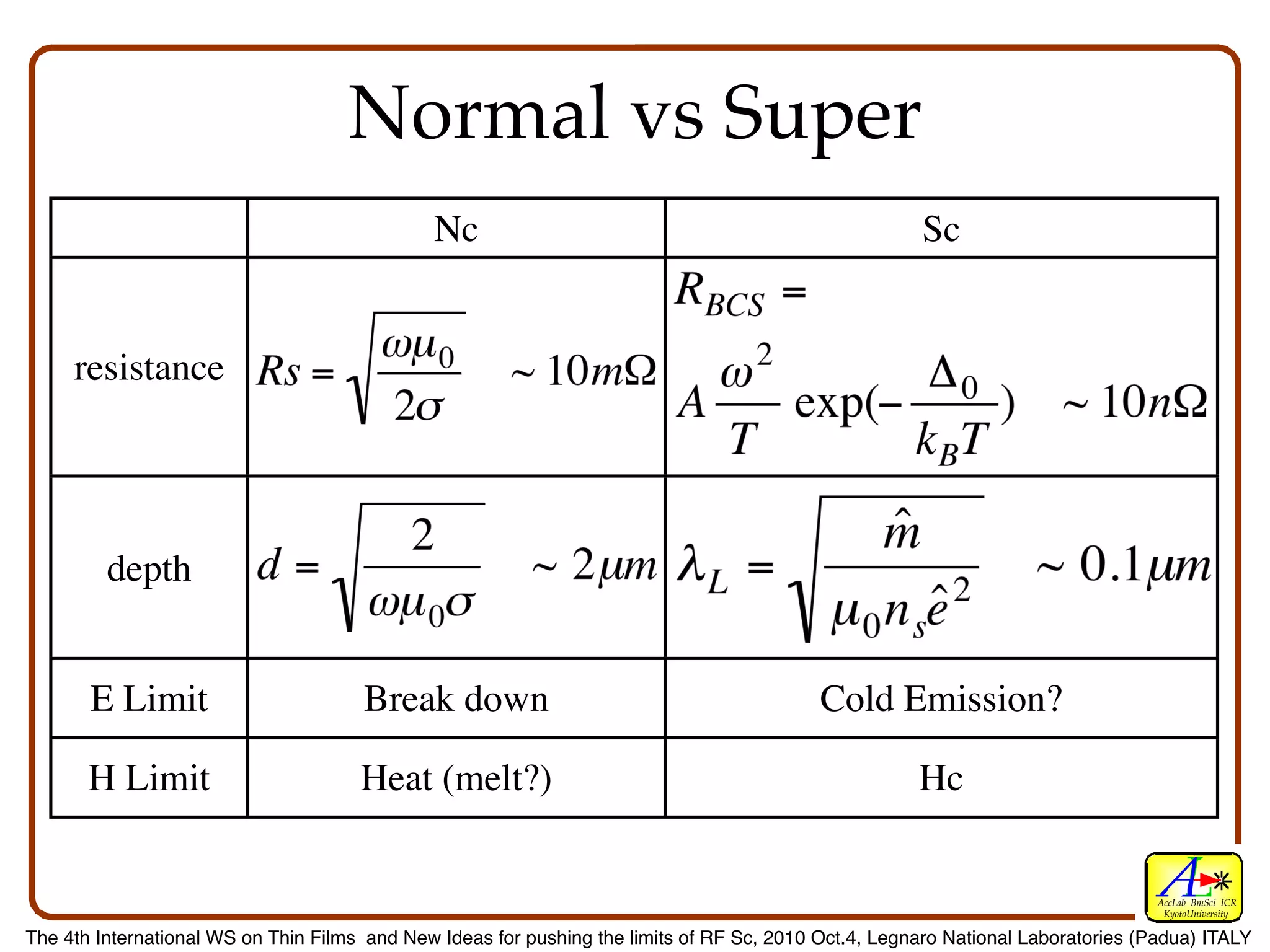
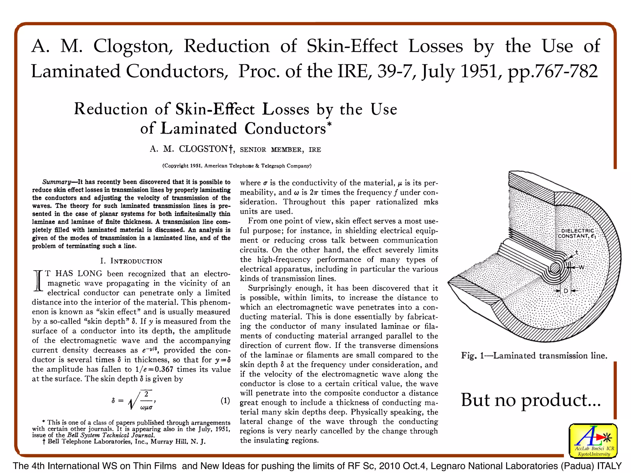
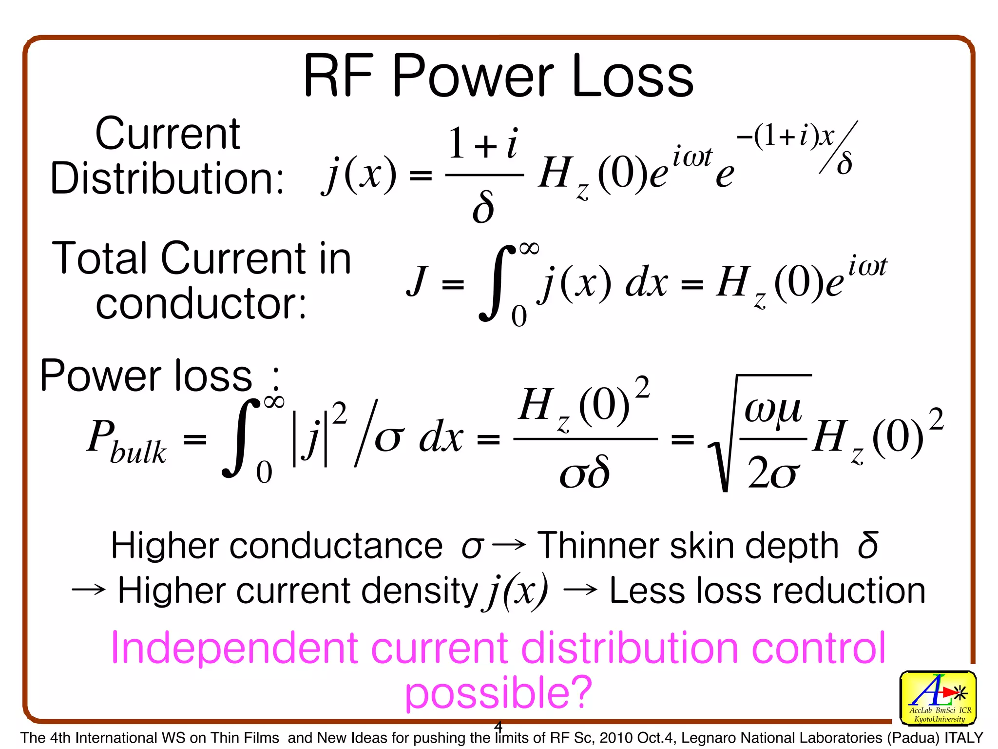
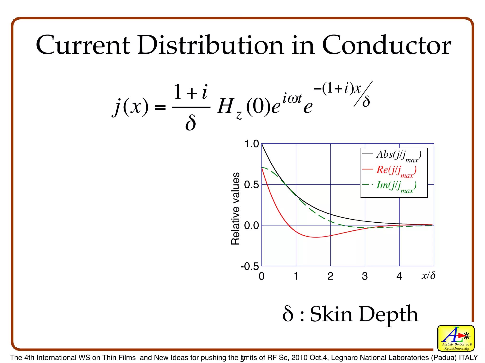
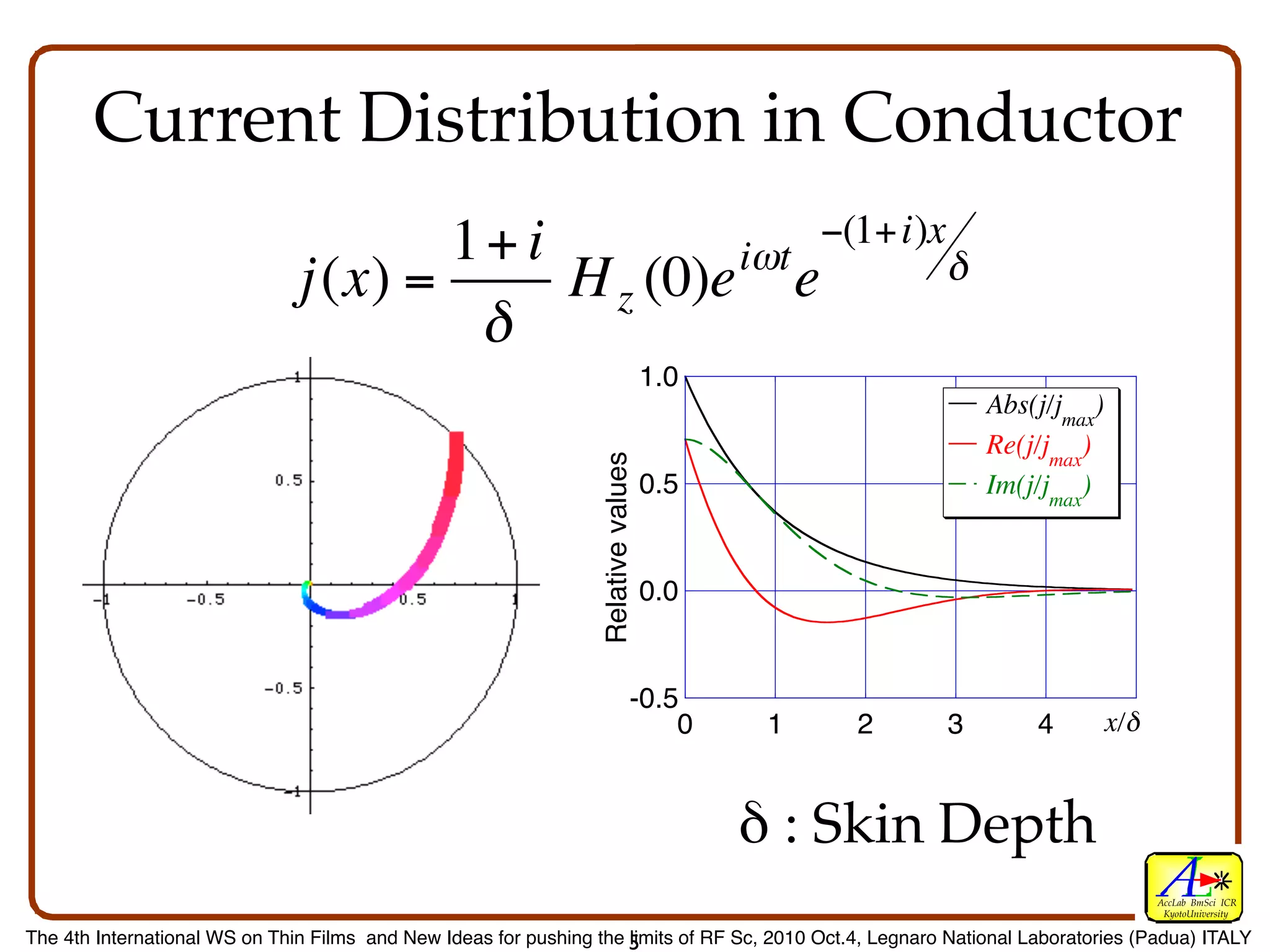
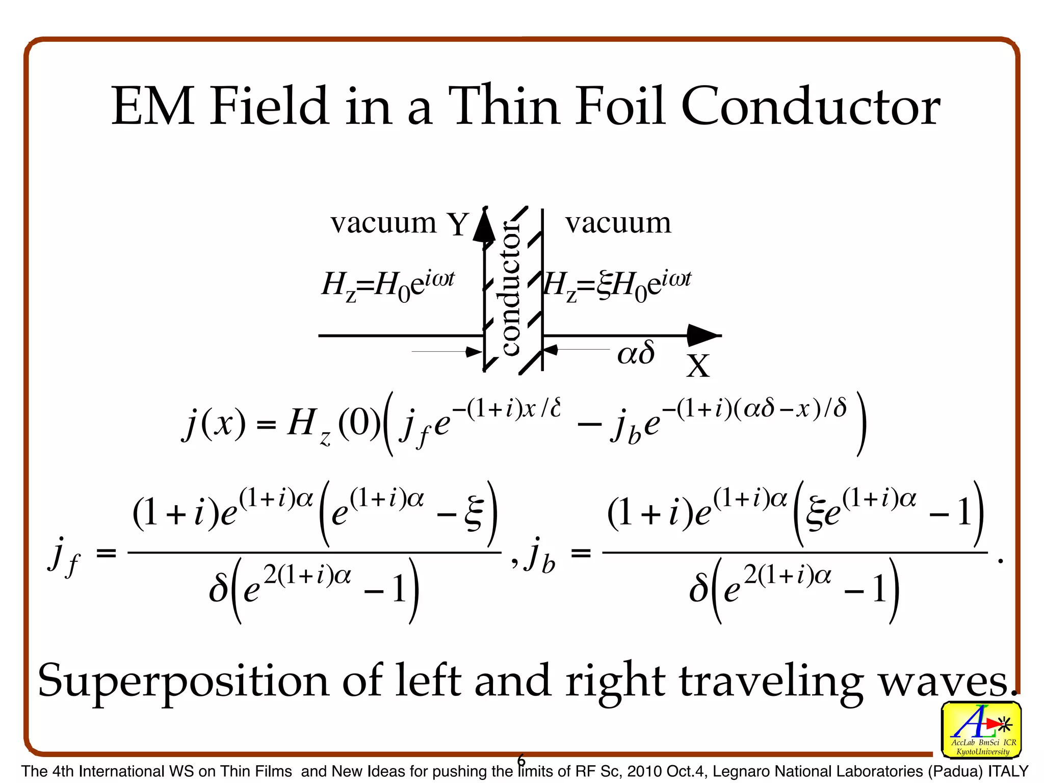
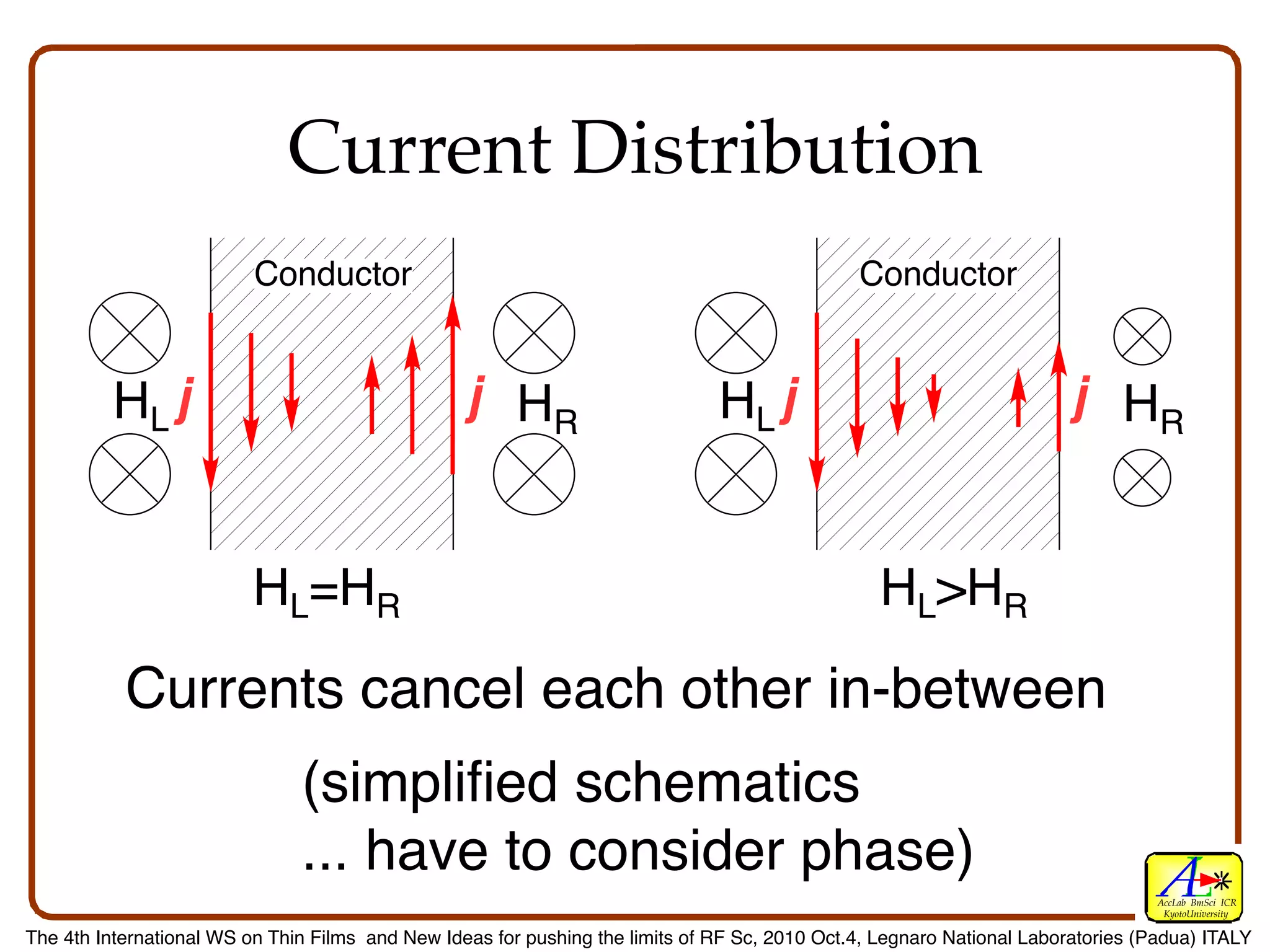
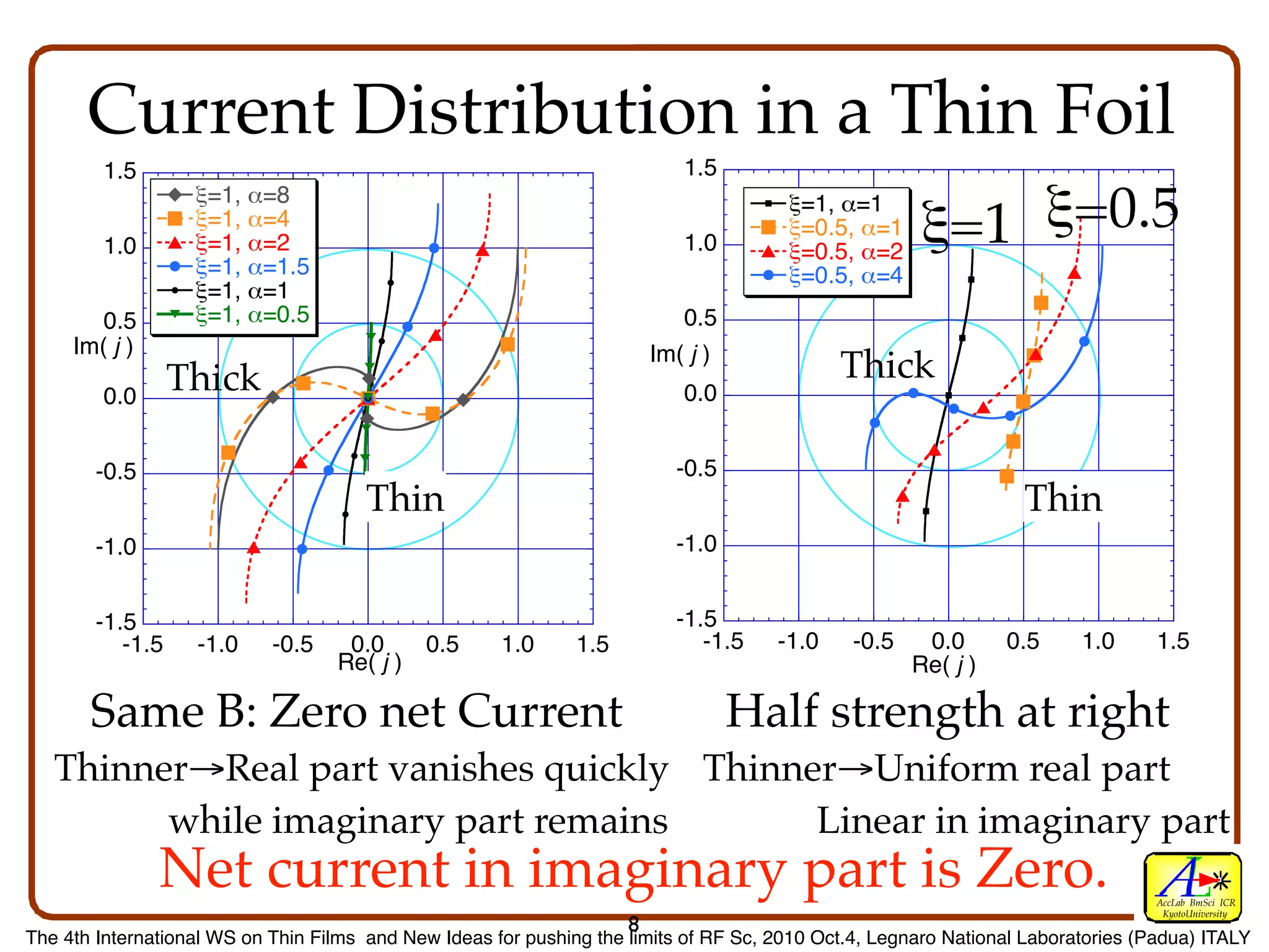
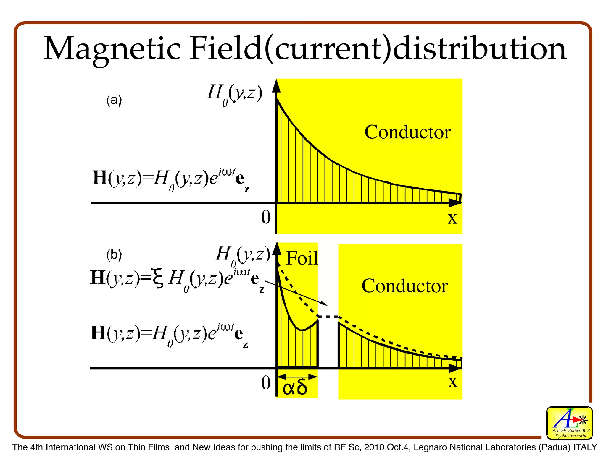
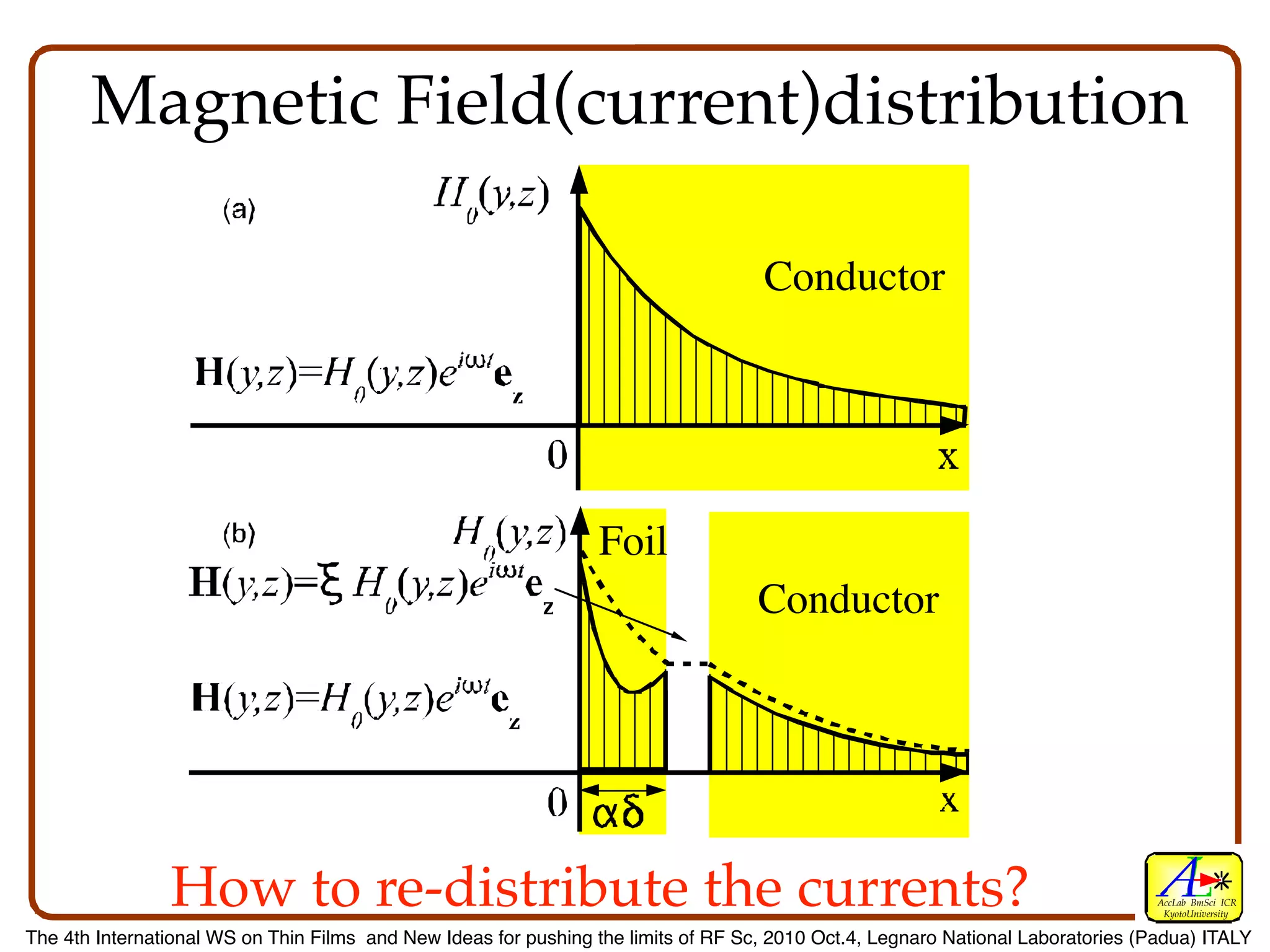
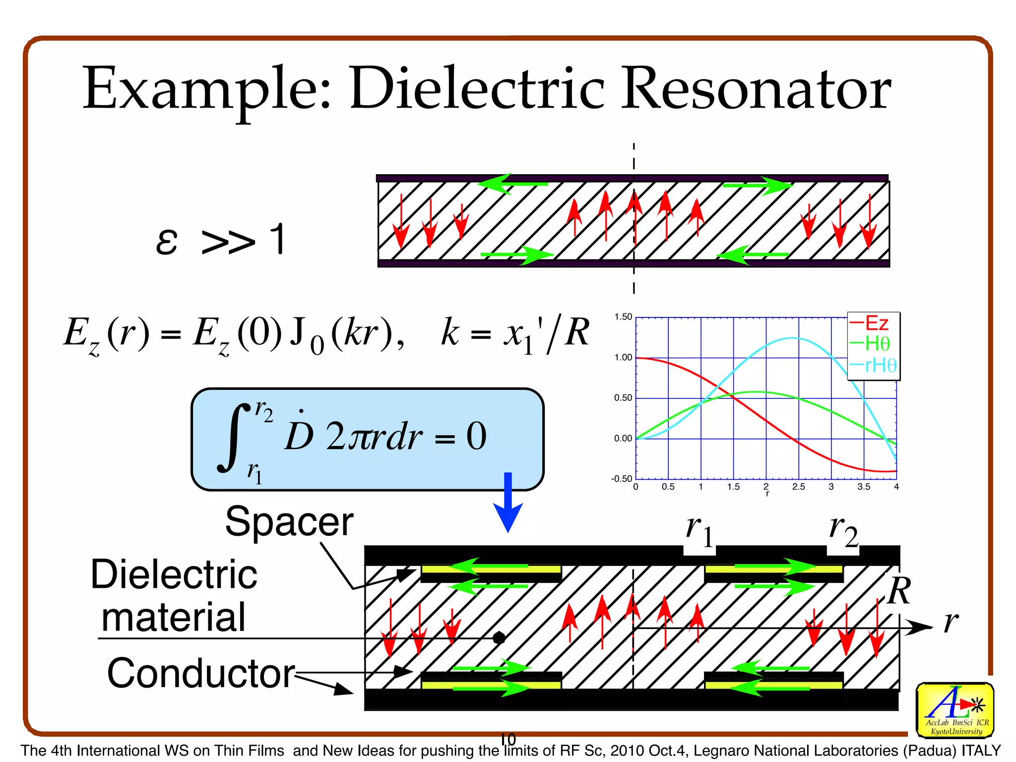
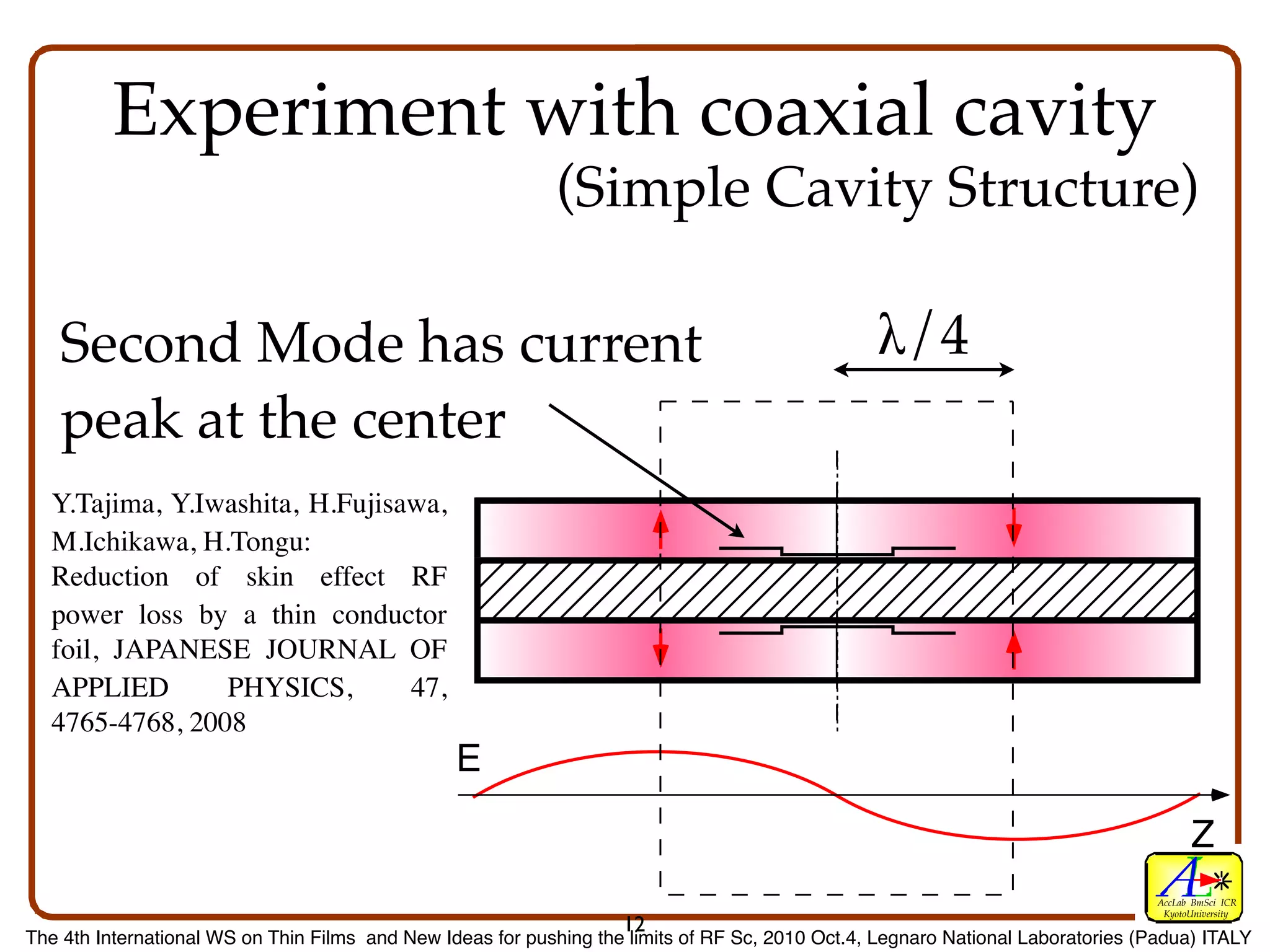
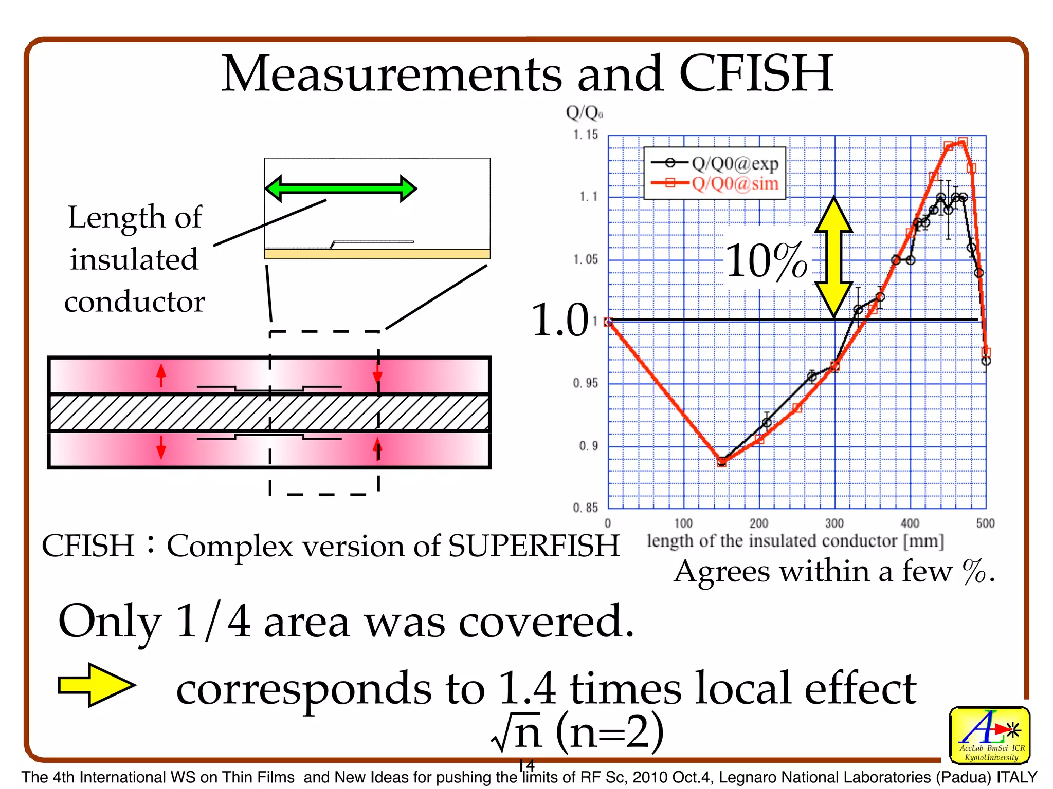
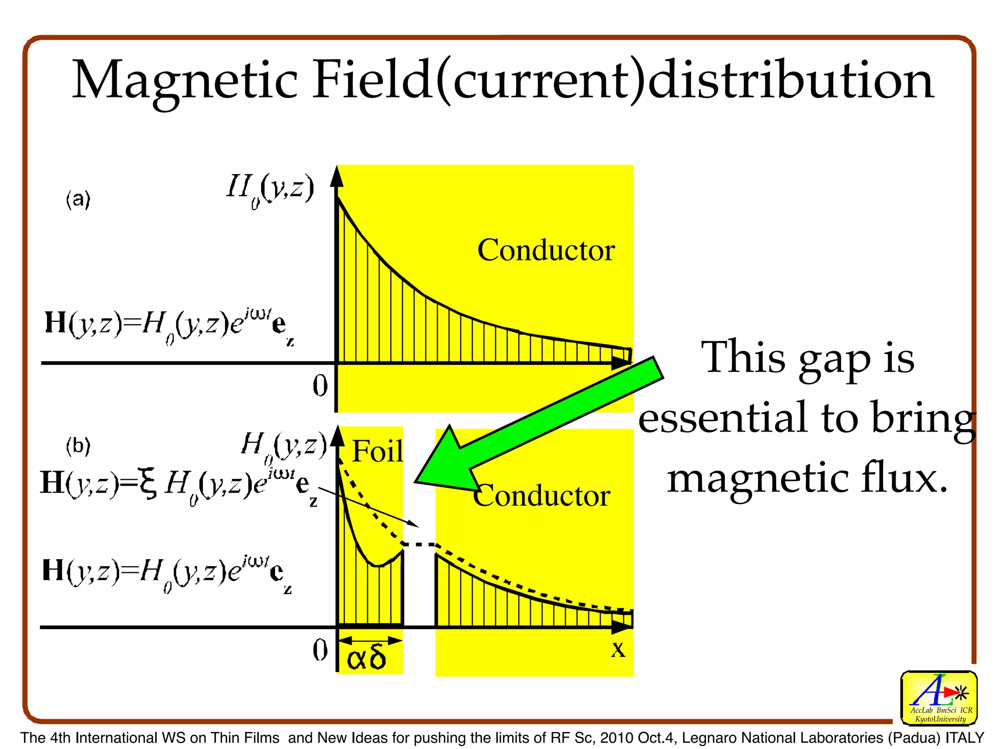
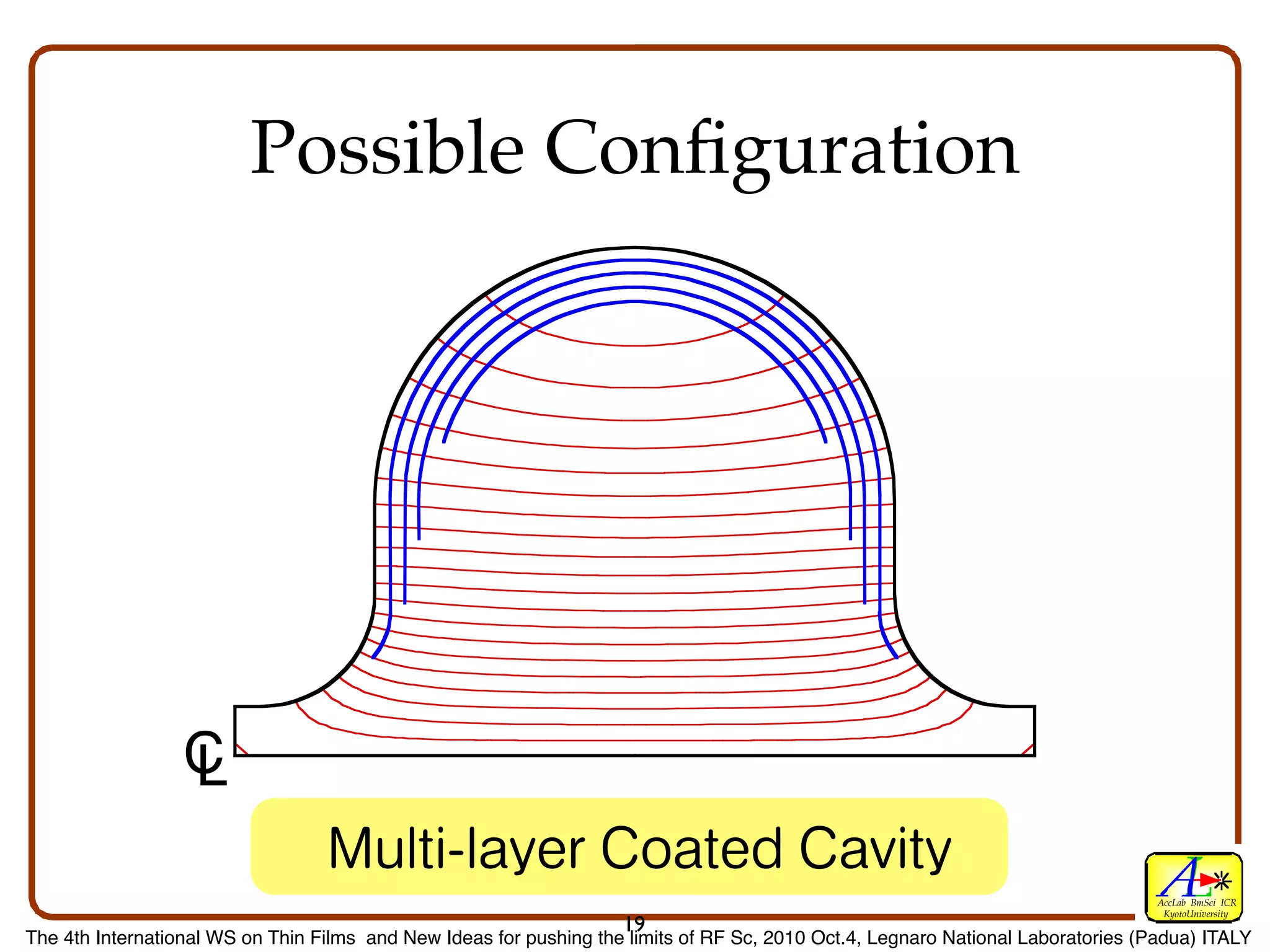
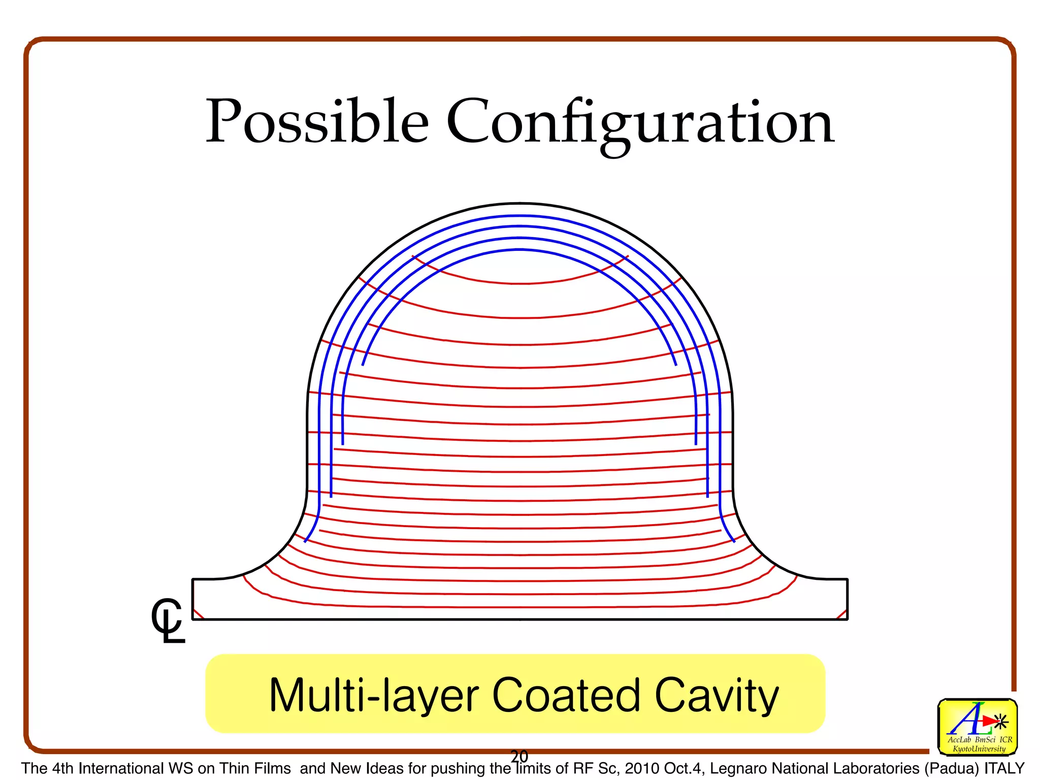

This document discusses a laminated conductor structure for radio frequency (RF) applications, emphasizing the reduction of skin-effect losses in transmission lines through proper conductivity and permeability adjustments. It includes analyses of current distribution and electromagnetic wave propagation in laminated conductors, alongside theoretical and experimental findings. The study highlights potential improvements in Q factors and the need for further investigation into the interactions of insulating layers and magnetic flux in these structures.


