Dubai Call Girls/// Hot Afternoon O525547819 Call Girls In Dubai
A Multiband Lna with Switched Loads and Wideband Input Impedance Matching
1. A Multiband LNA with Switched Loads and Wideband
Input Impedance Matching
Gustavo Pérez Ruiz, Sunil L. Khemchandani, Roberto Díaz Ortega, Rubén Pulido Medina,
Dailos Ramos Valido and Javier del Pino.
Applied Microelectronics Research Institute and Departamento de Ingeniería Electrónica y Automática, University of Las Palmas de Gran Canaria, Las Palmas, Spain
Publicated in
XXIV Design of Circuits and Integrated Systems Conference
Zaragoza, Spain (2009).
Abstract
A fully-integrated multiband low noise amplifier topology is proposed. This configuration combines a wideband input impedance
with two switched resonant circuits in the load of the amplifier. The use of reactive matching is extended to wide bandwidths
using the impedance property of LC-ladder filters. The multiband LNA is implemented in a BiCMOS 0.35 µm process. Simulations,
including technology parasitics, show a maximum gain of 16 and 12 dB at 1.8 and 2.4 GHz respectively. The minimum NF for both
frequencies are 2.5 and 3.4 dB, and the input IP3 at 1.5 GHz is 1.5 dBm. The chip size is 0.771 × 0.848 mm2 and the total power
consumption, without the output buffer, is 16 mW at 3.3 V.
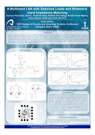
LNA Design
Measurements & Simulations
Fig. 5 S21 post-layout simulation when v18
and v24 are active Fig. 6 S11 post-layout simulation when v18
and v24 are active
Fig. 1 Simplified schematic of the LNA with wideband input impedance matching
Fig. 5. Measured inductance (solid line), Fig. 8 LNA IIP3 post-layout simulation
0
Conclusions
A multiband LNA configuration with wideband input impedance
matching has been presented. The amplifier switches two resonant
circuits to commute different frequency bands, centered at 1.8 GHz
and 2.4 GHz. The amplifier exhibits a wideband input impedance
matching, being the S11 less that -10 dB across the desired
Fig. 2. Simplified schematic of the load
of the multiband LNA Fig. 3 Schematic of the multiband LNA bandwidth. The power gain varies between 16 dB at 1.8 GHz to 12
dB at 2.4 GHz when the two resonant loads are switched. The
minimum NF for both frequencies is 2.5 and 3.4 dB, and the input
IP3 at 1.5 GHz is 1.5 dBm. Up to our knowledge, this combination
of wideband input impedance matching and switched loads has
never been used in multiband LNAs. The circuit was implemented
in a standard low cost BiCMOS 0.35 µm process and delivered to
the foundry for fabrication.
Acknowledgments
This work is partially supported by the Spanish Ministry of Science and
Innovation (TEC2008-06881-C03-01) and the Spanish Ministry of Industry,
Tourism and Trade (TSI-020400-2008-71).
Fig. 4 Layout of the multiband LNA
INSTITUTO UNIVERSITARIO DE MICROELECTRÓNICA APLICADA (IUMA)
UNIVERSIDAD DE LAS PALMAS DE GRAN CANARIA (ULPGC)