Download as PDF, PPTX

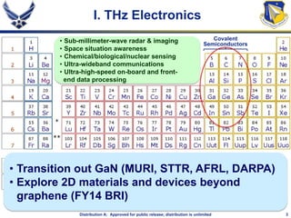

The document provides an overview of research and advancements in GHz-THz electronics, focusing on breakthroughs in materials and devices for transistors and reconfigurable electronics. It discusses challenges in perfecting crystalline structures, material purity, and the understanding of interactions at the nanoscale. Key topics include 2D materials beyond graphene, novel semiconductors, and the metal-insulator transition properties in various oxides.