Download as PDF, PPTX
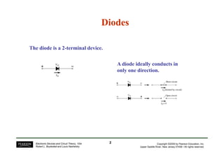
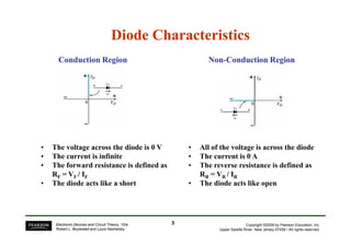
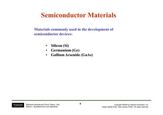


The document summarizes key concepts about semiconductor diodes. It discusses how diodes are made from doped semiconductor materials like silicon and conduct current mainly in one direction. Diodes have different operating characteristics depending on whether they are forward biased, reverse biased, or at no bias. The document also covers diode testing methods and applications of diodes like in LEDs and zener diodes.


