Downloaded 176 times

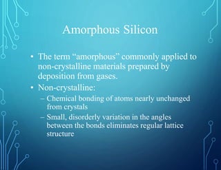
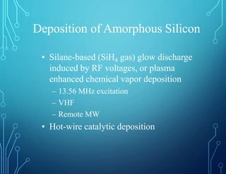
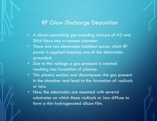
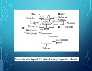
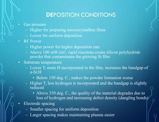
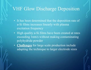

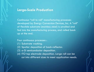
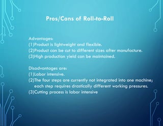


The document discusses various fabrication techniques for amorphous silicon solar cells. It describes how amorphous silicon is deposited through plasma enhanced chemical vapor deposition (PECVD) using silane gas and how hydrogen is essential to improving the material's electronic properties. It also discusses large-scale roll-to-roll manufacturing processes and compares advantages of amorphous silicon like deposition on different substrates to disadvantages like lower efficiency compared to crystalline silicon.


