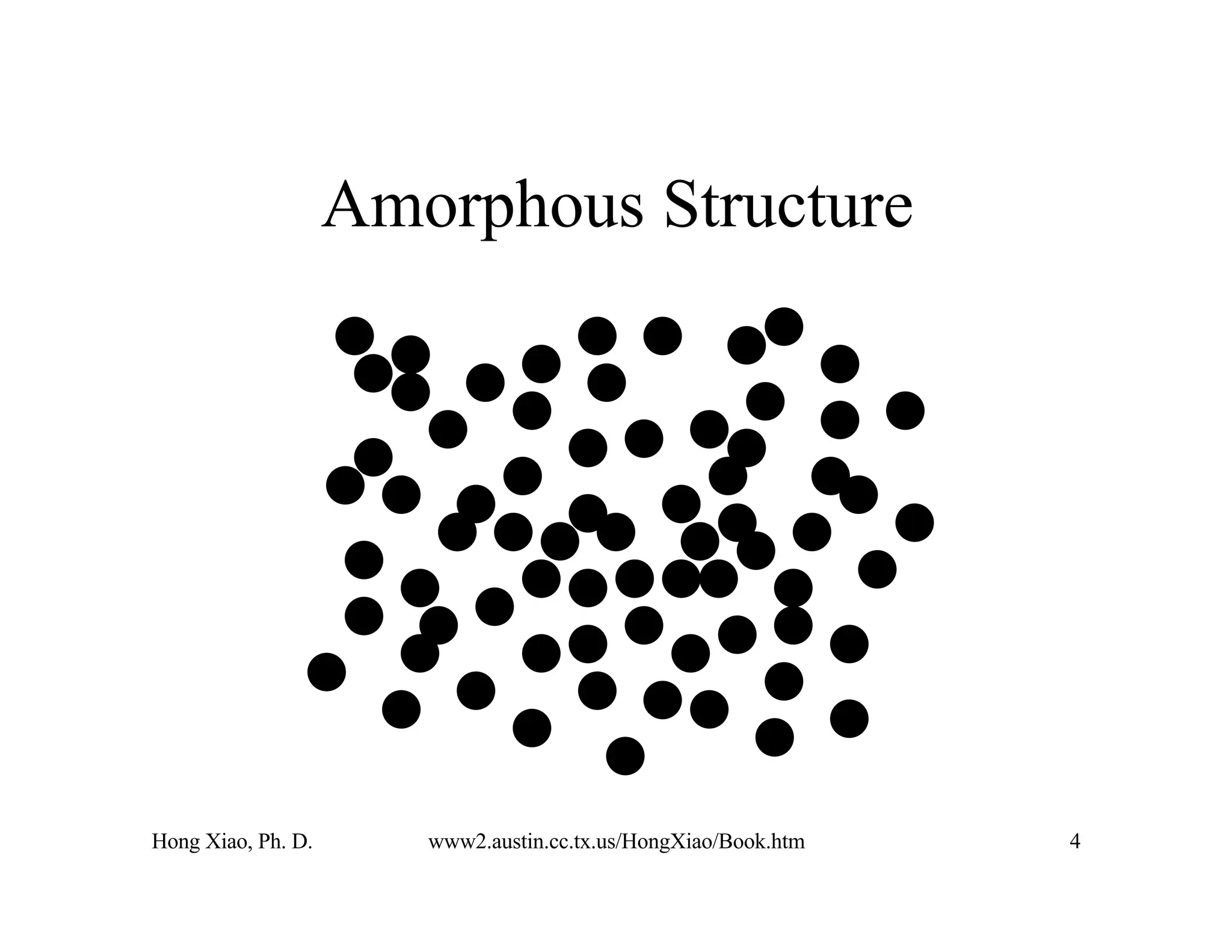
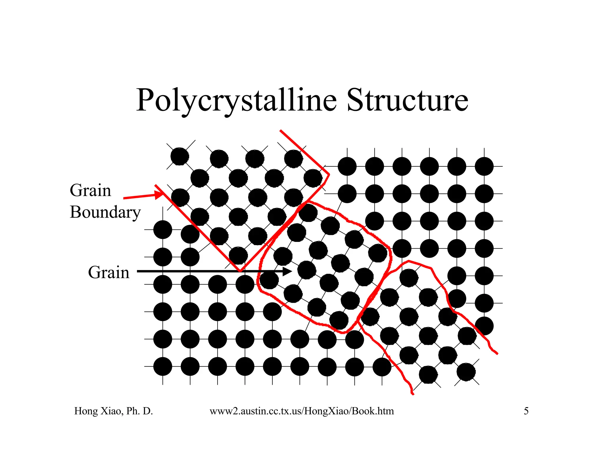
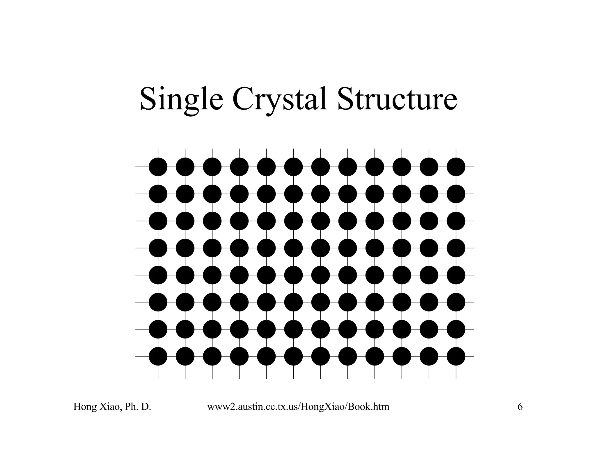
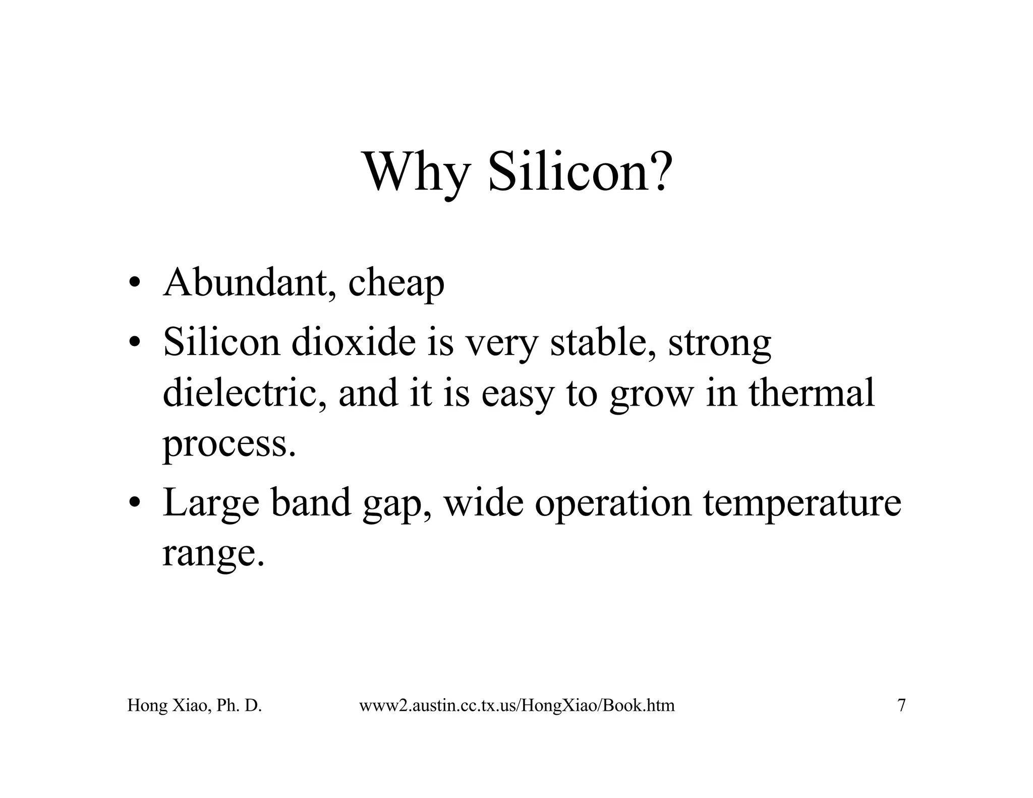
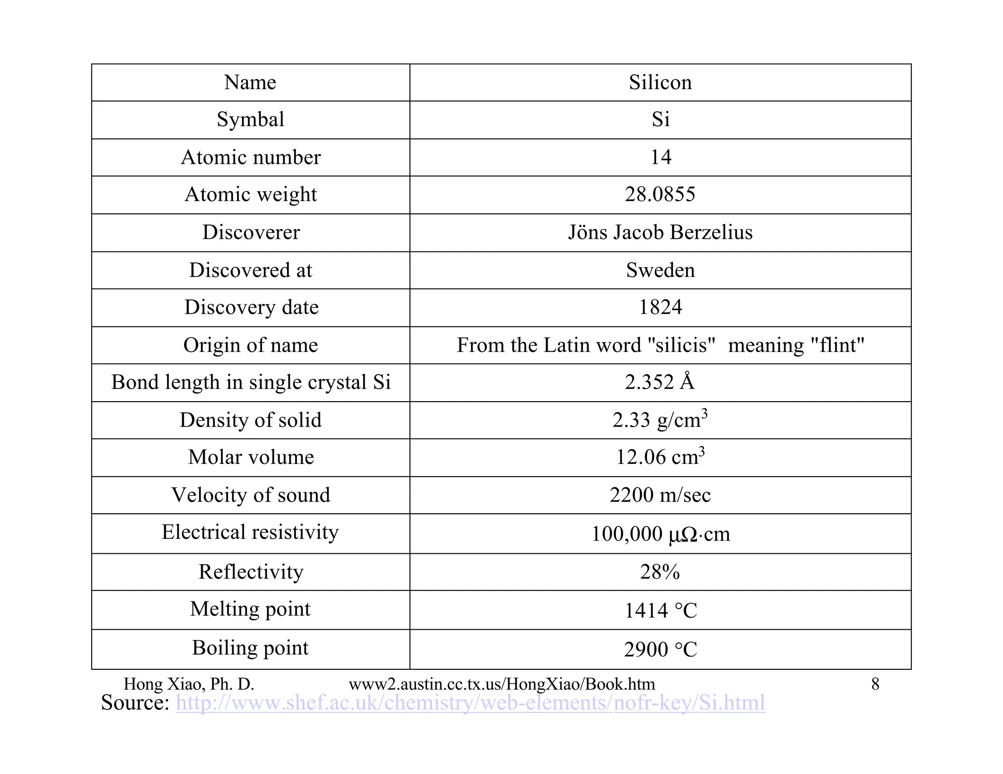
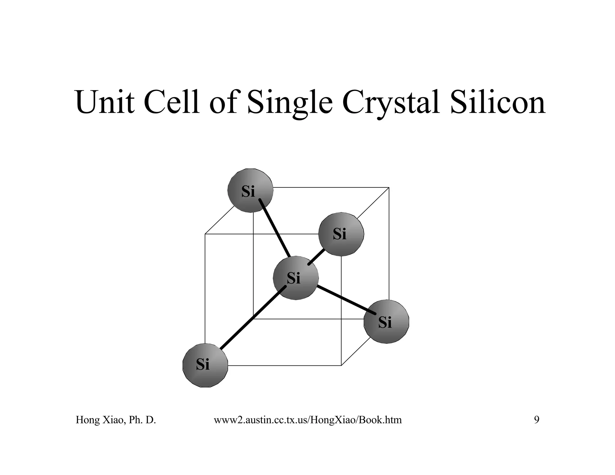
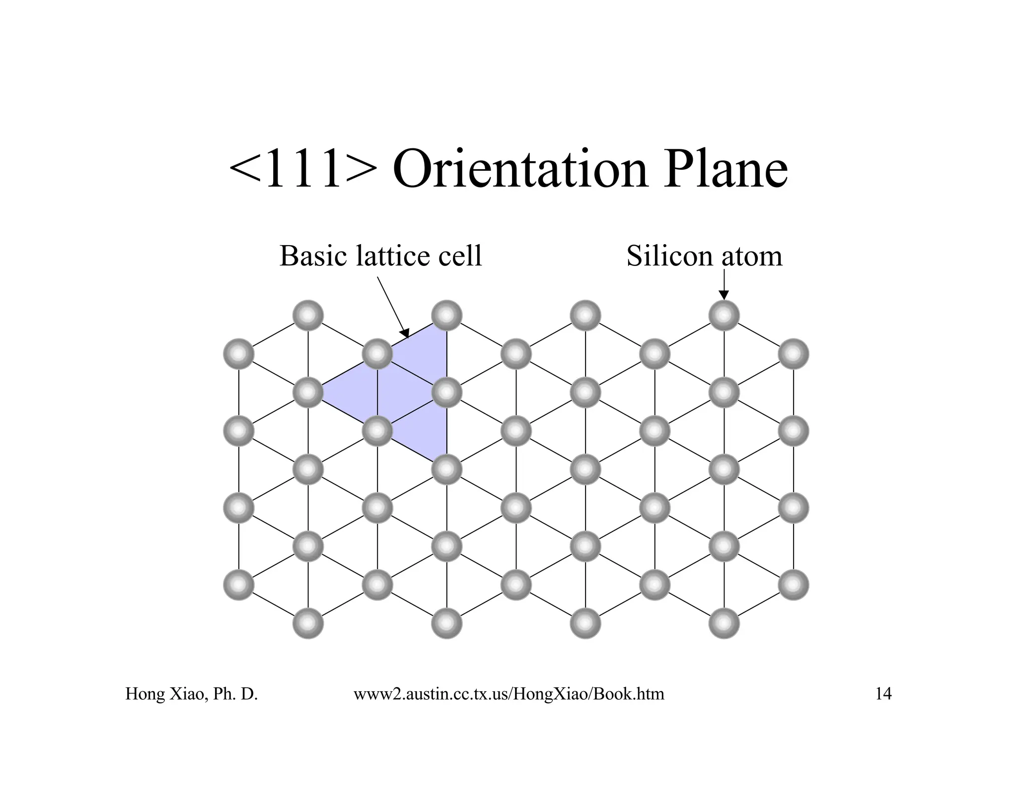
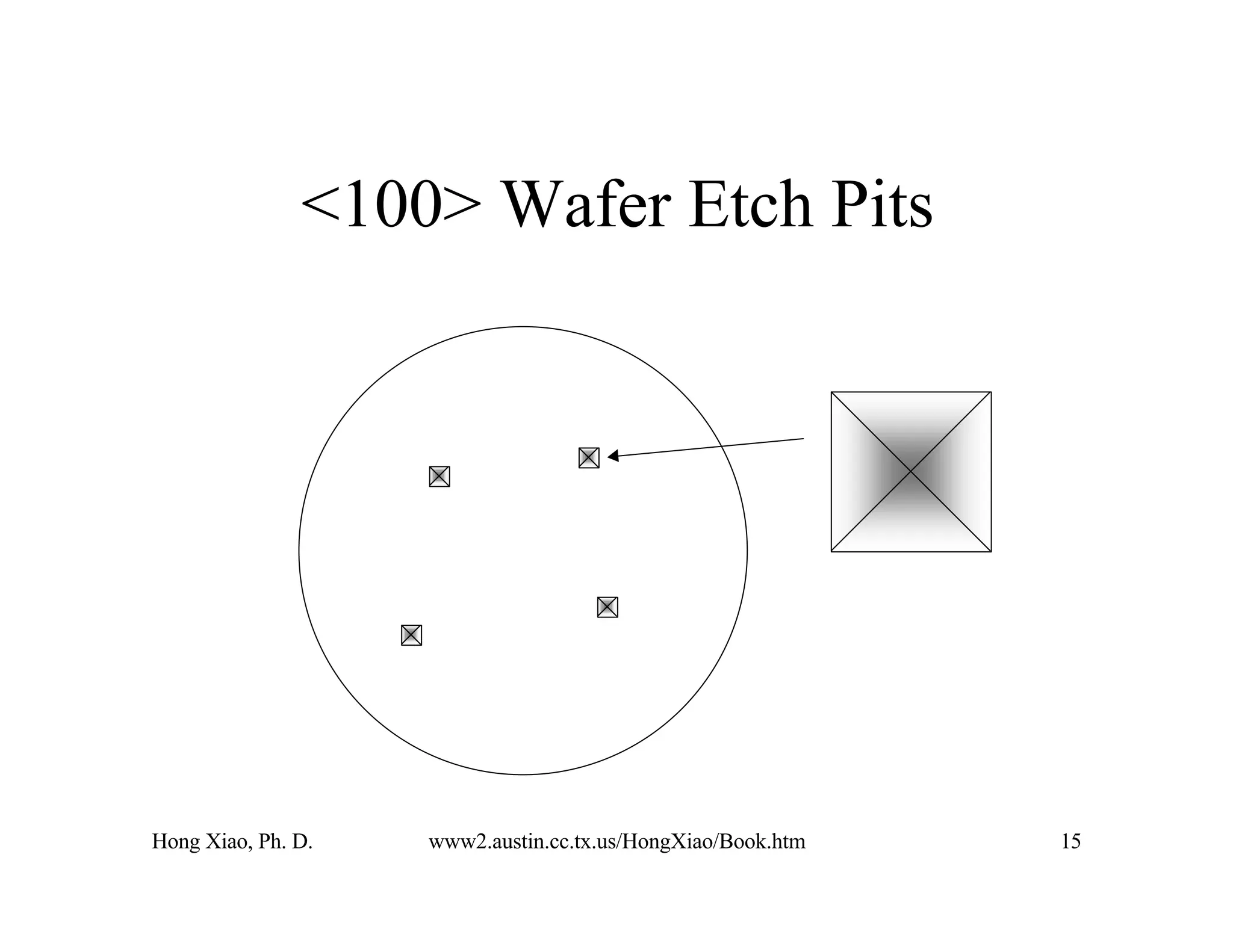
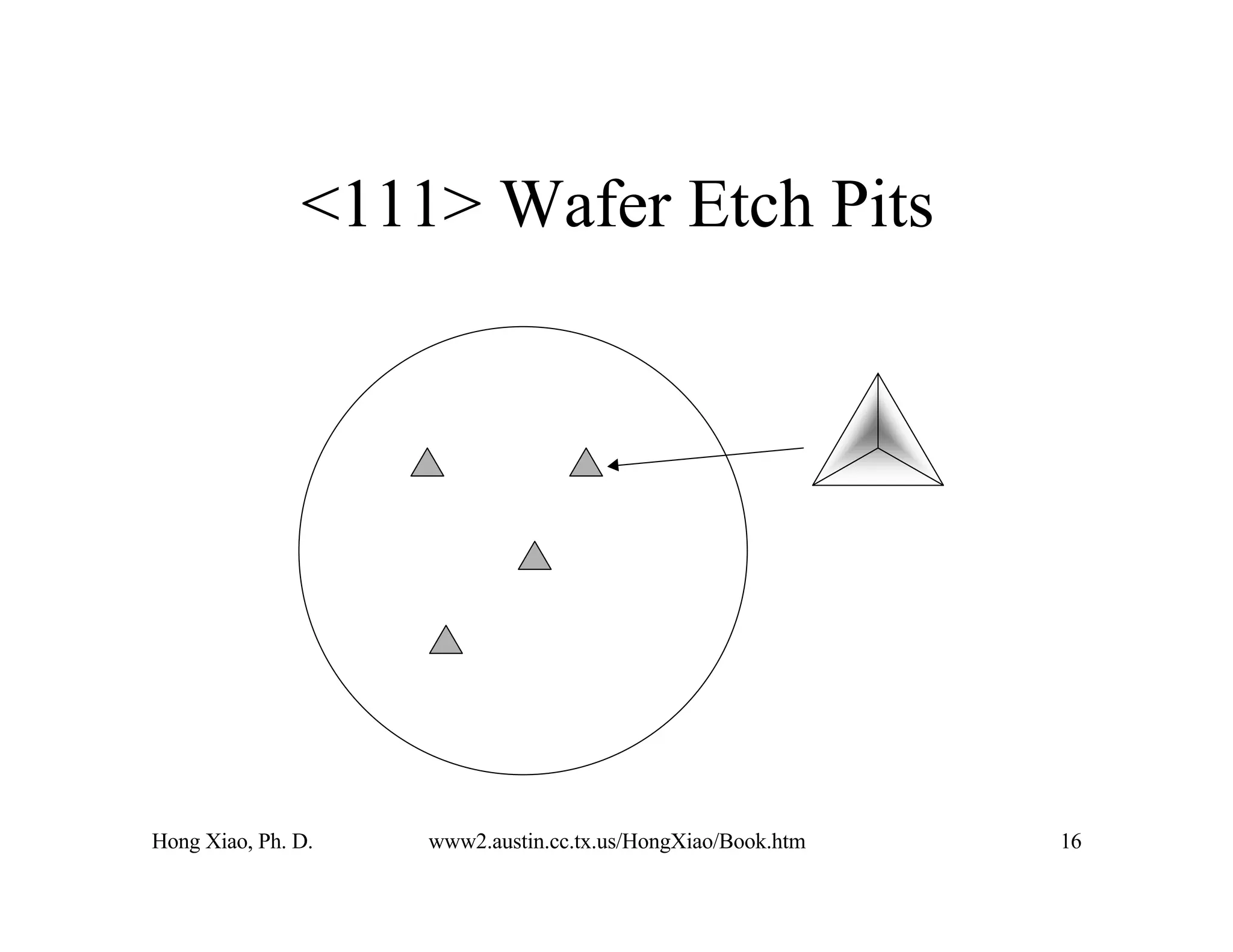
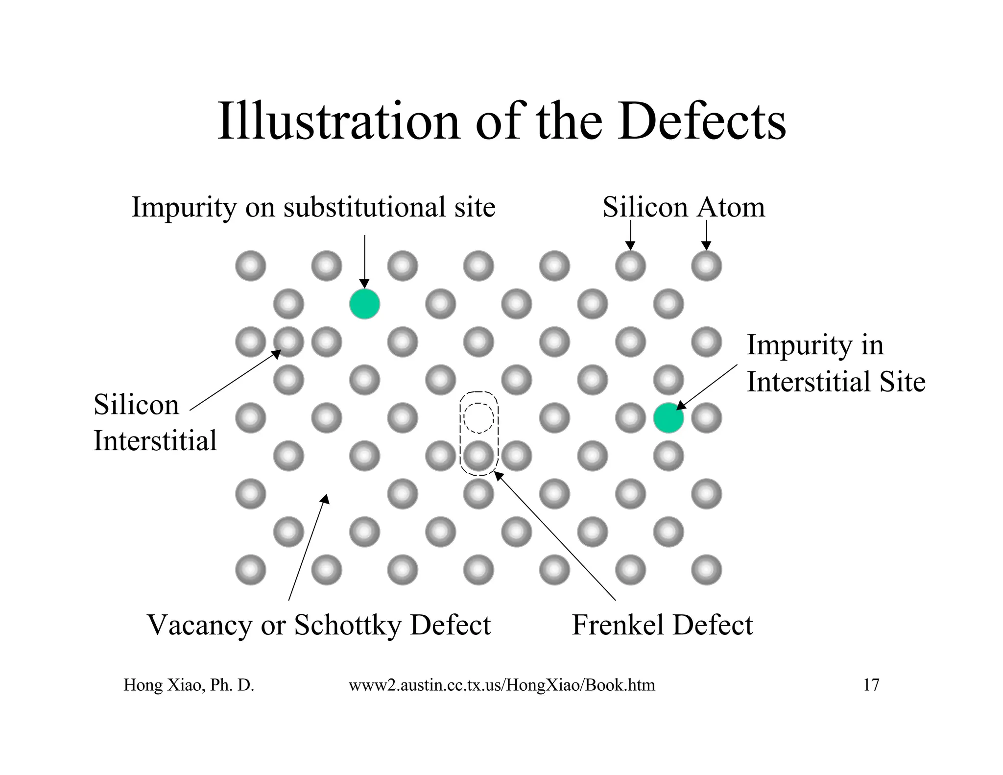
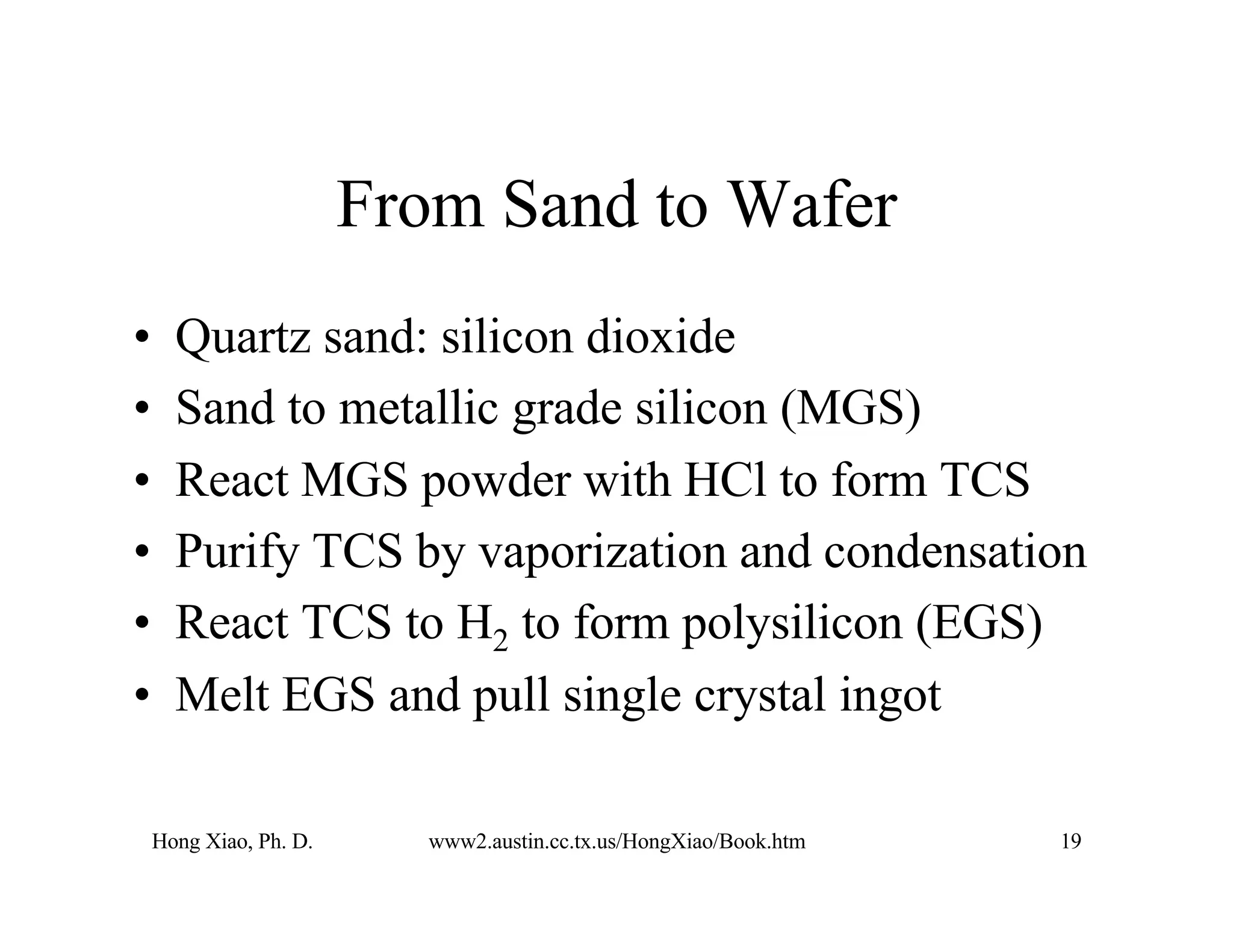
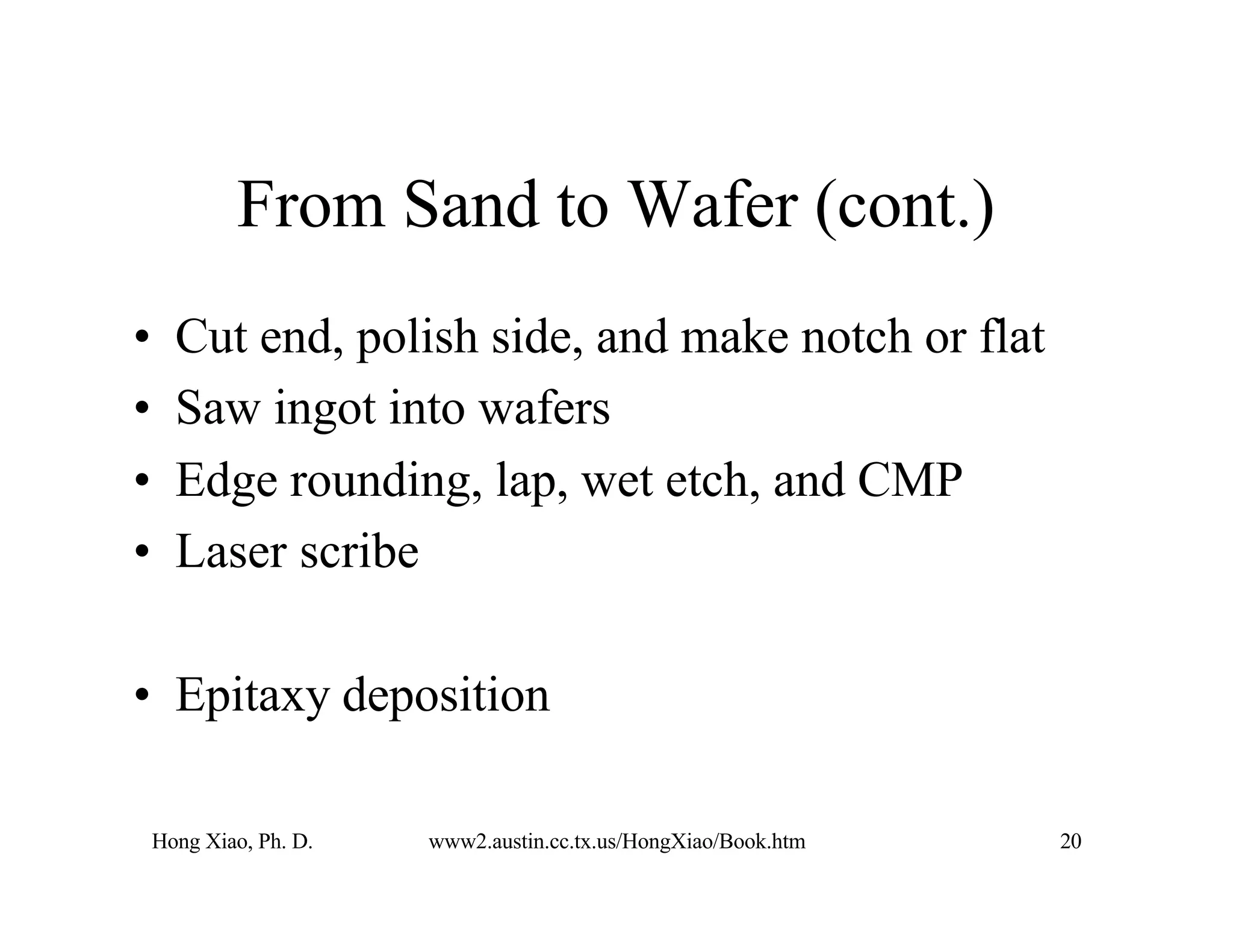
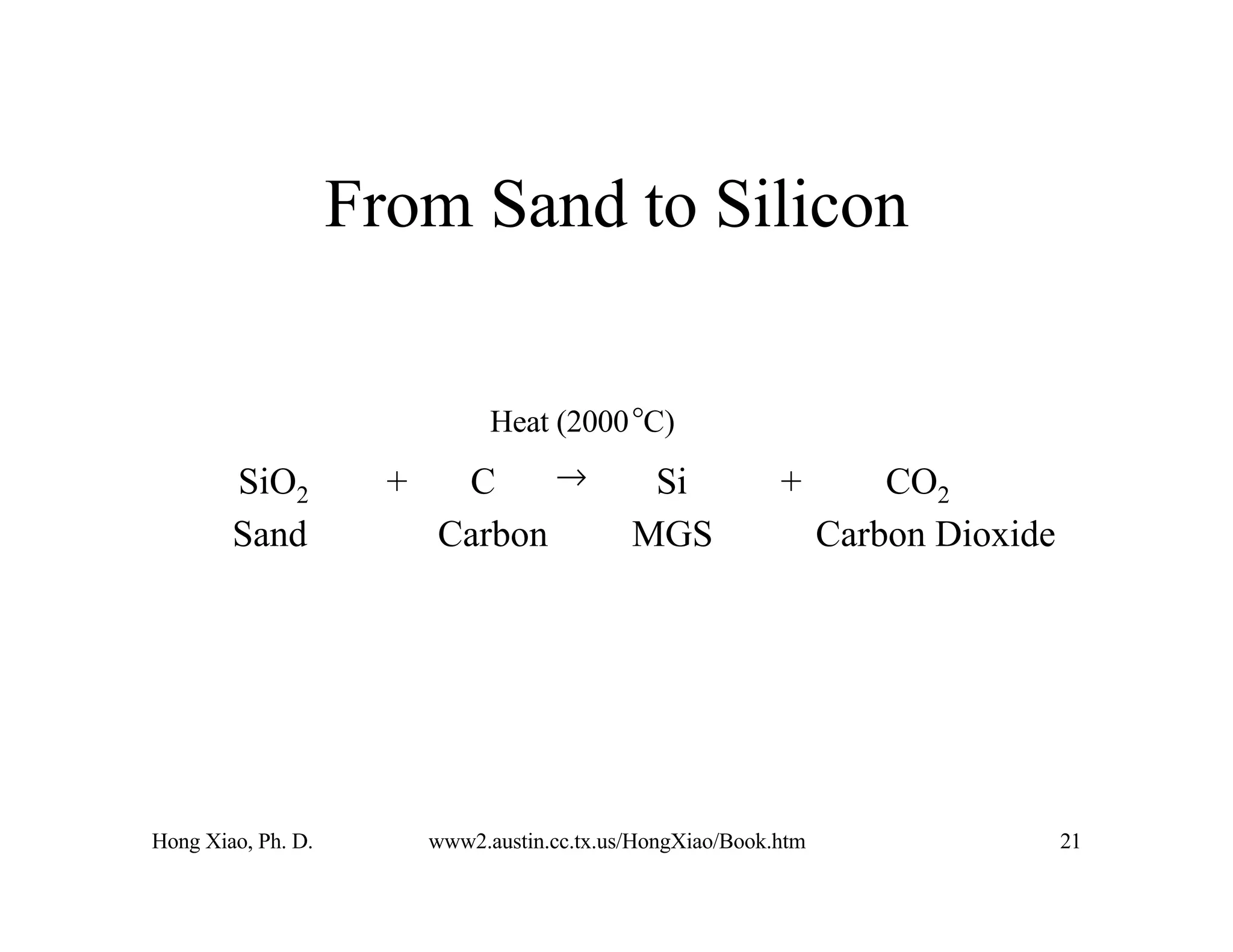
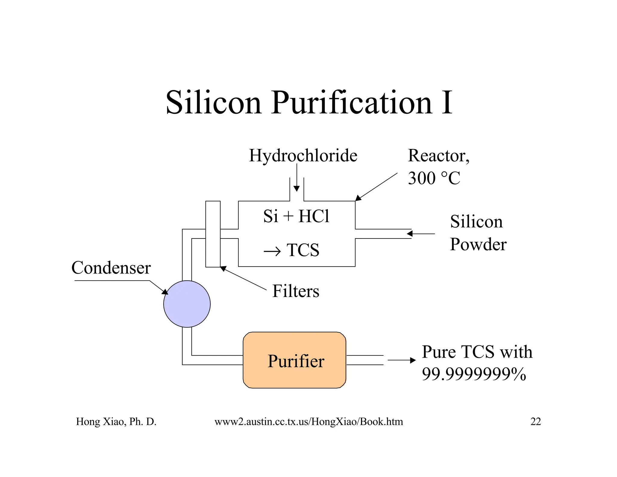
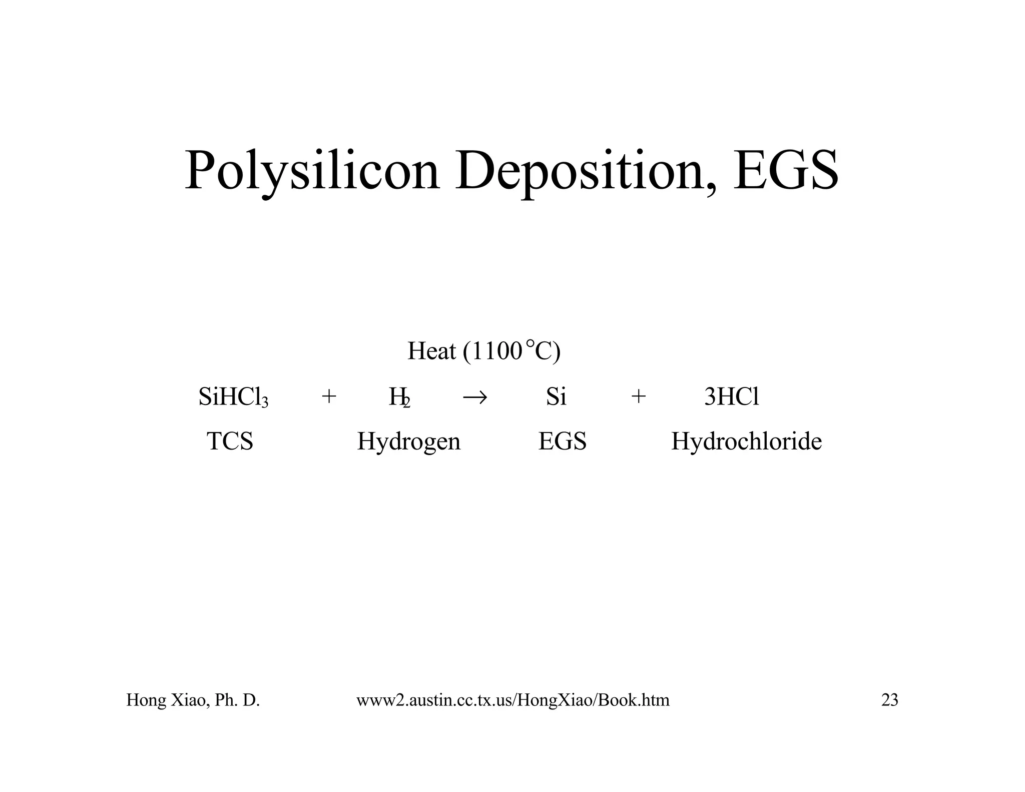
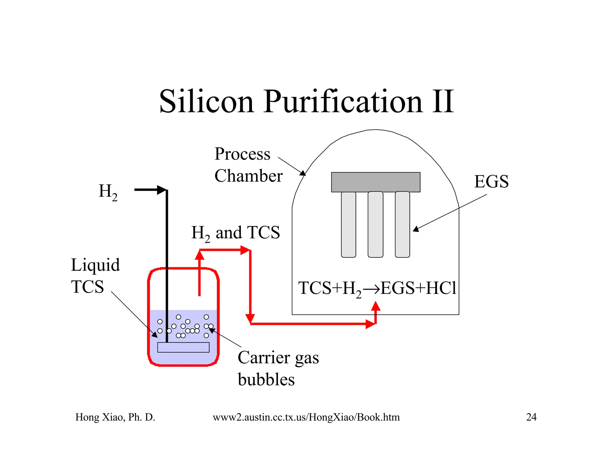
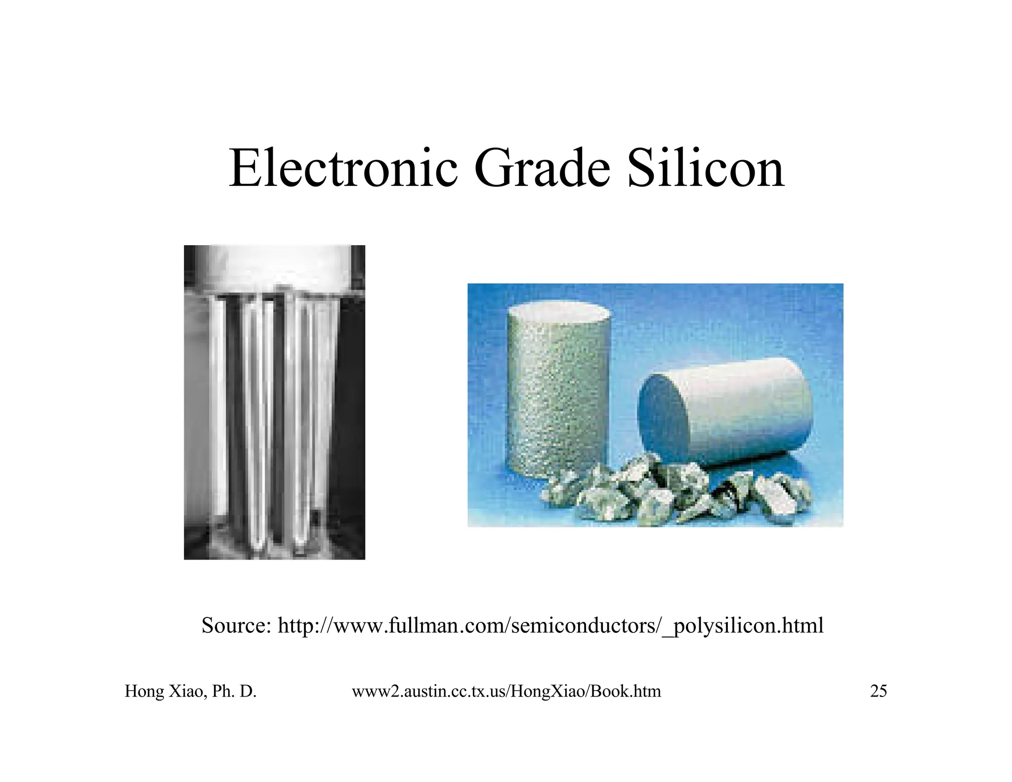
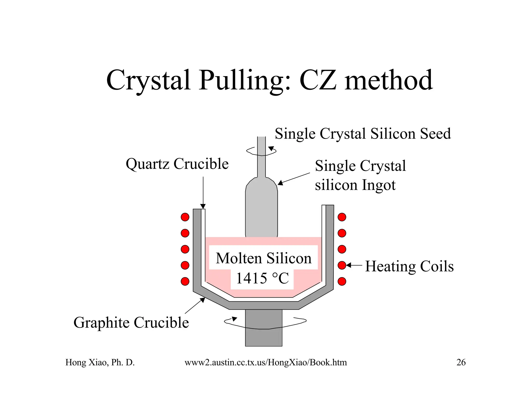
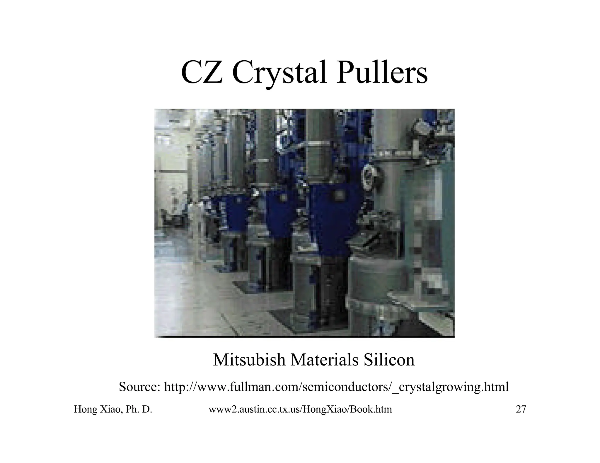
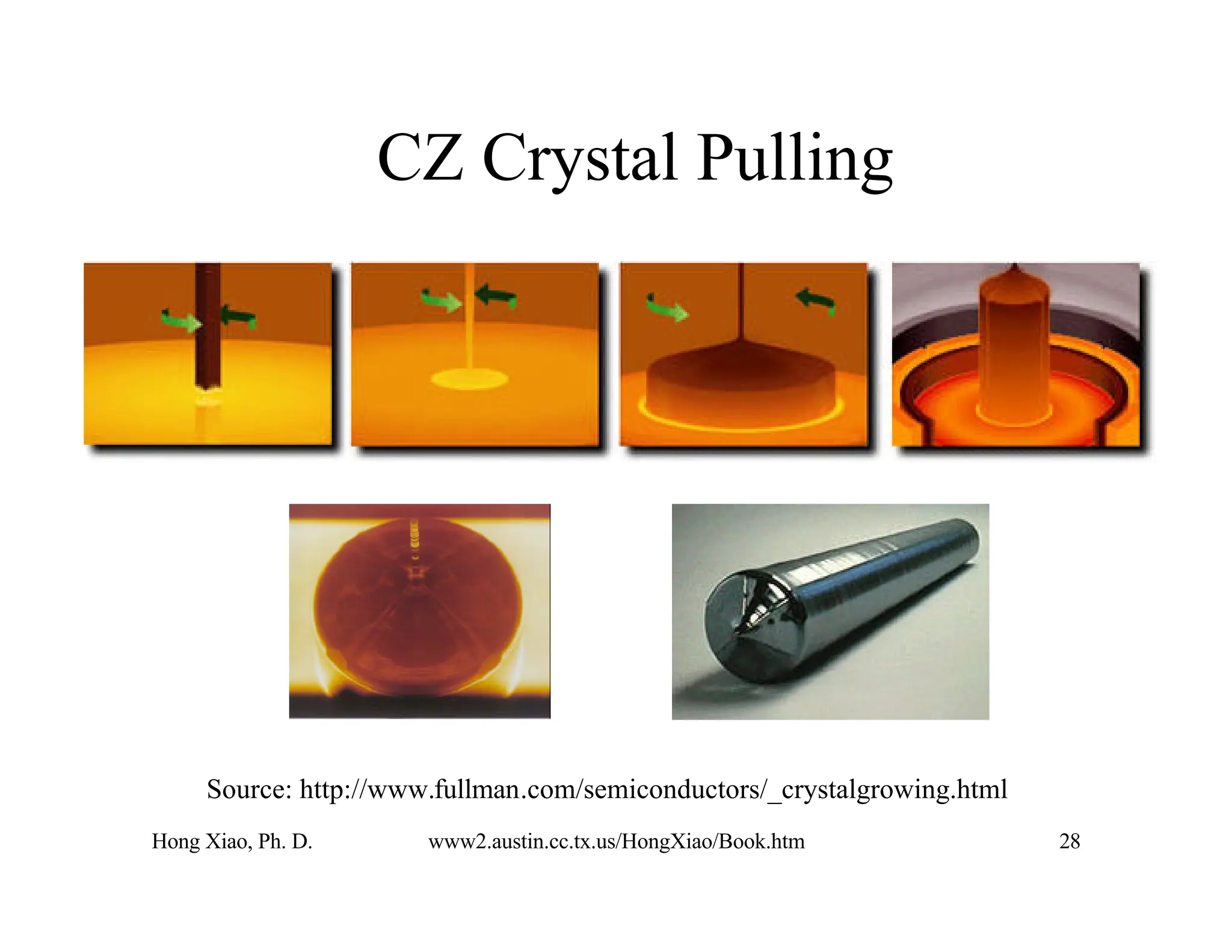
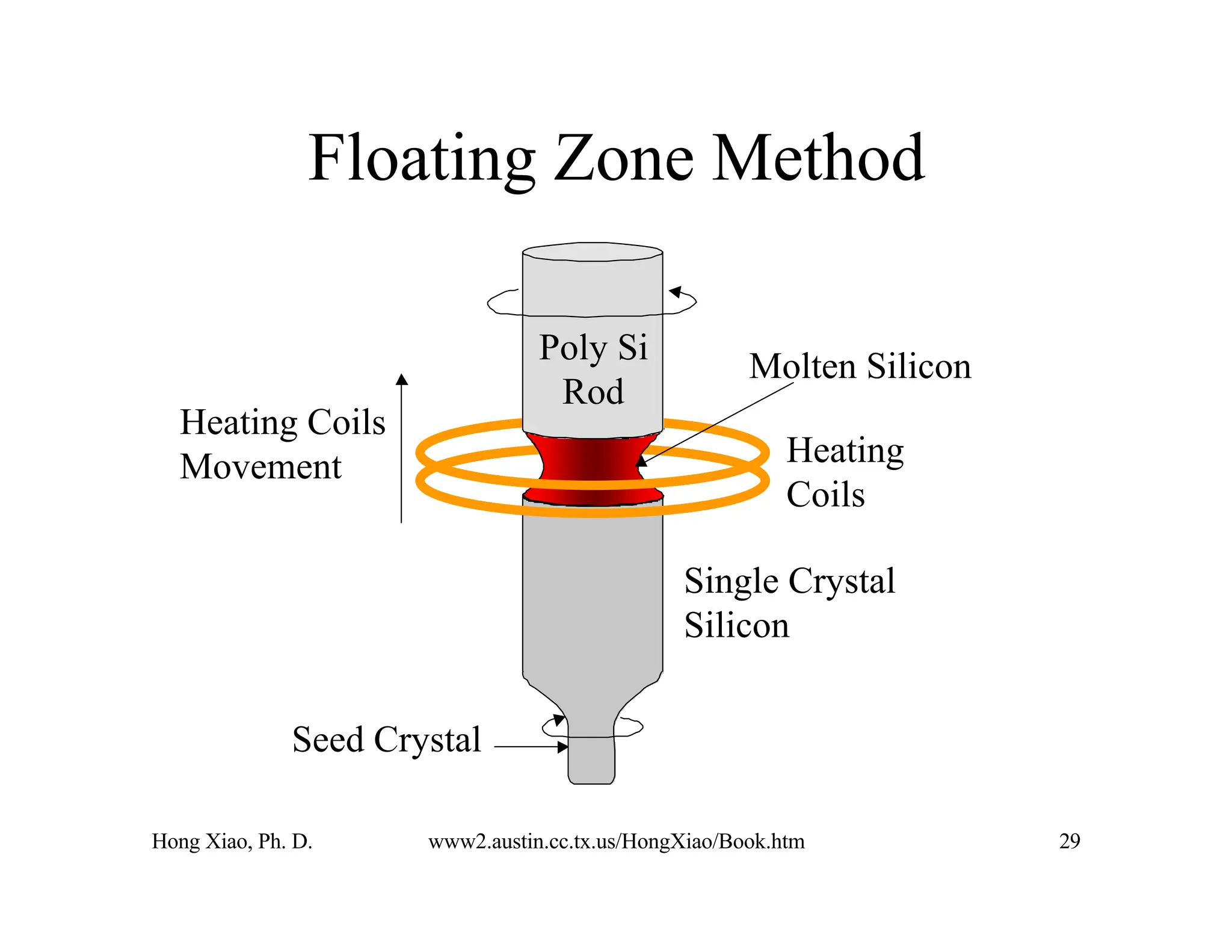
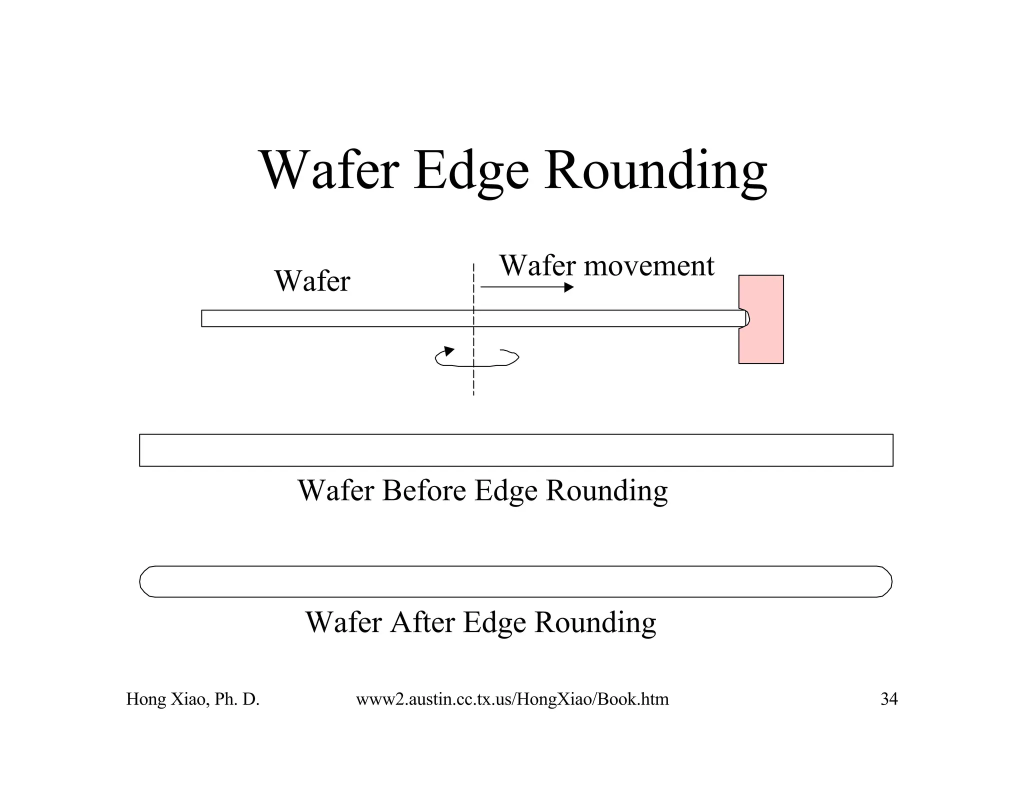
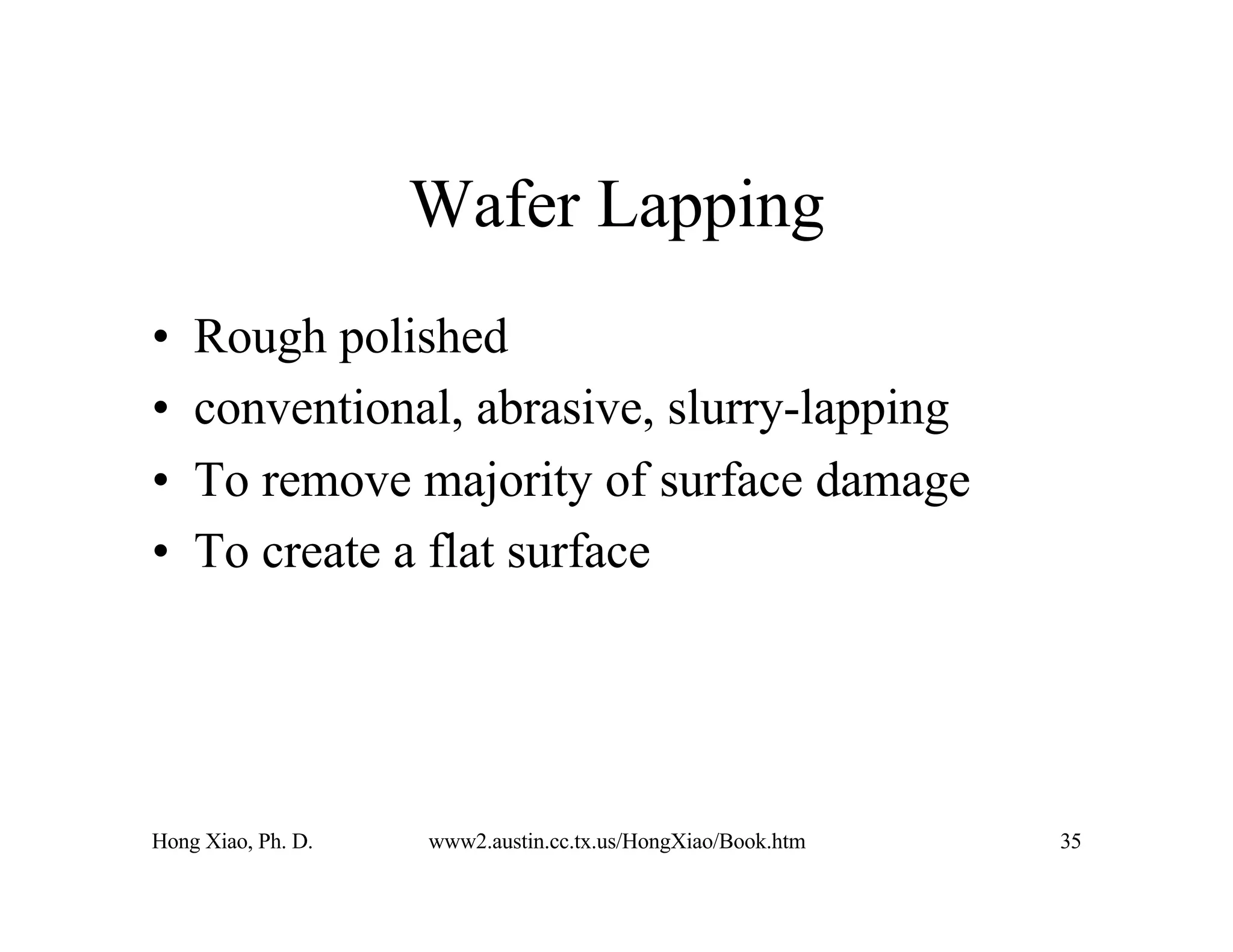
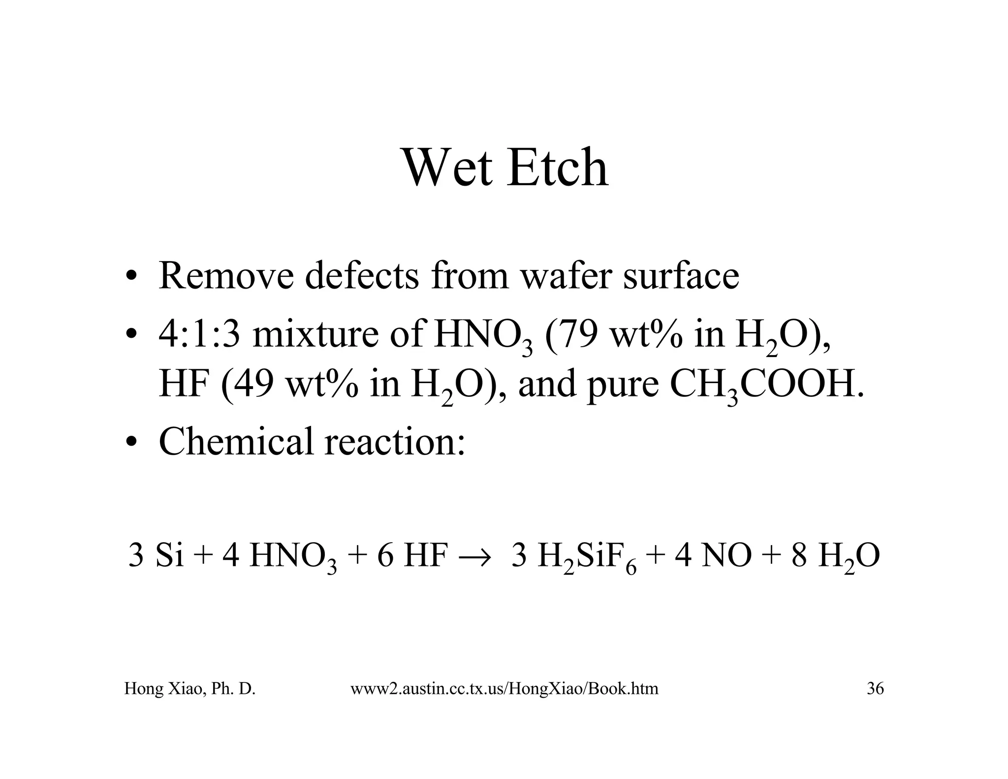
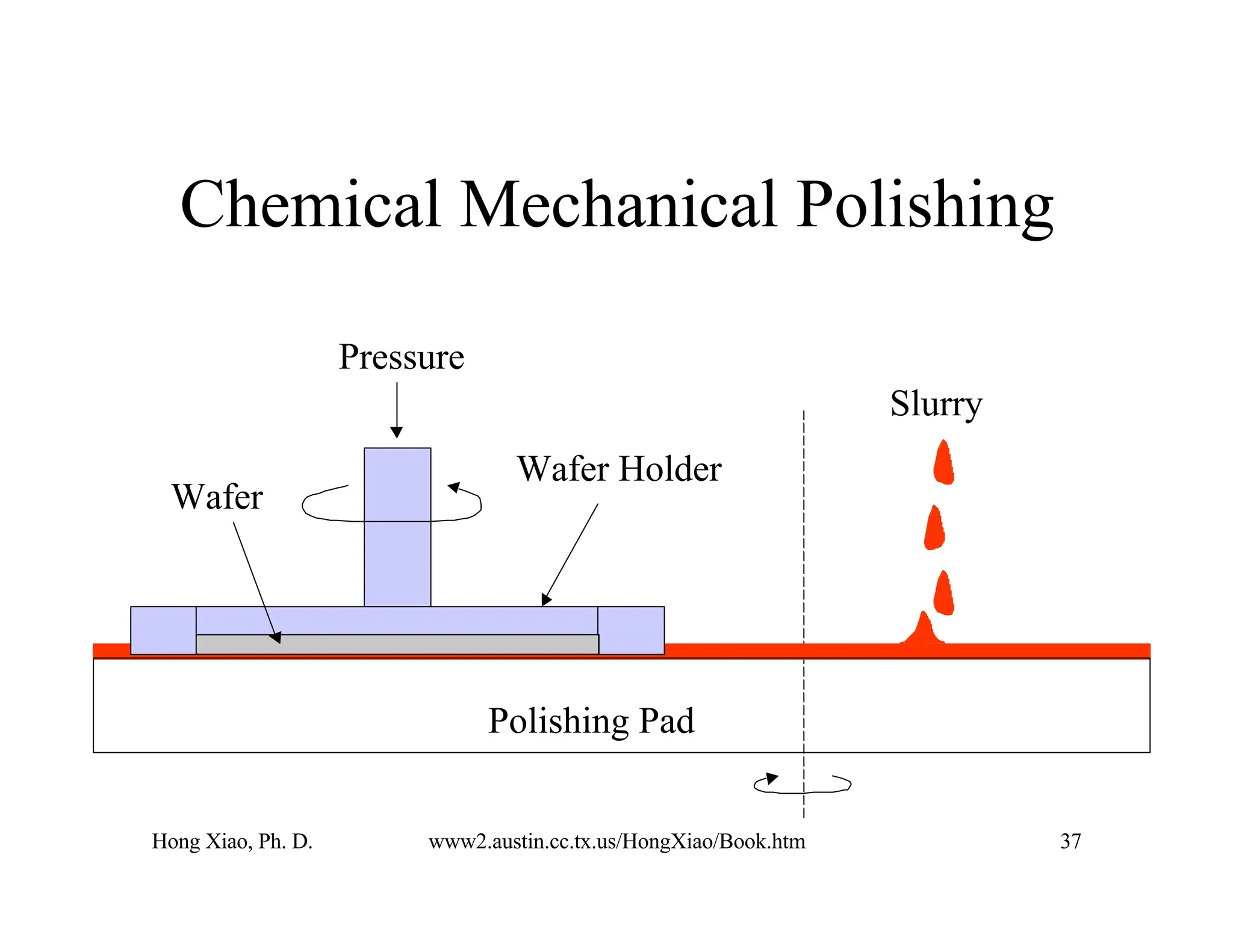
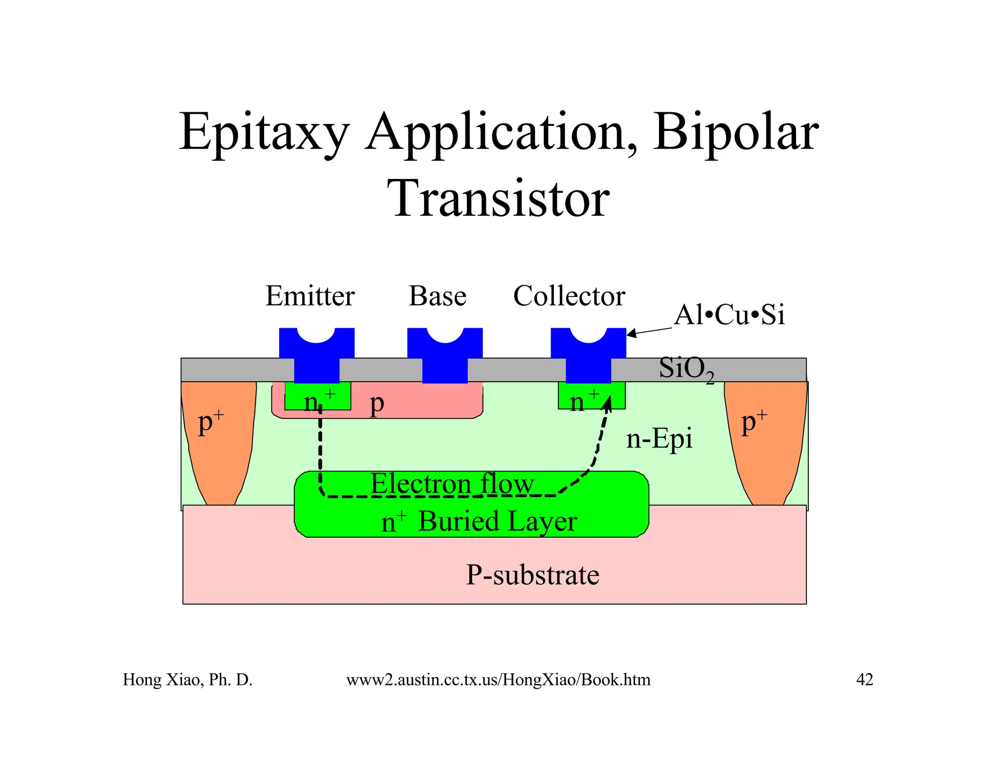
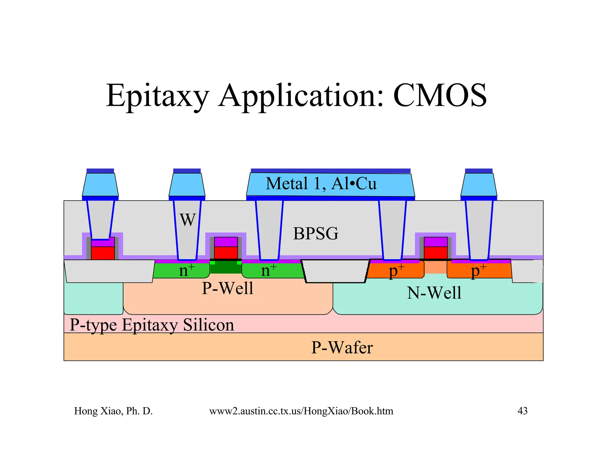
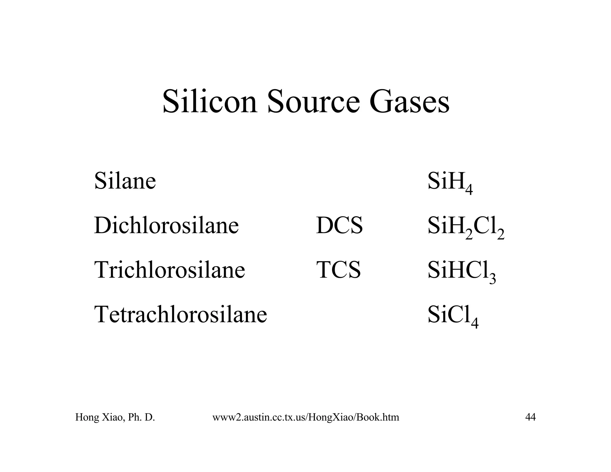
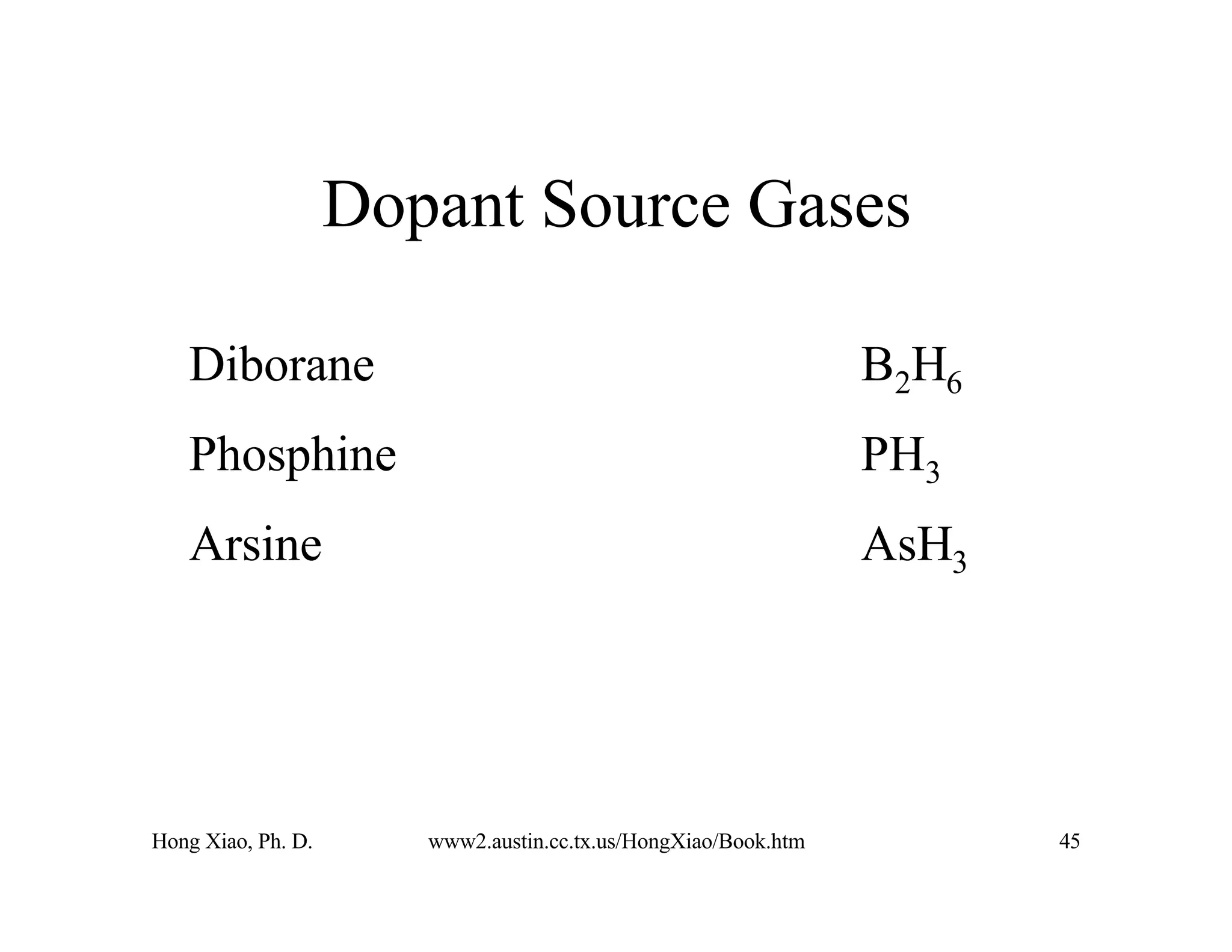
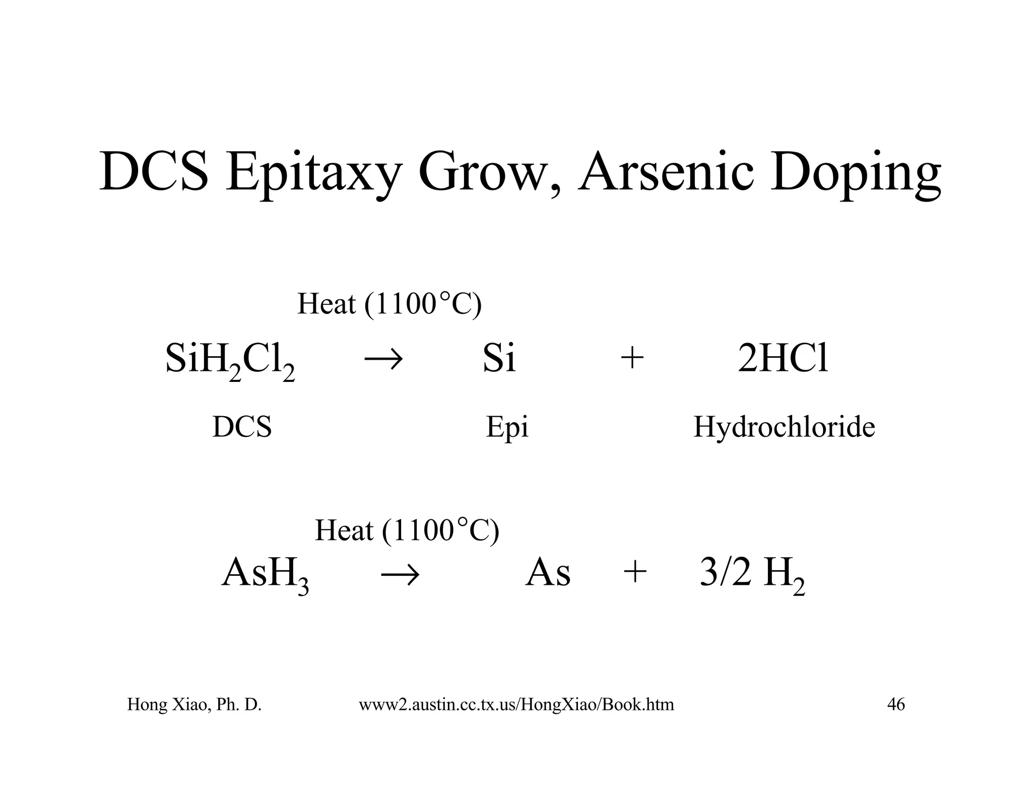
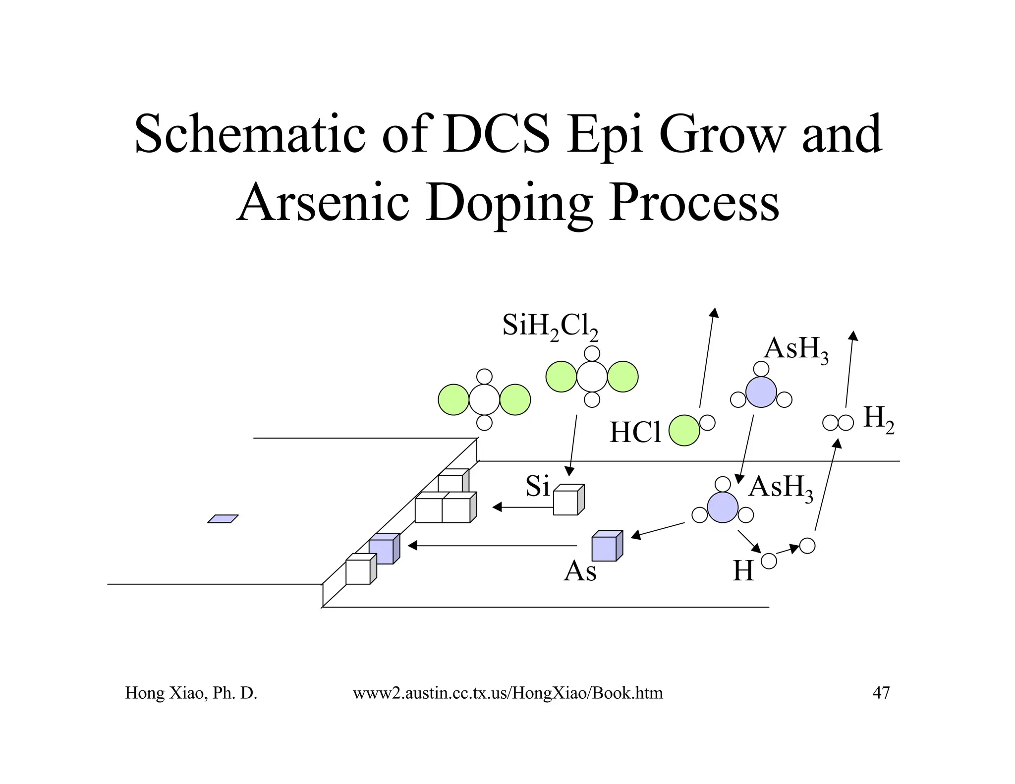
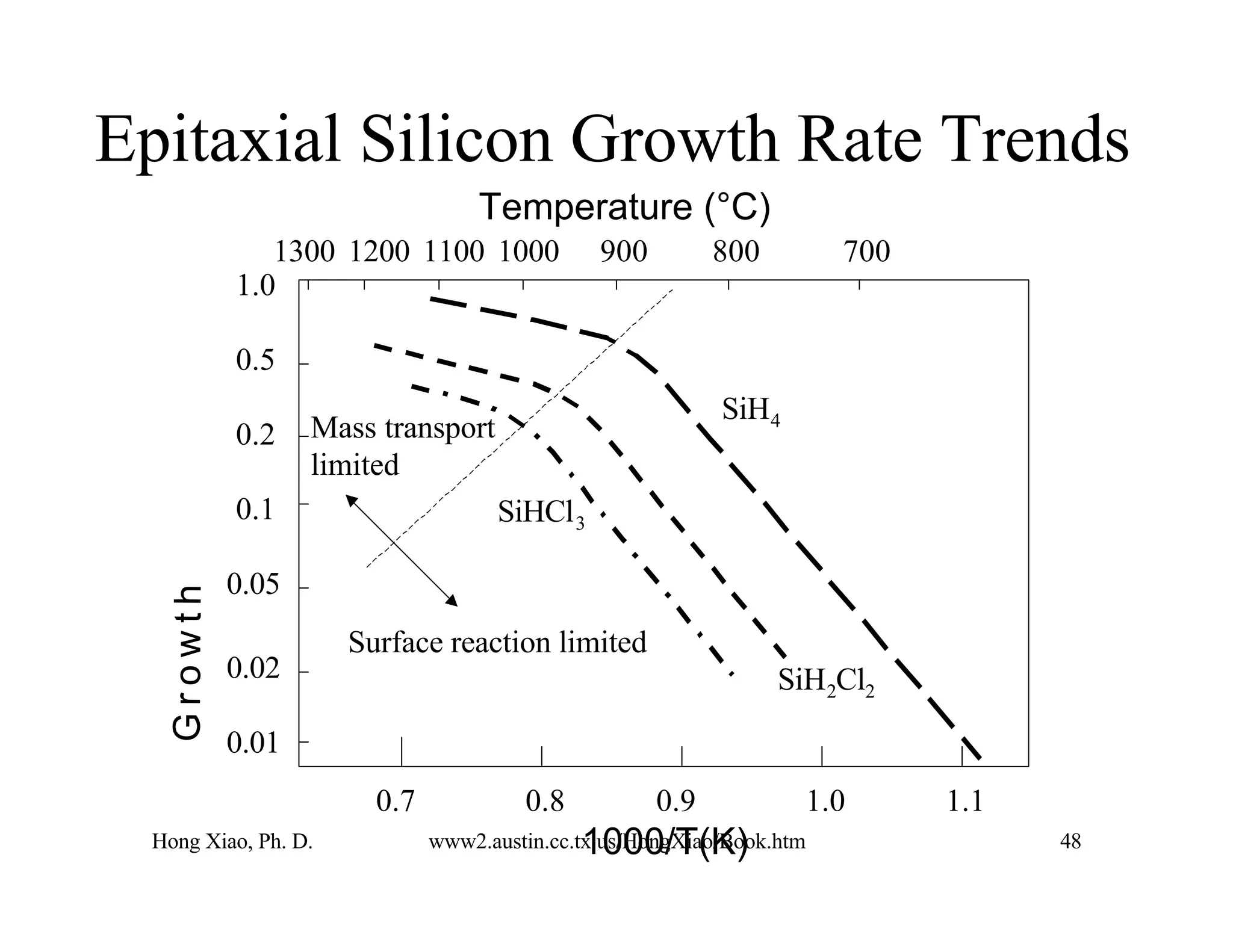
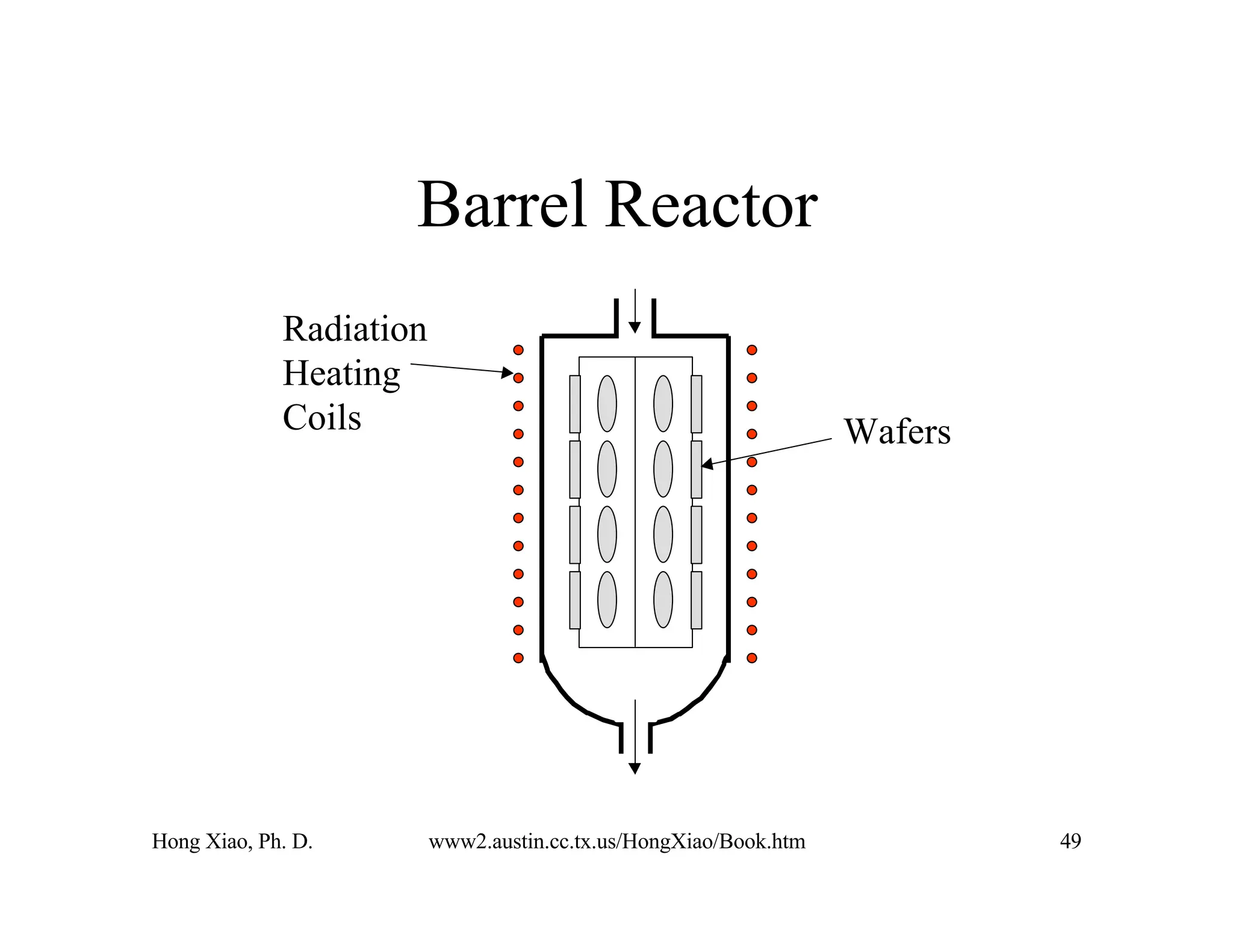
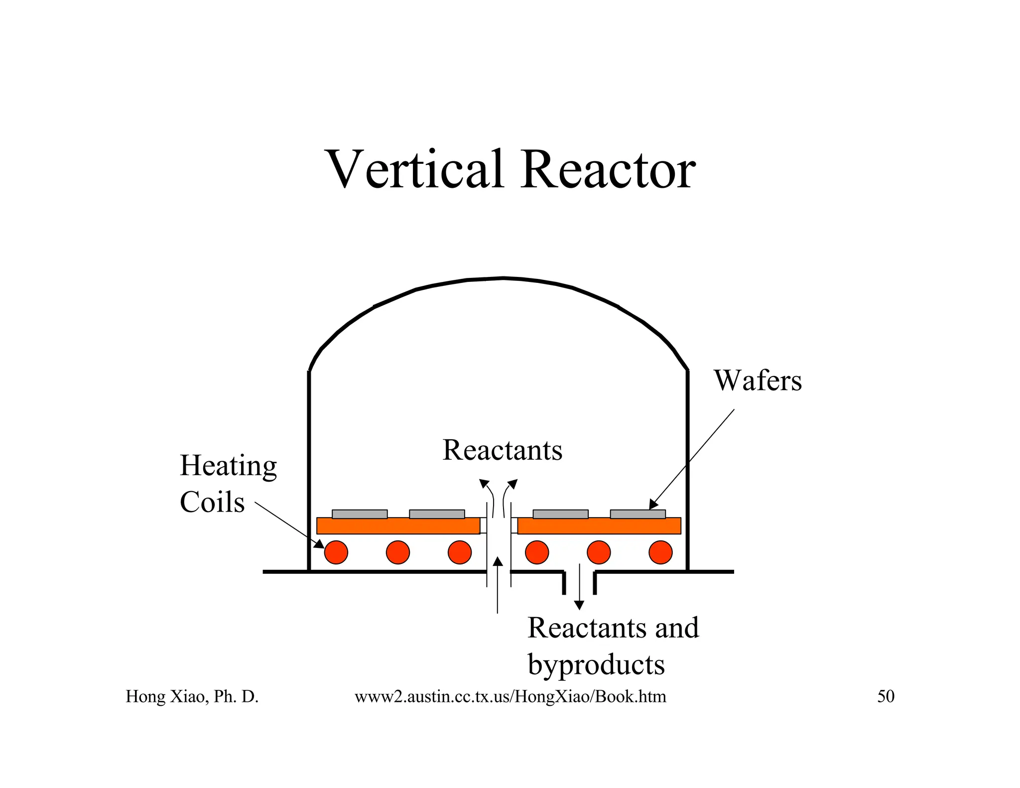
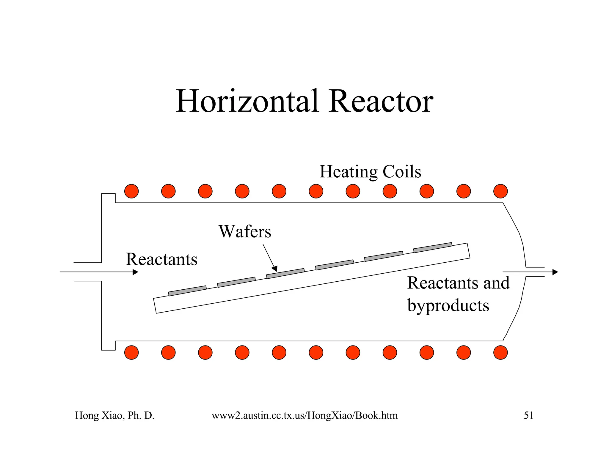
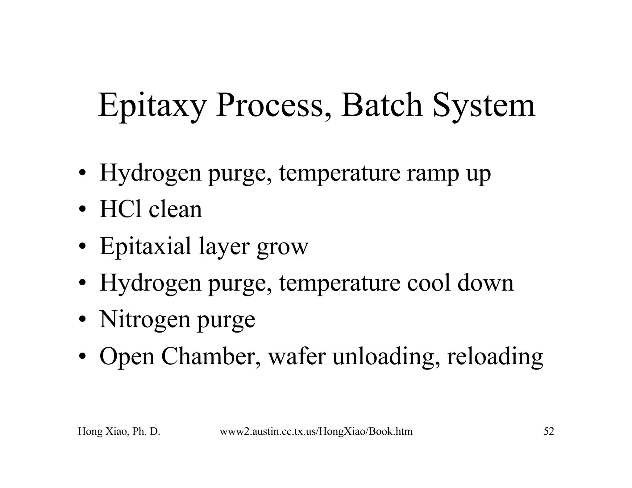
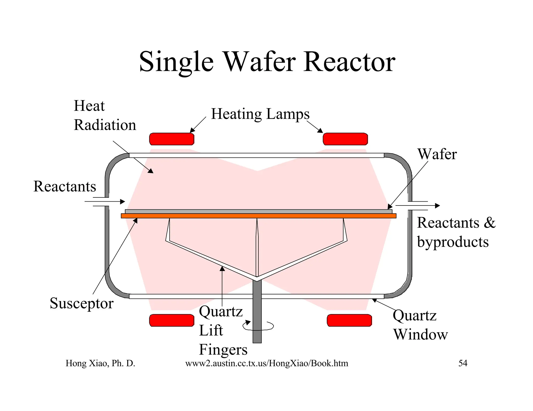
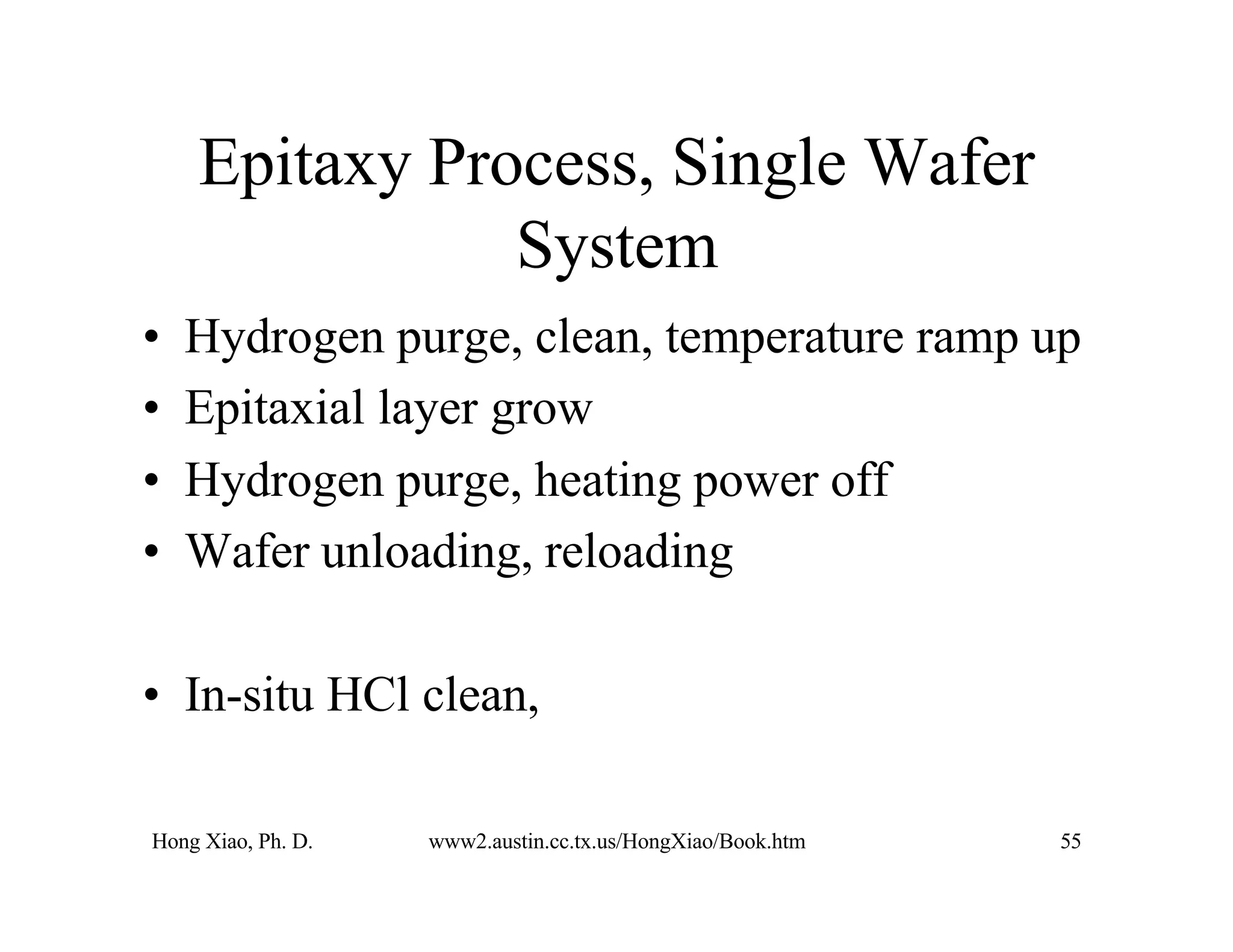
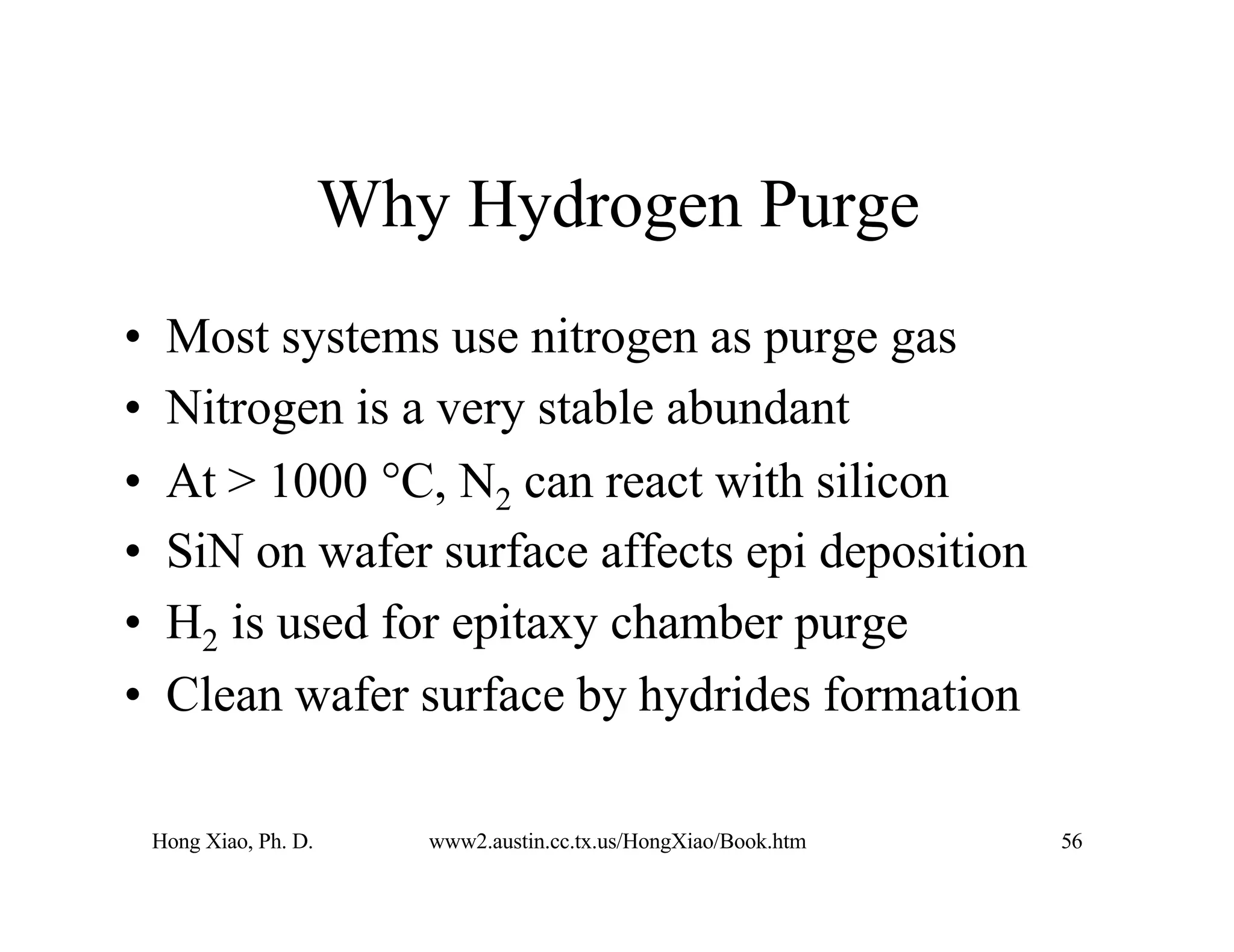
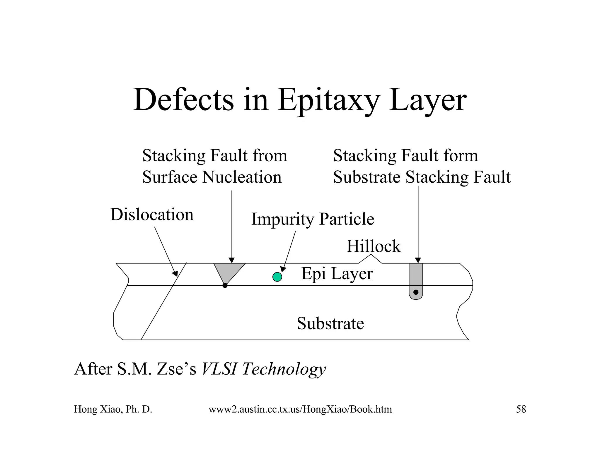
Hong Xiao, Ph. D. www2.austin.cc.tx.us/HongXiao/Book.htm 1
Chapter 4
Wafer Manufacturing
and Epitaxy Growing
Hong Xiao, Ph. D.
hxiao89@hotmail.com
Hong Xiao, Ph. D. www2.austin.cc.tx.us/HongXiao/Book.htm 2
Objectives
• Give two reasons why silicon dominate
• List at least two wafer orientations
• List the basic steps from sand to wafer
• Describe the CZ and FZ methods
• Explain the purpose of epitaxial silicon
• Describe the epi-silicon deposition process.
Hong Xiao, Ph. D. www2.austin.cc.tx.us/HongXiao/Book.htm 3
Crystal Structures
• Amorphous
– No repeated structure at all
• Polycrystalline
– Some repeated structures
• Single crystal
– One repeated structure
Hong Xiao, Ph. D. www2.austin.cc.tx.us/HongXiao/Book.htm 4
Amorphous Structure
Hong Xiao, Ph. D. www2.austin.cc.tx.us/HongXiao/Book.htm 5
Polycrystalline Structure
Grain
Grain
Boundary
Hong Xiao, Ph. D. www2.austin.cc.tx.us/HongXiao/Book.htm 6
Single Crystal Structure
Hong Xiao, Ph. D. www2.austin.cc.tx.us/HongXiao/Book.htm 7
Why Silicon?
• Abundant, cheap
• Silicon dioxide is very stable, strong
dielectric, and it is easy to grow in thermal
process.
• Large band gap, wide operation temperature
range.
Hong Xiao, Ph. D. www2.austin.cc.tx.us/HongXiao/Book.htm 8
Name Silicon
Symbal Si
Atomic number 14
Atomic weight 28.0855
Discoverer Jöns Jacob Berzelius
Discovered at Sweden
Discovery date 1824
Origin of name From the Latin word "silicis" meaning "flint"
Bond length in single crystal Si 2.352 Å
Density of solid 2.33 g/cm3
Molar volume 12.06 cm3
Velocity of sound 2200 m/sec
Electrical resistivity 100,000 µΩ⋅cm
Reflectivity 28%
Melting point 1414 °C
Boiling point 2900 °C
Source: http://www.shef.ac.uk/chemistry/web-elements/nofr-key/Si.html
Hong Xiao, Ph. D. www2.austin.cc.tx.us/HongXiao/Book.htm 9
Unit Cell of Single Crystal Silicon
Si
Si
Si
Si
Si
Hong Xiao, Ph. D. www2.austin.cc.tx.us/HongXiao/Book.htm 10
Crystal Orientations: <100>
x
y
z
<100> plane
Hong Xiao, Ph. D. www2.austin.cc.tx.us/HongXiao/Book.htm 11
Crystal Orientations: <111>
x
y
z
<100> plane
<111> plane
Hong Xiao, Ph. D. www2.austin.cc.tx.us/HongXiao/Book.htm 12
Crystal Orientations: <110>
x
y
z
<110> plane
Hong Xiao, Ph. D. www2.austin.cc.tx.us/HongXiao/Book.htm 13
<100> Orientation Plane
Atom
Basic lattice cell
Hong Xiao, Ph. D. www2.austin.cc.tx.us/HongXiao/Book.htm 14
<111> Orientation Plane
Silicon atom
Basic lattice cell
Hong Xiao, Ph. D. www2.austin.cc.tx.us/HongXiao/Book.htm 15
<100> Wafer Etch Pits
Hong Xiao, Ph. D. www2.austin.cc.tx.us/HongXiao/Book.htm 16
<111> Wafer Etch Pits
Hong Xiao, Ph. D. www2.austin.cc.tx.us/HongXiao/Book.htm 17
Illustration of the Defects
Silicon Atom
Impurity on substitutional site
Frenkel Defect
Vacancy or Schottky Defect
Impurity in
Interstitial Site
Silicon
Interstitial
Hong Xiao, Ph. D. www2.austin.cc.tx.us/HongXiao/Book.htm 18
Dislocation Defects
Hong Xiao, Ph. D. www2.austin.cc.tx.us/HongXiao/Book.htm 19
From Sand to Wafer
• Quartz sand: silicon dioxide
• Sand to metallic grade silicon (MGS)
• React MGS powder with HCl to form TCS
• Purify TCS by vaporization and condensation
• React TCS to H2 to form polysilicon (EGS)
• Melt EGS and pull single crystal ingot
Hong Xiao, Ph. D. www2.austin.cc.tx.us/HongXiao/Book.htm 20
From Sand to Wafer (cont.)
• Cut end, polish side, and make notch or flat
• Saw ingot into wafers
• Edge rounding, lap, wet etch, and CMP
• Laser scribe
• Epitaxy deposition
Hong Xiao, Ph. D. www2.austin.cc.tx.us/HongXiao/Book.htm 21
From Sand to Silicon
Heat (2000°C)
SiO2 + C → Si + CO2
Sand Carbon MGS Carbon Dioxide
Hong Xiao, Ph. D. www2.austin.cc.tx.us/HongXiao/Book.htm 22
Silicon Purification I
Si + HCl
→ TCS
Silicon
Powder
Hydrochloride
Filters
Condenser
Purifier
Pure TCS with
99.9999999%
Reactor,
300 °C
Hong Xiao, Ph. D. www2.austin.cc.tx.us/HongXiao/Book.htm 23
Polysilicon Deposition, EGS
Heat (1100°C)
SiHCl3 + H2 → Si + 3HCl
TCS Hydrogen EGS Hydrochloride
Hong Xiao, Ph. D. www2.austin.cc.tx.us/HongXiao/Book.htm 24
Silicon Purification II
Liquid
TCS
H2
Carrier gas
bubbles
H2 and TCS
Process
Chamber
TCS+H2→EGS+HCl
EGS
Hong Xiao, Ph. D. www2.austin.cc.tx.us/HongXiao/Book.htm 25
Electronic Grade Silicon
Source: http://www.fullman.com/semiconductors/_polysilicon.html
Hong Xiao, Ph. D. www2.austin.cc.tx.us/HongXiao/Book.htm 26
Crystal Pulling: CZ method
Graphite Crucible
Single Crystal
silicon Ingot
Single Crystal Silicon Seed
Quartz Crucible
Heating Coils
1415 °C
Molten Silicon
Hong Xiao, Ph. D. www2.austin.cc.tx.us/HongXiao/Book.htm 27
CZ Crystal Pullers
Mitsubish Materials Silicon
Source: http://www.fullman.com/semiconductors/_crystalgrowing.html
Hong Xiao, Ph. D. www2.austin.cc.tx.us/HongXiao/Book.htm 28
CZ Crystal Pulling
Source: http://www.fullman.com/semiconductors/_crystalgrowing.html
Hong Xiao, Ph. D. www2.austin.cc.tx.us/HongXiao/Book.htm 29
Floating Zone Method
Heating
Coils
Poly Si
Rod
Single Crystal
Silicon
Seed Crystal
Heating Coils
Movement
Molten Silicon
Hong Xiao, Ph. D. www2.austin.cc.tx.us/HongXiao/Book.htm 30
Comparison of the Two Methods
• CZ method is more popular
– Cheaper
– Larger wafer size (300 mm in production)
– Reusable materials
• Floating Zone
– Pure silicon crystal (no crucible)
– More expensive, smaller wafer size (150 mm)
– Mainly for power devices.
Hong Xiao, Ph. D. www2.austin.cc.tx.us/HongXiao/Book.htm 31
Ingot Polishing, Flat, or Notch
Flat, 150 mm and smaller Notch, 200 mm and larger
Hong Xiao, Ph. D. www2.austin.cc.tx.us/HongXiao/Book.htm 32
Wafer Sawing
Orientation
Notch
Crystal Ingot
Saw Blade
Diamond Coating
Coolant
Ingot
Movement
Hong Xiao, Ph. D. www2.austin.cc.tx.us/HongXiao/Book.htm 33
Parameters of Silicon Wafer
Wafer Size (mm) Thickness (µm) Area (cm2
) Weight (grams)
279 20.26 1.32
381 45.61 4.05
100 525 78.65 9.67
125 625 112.72 17.87
150 675 176.72 27.82
200 725 314.16 52,98
300 775 706.21 127.62
50.8 (2 in)
76.2 (3in)
Hong Xiao, Ph. D. www2.austin.cc.tx.us/HongXiao/Book.htm 34
Wafer Edge Rounding
Wafer
Wafer movement
Wafer Before Edge Rounding
Wafer After Edge Rounding
Hong Xiao, Ph. D. www2.austin.cc.tx.us/HongXiao/Book.htm 35
Wafer Lapping
• Rough polished
• conventional, abrasive, slurry-lapping
• To remove majority of surface damage
• To create a flat surface
Hong Xiao, Ph. D. www2.austin.cc.tx.us/HongXiao/Book.htm 36
Wet Etch
• Remove defects from wafer surface
• 4:1:3 mixture of HNO3 (79 wt% in H2O),
HF (49 wt% in H2O), and pure CH3COOH.
• Chemical reaction:
3 Si + 4 HNO3 + 6 HF → 3 H2SiF6 + 4 NO + 8 H2O
Hong Xiao, Ph. D. www2.austin.cc.tx.us/HongXiao/Book.htm 37
Chemical Mechanical Polishing
Slurry
Polishing Pad
Pressure
Wafer Holder
Wafer
Hong Xiao, Ph. D. www2.austin.cc.tx.us/HongXiao/Book.htm 38
200 mm Wafer Thickness and
Surface Roughness Changes
76 µm
914 µm
After Wafer Sawing
After Edge Rounding
76 µm
914 µm
12.5 µm
814 µm
<2.5 µm
750 µm
725 µm
Virtually Defect Free
After Lapping
After Etch
After CMP
Hong Xiao, Ph. D. www2.austin.cc.tx.us/HongXiao/Book.htm 39
Epitaxy Grow
•Definition
•Purposes
•Epitaxy Reactors
•Epitaxy Process
Hong Xiao, Ph. D. www2.austin.cc.tx.us/HongXiao/Book.htm 40
Epitaxy: Definition
• Greek origin
• epi: upon
• taxy: orderly, arranged
• Epitaxial layer is a single crystal layer on a
single crystal substrate.
Hong Xiao, Ph. D. www2.austin.cc.tx.us/HongXiao/Book.htm 41
Epitaxy: Purpose
• Barrier layer for bipolar transistor
– Reduce collector resistance while keep high
breakdown voltage.
– Only available with epitaxy layer.
• Improve device performance for CMOS and
DRAM because much lower oxygen,
carbon concentration than the wafer crystal.
Hong Xiao, Ph. D. www2.austin.cc.tx.us/HongXiao/Book.htm 42
Epitaxy Application, Bipolar
Transistor
n-Epi
p n+
n+
P-substrate
Electron flow
n +
Buried Layer
p+
p+
SiO2
Al•Cu•Si
Base Collector
Emitter
Hong Xiao, Ph. D. www2.austin.cc.tx.us/HongXiao/Book.htm 43
Epitaxy Application: CMOS
P-Wafer
N-Well
P-Well
STI n+
n+
USG p+ p+
Metal 1, Al•Cu
BPSG
W
P-type Epitaxy Silicon
Hong Xiao, Ph. D. www2.austin.cc.tx.us/HongXiao/Book.htm 44
Silicon Source Gases
Silane SiH4
Dichlorosilane DCS SiH2Cl2
Trichlorosilane TCS SiHCl3
Tetrachlorosilane SiCl4
Hong Xiao, Ph. D. www2.austin.cc.tx.us/HongXiao/Book.htm 45
Dopant Source Gases
Diborane B2H6
Phosphine PH3
Arsine AsH3
Hong Xiao, Ph. D. www2.austin.cc.tx.us/HongXiao/Book.htm 46
DCS Epitaxy Grow, Arsenic Doping
Heat (1100°C)
SiH2Cl2 → Si + 2HCl
DCS Epi Hydrochloride
AsH3 → As + 3/2 H2
Heat (1100°C)
Hong Xiao, Ph. D. www2.austin.cc.tx.us/HongXiao/Book.htm 47
Schematic of DCS Epi Grow and
Arsenic Doping Process
SiH2Cl2
Si
AsH3
As
AsH3
H
HCl
H2
Hong Xiao, Ph. D. www2.austin.cc.tx.us/HongXiao/Book.htm 48
Epitaxial Silicon Growth Rate Trends
G
r
o
w
t
h
1000/T(K)
Temperature (°C)
0.7 0.8 0.9 1.0 1.1
0.01
0.02
0.05
0.1
0.2
0.5
1.0
1300 1200 1100 1000 900 800 700
SiH4
SiH2Cl2
SiHCl3
Surface reaction limited
Mass transport
limited
Hong Xiao, Ph. D. www2.austin.cc.tx.us/HongXiao/Book.htm 49
Barrel Reactor
Radiation
Heating
Coils Wafers
Hong Xiao, Ph. D. www2.austin.cc.tx.us/HongXiao/Book.htm 50
Vertical Reactor
Heating
Coils
Wafers
Reactants
Reactants and
byproducts
Hong Xiao, Ph. D. www2.austin.cc.tx.us/HongXiao/Book.htm 51
Horizontal Reactor
Heating Coils
Wafers
Reactants
Reactants and
byproducts
Hong Xiao, Ph. D. www2.austin.cc.tx.us/HongXiao/Book.htm 52
Epitaxy Process, Batch System
• Hydrogen purge, temperature ramp up
• HCl clean
• Epitaxial layer grow
• Hydrogen purge, temperature cool down
• Nitrogen purge
• Open Chamber, wafer unloading, reloading
Hong Xiao, Ph. D. www2.austin.cc.tx.us/HongXiao/Book.htm 53
Single Wafer Reactor
•Sealed chamber, hydrogen ambient
•Capable for multiple chambers on a mainframe
•Large wafer size (to 300 mm)
•Better uniformity control
Hong Xiao, Ph. D. www2.austin.cc.tx.us/HongXiao/Book.htm 54
Single Wafer Reactor
Heating Lamps
Heat
Radiation
Wafer
Quartz
Window
Reactants
Reactants &
byproducts
Quartz
Lift
Fingers
Susceptor
Hong Xiao, Ph. D. www2.austin.cc.tx.us/HongXiao/Book.htm 55
Epitaxy Process, Single Wafer
System
• Hydrogen purge, clean, temperature ramp up
• Epitaxial layer grow
• Hydrogen purge, heating power off
• Wafer unloading, reloading
• In-situ HCl clean,
Hong Xiao, Ph. D. www2.austin.cc.tx.us/HongXiao/Book.htm 56
Why Hydrogen Purge
• Most systems use nitrogen as purge gas
• Nitrogen is a very stable abundant
• At > 1000 °C, N2 can react with silicon
• SiN on wafer surface affects epi deposition
• H2 is used for epitaxy chamber purge
• Clean wafer surface by hydrides formation
Hong Xiao, Ph. D. www2.austin.cc.tx.us/HongXiao/Book.htm 57
Properties of Hydrogen
Name Hydrogen
Symbol H
Atomic number 1
Atomic weight 1.00794
Discoverer Henry Cavendish
Discovered at England
Discovery date 1766
Origin of name From the Greek words "hydro" and "genes" meaning
"water" and "generator"
Molar volume 11.42 cm3
Velocity of sound 1270 m/sec
Refractive index 1.000132
Melting point -258.99 C
Boiling point -252.72 C
Thermal conductivity 0.1805 W m-1
K-1
Hong Xiao, Ph. D. www2.austin.cc.tx.us/HongXiao/Book.htm 58
Defects in Epitaxy Layer
Dislocation
Stacking Fault from
Surface Nucleation
Impurity Particle
Hillock
Stacking Fault form
Substrate Stacking Fault
After S.M. Zse’s VLSI Technology
Substrate
Epi Layer
Hong Xiao, Ph. D. www2.austin.cc.tx.us/HongXiao/Book.htm 59
Future Trends
• Larger wafer size
• Single wafer epitaxial grow
• Low temperature epitaxy
• Ultra high vacuum (UHV, to 10-9 Torr)
• Selective epitaxy
Hong Xiao, Ph. D. www2.austin.cc.tx.us/HongXiao/Book.htm 60
Summary
• Silicon is abundant, cheap and has strong,
stable and easy grown oxide.
• <100> and <111>
• CZ and floating zone, CZ is more popular
• Sawing, edging, lapping, etching and CMP
Hong Xiao, Ph. D. www2.austin.cc.tx.us/HongXiao/Book.htm 61
Summary
• Epitaxy: single crystal on single crystal
• Needed for bipolar and high performance
CMOS, DRAM.
• Silane, DCS, TCS as silicon precursors
• B2H6 as P-type dopant
• PH3 and AsH3 as N-type dopants
• Batch and single wafer systems

CH04 Wafer Manufacturing and Epitaxy Growing.pdf

  • 1.
    Hong Xiao, Ph.D. www2.austin.cc.tx.us/HongXiao/Book.htm 1 Chapter 4 Wafer Manufacturing and Epitaxy Growing Hong Xiao, Ph. D. hxiao89@hotmail.com
  • 2.
    Hong Xiao, Ph.D. www2.austin.cc.tx.us/HongXiao/Book.htm 2 Objectives • Give two reasons why silicon dominate • List at least two wafer orientations • List the basic steps from sand to wafer • Describe the CZ and FZ methods • Explain the purpose of epitaxial silicon • Describe the epi-silicon deposition process.
  • 3.
    Hong Xiao, Ph.D. www2.austin.cc.tx.us/HongXiao/Book.htm 3 Crystal Structures • Amorphous – No repeated structure at all • Polycrystalline – Some repeated structures • Single crystal – One repeated structure
  • 4.
    Hong Xiao, Ph.D. www2.austin.cc.tx.us/HongXiao/Book.htm 4 Amorphous Structure
  • 5.
    Hong Xiao, Ph.D. www2.austin.cc.tx.us/HongXiao/Book.htm 5 Polycrystalline Structure Grain Grain Boundary
  • 6.
    Hong Xiao, Ph.D. www2.austin.cc.tx.us/HongXiao/Book.htm 6 Single Crystal Structure
  • 7.
    Hong Xiao, Ph.D. www2.austin.cc.tx.us/HongXiao/Book.htm 7 Why Silicon? • Abundant, cheap • Silicon dioxide is very stable, strong dielectric, and it is easy to grow in thermal process. • Large band gap, wide operation temperature range.
  • 8.
    Hong Xiao, Ph.D. www2.austin.cc.tx.us/HongXiao/Book.htm 8 Name Silicon Symbal Si Atomic number 14 Atomic weight 28.0855 Discoverer Jöns Jacob Berzelius Discovered at Sweden Discovery date 1824 Origin of name From the Latin word "silicis" meaning "flint" Bond length in single crystal Si 2.352 Å Density of solid 2.33 g/cm3 Molar volume 12.06 cm3 Velocity of sound 2200 m/sec Electrical resistivity 100,000 µΩ⋅cm Reflectivity 28% Melting point 1414 °C Boiling point 2900 °C Source: http://www.shef.ac.uk/chemistry/web-elements/nofr-key/Si.html
  • 9.
    Hong Xiao, Ph.D. www2.austin.cc.tx.us/HongXiao/Book.htm 9 Unit Cell of Single Crystal Silicon Si Si Si Si Si
  • 10.
    Hong Xiao, Ph.D. www2.austin.cc.tx.us/HongXiao/Book.htm 10 Crystal Orientations: <100> x y z <100> plane
  • 11.
    Hong Xiao, Ph.D. www2.austin.cc.tx.us/HongXiao/Book.htm 11 Crystal Orientations: <111> x y z <100> plane <111> plane
  • 12.
    Hong Xiao, Ph.D. www2.austin.cc.tx.us/HongXiao/Book.htm 12 Crystal Orientations: <110> x y z <110> plane
  • 13.
    Hong Xiao, Ph.D. www2.austin.cc.tx.us/HongXiao/Book.htm 13 <100> Orientation Plane Atom Basic lattice cell
  • 14.
    Hong Xiao, Ph.D. www2.austin.cc.tx.us/HongXiao/Book.htm 14 <111> Orientation Plane Silicon atom Basic lattice cell
  • 15.
    Hong Xiao, Ph.D. www2.austin.cc.tx.us/HongXiao/Book.htm 15 <100> Wafer Etch Pits
  • 16.
    Hong Xiao, Ph.D. www2.austin.cc.tx.us/HongXiao/Book.htm 16 <111> Wafer Etch Pits
  • 17.
    Hong Xiao, Ph.D. www2.austin.cc.tx.us/HongXiao/Book.htm 17 Illustration of the Defects Silicon Atom Impurity on substitutional site Frenkel Defect Vacancy or Schottky Defect Impurity in Interstitial Site Silicon Interstitial
  • 18.
    Hong Xiao, Ph.D. www2.austin.cc.tx.us/HongXiao/Book.htm 18 Dislocation Defects
  • 19.
    Hong Xiao, Ph.D. www2.austin.cc.tx.us/HongXiao/Book.htm 19 From Sand to Wafer • Quartz sand: silicon dioxide • Sand to metallic grade silicon (MGS) • React MGS powder with HCl to form TCS • Purify TCS by vaporization and condensation • React TCS to H2 to form polysilicon (EGS) • Melt EGS and pull single crystal ingot
  • 20.
    Hong Xiao, Ph.D. www2.austin.cc.tx.us/HongXiao/Book.htm 20 From Sand to Wafer (cont.) • Cut end, polish side, and make notch or flat • Saw ingot into wafers • Edge rounding, lap, wet etch, and CMP • Laser scribe • Epitaxy deposition
  • 21.
    Hong Xiao, Ph.D. www2.austin.cc.tx.us/HongXiao/Book.htm 21 From Sand to Silicon Heat (2000°C) SiO2 + C → Si + CO2 Sand Carbon MGS Carbon Dioxide
  • 22.
    Hong Xiao, Ph.D. www2.austin.cc.tx.us/HongXiao/Book.htm 22 Silicon Purification I Si + HCl → TCS Silicon Powder Hydrochloride Filters Condenser Purifier Pure TCS with 99.9999999% Reactor, 300 °C
  • 23.
    Hong Xiao, Ph.D. www2.austin.cc.tx.us/HongXiao/Book.htm 23 Polysilicon Deposition, EGS Heat (1100°C) SiHCl3 + H2 → Si + 3HCl TCS Hydrogen EGS Hydrochloride
  • 24.
    Hong Xiao, Ph.D. www2.austin.cc.tx.us/HongXiao/Book.htm 24 Silicon Purification II Liquid TCS H2 Carrier gas bubbles H2 and TCS Process Chamber TCS+H2→EGS+HCl EGS
  • 25.
    Hong Xiao, Ph.D. www2.austin.cc.tx.us/HongXiao/Book.htm 25 Electronic Grade Silicon Source: http://www.fullman.com/semiconductors/_polysilicon.html
  • 26.
    Hong Xiao, Ph.D. www2.austin.cc.tx.us/HongXiao/Book.htm 26 Crystal Pulling: CZ method Graphite Crucible Single Crystal silicon Ingot Single Crystal Silicon Seed Quartz Crucible Heating Coils 1415 °C Molten Silicon
  • 27.
    Hong Xiao, Ph.D. www2.austin.cc.tx.us/HongXiao/Book.htm 27 CZ Crystal Pullers Mitsubish Materials Silicon Source: http://www.fullman.com/semiconductors/_crystalgrowing.html
  • 28.
    Hong Xiao, Ph.D. www2.austin.cc.tx.us/HongXiao/Book.htm 28 CZ Crystal Pulling Source: http://www.fullman.com/semiconductors/_crystalgrowing.html
  • 29.
    Hong Xiao, Ph.D. www2.austin.cc.tx.us/HongXiao/Book.htm 29 Floating Zone Method Heating Coils Poly Si Rod Single Crystal Silicon Seed Crystal Heating Coils Movement Molten Silicon
  • 30.
    Hong Xiao, Ph.D. www2.austin.cc.tx.us/HongXiao/Book.htm 30 Comparison of the Two Methods • CZ method is more popular – Cheaper – Larger wafer size (300 mm in production) – Reusable materials • Floating Zone – Pure silicon crystal (no crucible) – More expensive, smaller wafer size (150 mm) – Mainly for power devices.
  • 31.
    Hong Xiao, Ph.D. www2.austin.cc.tx.us/HongXiao/Book.htm 31 Ingot Polishing, Flat, or Notch Flat, 150 mm and smaller Notch, 200 mm and larger
  • 32.
    Hong Xiao, Ph.D. www2.austin.cc.tx.us/HongXiao/Book.htm 32 Wafer Sawing Orientation Notch Crystal Ingot Saw Blade Diamond Coating Coolant Ingot Movement
  • 33.
    Hong Xiao, Ph.D. www2.austin.cc.tx.us/HongXiao/Book.htm 33 Parameters of Silicon Wafer Wafer Size (mm) Thickness (µm) Area (cm2 ) Weight (grams) 279 20.26 1.32 381 45.61 4.05 100 525 78.65 9.67 125 625 112.72 17.87 150 675 176.72 27.82 200 725 314.16 52,98 300 775 706.21 127.62 50.8 (2 in) 76.2 (3in)
  • 34.
    Hong Xiao, Ph.D. www2.austin.cc.tx.us/HongXiao/Book.htm 34 Wafer Edge Rounding Wafer Wafer movement Wafer Before Edge Rounding Wafer After Edge Rounding
  • 35.
    Hong Xiao, Ph.D. www2.austin.cc.tx.us/HongXiao/Book.htm 35 Wafer Lapping • Rough polished • conventional, abrasive, slurry-lapping • To remove majority of surface damage • To create a flat surface
  • 36.
    Hong Xiao, Ph.D. www2.austin.cc.tx.us/HongXiao/Book.htm 36 Wet Etch • Remove defects from wafer surface • 4:1:3 mixture of HNO3 (79 wt% in H2O), HF (49 wt% in H2O), and pure CH3COOH. • Chemical reaction: 3 Si + 4 HNO3 + 6 HF → 3 H2SiF6 + 4 NO + 8 H2O
  • 37.
    Hong Xiao, Ph.D. www2.austin.cc.tx.us/HongXiao/Book.htm 37 Chemical Mechanical Polishing Slurry Polishing Pad Pressure Wafer Holder Wafer
  • 38.
    Hong Xiao, Ph.D. www2.austin.cc.tx.us/HongXiao/Book.htm 38 200 mm Wafer Thickness and Surface Roughness Changes 76 µm 914 µm After Wafer Sawing After Edge Rounding 76 µm 914 µm 12.5 µm 814 µm <2.5 µm 750 µm 725 µm Virtually Defect Free After Lapping After Etch After CMP
  • 39.
    Hong Xiao, Ph.D. www2.austin.cc.tx.us/HongXiao/Book.htm 39 Epitaxy Grow •Definition •Purposes •Epitaxy Reactors •Epitaxy Process
  • 40.
    Hong Xiao, Ph.D. www2.austin.cc.tx.us/HongXiao/Book.htm 40 Epitaxy: Definition • Greek origin • epi: upon • taxy: orderly, arranged • Epitaxial layer is a single crystal layer on a single crystal substrate.
  • 41.
    Hong Xiao, Ph.D. www2.austin.cc.tx.us/HongXiao/Book.htm 41 Epitaxy: Purpose • Barrier layer for bipolar transistor – Reduce collector resistance while keep high breakdown voltage. – Only available with epitaxy layer. • Improve device performance for CMOS and DRAM because much lower oxygen, carbon concentration than the wafer crystal.
  • 42.
    Hong Xiao, Ph.D. www2.austin.cc.tx.us/HongXiao/Book.htm 42 Epitaxy Application, Bipolar Transistor n-Epi p n+ n+ P-substrate Electron flow n + Buried Layer p+ p+ SiO2 Al•Cu•Si Base Collector Emitter
  • 43.
    Hong Xiao, Ph.D. www2.austin.cc.tx.us/HongXiao/Book.htm 43 Epitaxy Application: CMOS P-Wafer N-Well P-Well STI n+ n+ USG p+ p+ Metal 1, Al•Cu BPSG W P-type Epitaxy Silicon
  • 44.
    Hong Xiao, Ph.D. www2.austin.cc.tx.us/HongXiao/Book.htm 44 Silicon Source Gases Silane SiH4 Dichlorosilane DCS SiH2Cl2 Trichlorosilane TCS SiHCl3 Tetrachlorosilane SiCl4
  • 45.
    Hong Xiao, Ph.D. www2.austin.cc.tx.us/HongXiao/Book.htm 45 Dopant Source Gases Diborane B2H6 Phosphine PH3 Arsine AsH3
  • 46.
    Hong Xiao, Ph.D. www2.austin.cc.tx.us/HongXiao/Book.htm 46 DCS Epitaxy Grow, Arsenic Doping Heat (1100°C) SiH2Cl2 → Si + 2HCl DCS Epi Hydrochloride AsH3 → As + 3/2 H2 Heat (1100°C)
  • 47.
    Hong Xiao, Ph.D. www2.austin.cc.tx.us/HongXiao/Book.htm 47 Schematic of DCS Epi Grow and Arsenic Doping Process SiH2Cl2 Si AsH3 As AsH3 H HCl H2
  • 48.
    Hong Xiao, Ph.D. www2.austin.cc.tx.us/HongXiao/Book.htm 48 Epitaxial Silicon Growth Rate Trends G r o w t h 1000/T(K) Temperature (°C) 0.7 0.8 0.9 1.0 1.1 0.01 0.02 0.05 0.1 0.2 0.5 1.0 1300 1200 1100 1000 900 800 700 SiH4 SiH2Cl2 SiHCl3 Surface reaction limited Mass transport limited
  • 49.
    Hong Xiao, Ph.D. www2.austin.cc.tx.us/HongXiao/Book.htm 49 Barrel Reactor Radiation Heating Coils Wafers
  • 50.
    Hong Xiao, Ph.D. www2.austin.cc.tx.us/HongXiao/Book.htm 50 Vertical Reactor Heating Coils Wafers Reactants Reactants and byproducts
  • 51.
    Hong Xiao, Ph.D. www2.austin.cc.tx.us/HongXiao/Book.htm 51 Horizontal Reactor Heating Coils Wafers Reactants Reactants and byproducts
  • 52.
    Hong Xiao, Ph.D. www2.austin.cc.tx.us/HongXiao/Book.htm 52 Epitaxy Process, Batch System • Hydrogen purge, temperature ramp up • HCl clean • Epitaxial layer grow • Hydrogen purge, temperature cool down • Nitrogen purge • Open Chamber, wafer unloading, reloading
  • 53.
    Hong Xiao, Ph.D. www2.austin.cc.tx.us/HongXiao/Book.htm 53 Single Wafer Reactor •Sealed chamber, hydrogen ambient •Capable for multiple chambers on a mainframe •Large wafer size (to 300 mm) •Better uniformity control
  • 54.
    Hong Xiao, Ph.D. www2.austin.cc.tx.us/HongXiao/Book.htm 54 Single Wafer Reactor Heating Lamps Heat Radiation Wafer Quartz Window Reactants Reactants & byproducts Quartz Lift Fingers Susceptor
  • 55.
    Hong Xiao, Ph.D. www2.austin.cc.tx.us/HongXiao/Book.htm 55 Epitaxy Process, Single Wafer System • Hydrogen purge, clean, temperature ramp up • Epitaxial layer grow • Hydrogen purge, heating power off • Wafer unloading, reloading • In-situ HCl clean,
  • 56.
    Hong Xiao, Ph.D. www2.austin.cc.tx.us/HongXiao/Book.htm 56 Why Hydrogen Purge • Most systems use nitrogen as purge gas • Nitrogen is a very stable abundant • At > 1000 °C, N2 can react with silicon • SiN on wafer surface affects epi deposition • H2 is used for epitaxy chamber purge • Clean wafer surface by hydrides formation
  • 57.
    Hong Xiao, Ph.D. www2.austin.cc.tx.us/HongXiao/Book.htm 57 Properties of Hydrogen Name Hydrogen Symbol H Atomic number 1 Atomic weight 1.00794 Discoverer Henry Cavendish Discovered at England Discovery date 1766 Origin of name From the Greek words "hydro" and "genes" meaning "water" and "generator" Molar volume 11.42 cm3 Velocity of sound 1270 m/sec Refractive index 1.000132 Melting point -258.99 C Boiling point -252.72 C Thermal conductivity 0.1805 W m-1 K-1
  • 58.
    Hong Xiao, Ph.D. www2.austin.cc.tx.us/HongXiao/Book.htm 58 Defects in Epitaxy Layer Dislocation Stacking Fault from Surface Nucleation Impurity Particle Hillock Stacking Fault form Substrate Stacking Fault After S.M. Zse’s VLSI Technology Substrate Epi Layer
  • 59.
    Hong Xiao, Ph.D. www2.austin.cc.tx.us/HongXiao/Book.htm 59 Future Trends • Larger wafer size • Single wafer epitaxial grow • Low temperature epitaxy • Ultra high vacuum (UHV, to 10-9 Torr) • Selective epitaxy
  • 60.
    Hong Xiao, Ph.D. www2.austin.cc.tx.us/HongXiao/Book.htm 60 Summary • Silicon is abundant, cheap and has strong, stable and easy grown oxide. • <100> and <111> • CZ and floating zone, CZ is more popular • Sawing, edging, lapping, etching and CMP
  • 61.
    Hong Xiao, Ph.D. www2.austin.cc.tx.us/HongXiao/Book.htm 61 Summary • Epitaxy: single crystal on single crystal • Needed for bipolar and high performance CMOS, DRAM. • Silane, DCS, TCS as silicon precursors • B2H6 as P-type dopant • PH3 and AsH3 as N-type dopants • Batch and single wafer systems