Download as PDF, PPTX


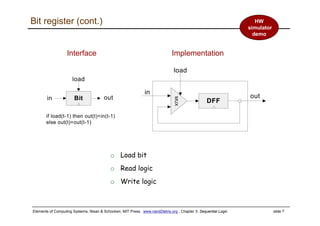


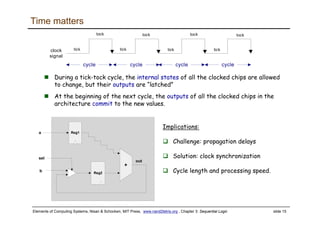


This document discusses sequential logic and how it differs from combinational logic. Sequential logic operates on both data and a clock signal, allowing it to store state information. It presents a hierarchy of memory elements starting with flip-flops, then binary cells, registers, RAM, and counters. Registers and RAM are built from arrays of flip-flops. Counters store and increment a value over time. All sequential chips use flip-flops and a clock to synchronize state changes.