Download as PDF, PPTX

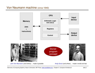
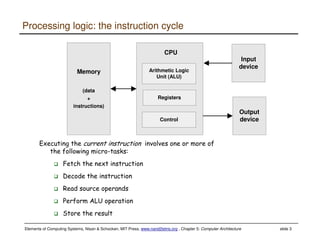
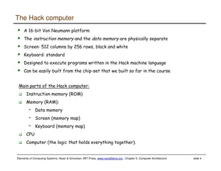
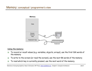
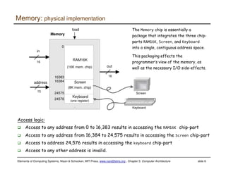
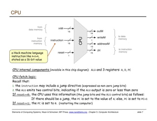
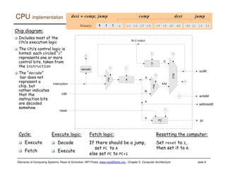

This document discusses the architecture of the Hack computer. It describes the main components of the Hack computer which are based on the Von Neumann architecture - the CPU, instruction memory, data memory, and input/output devices. The CPU fetches and executes instructions, accessing the separate instruction and data memories. The data memory also includes dedicated areas for the screen and keyboard. The chapter then discusses how these components are physically implemented on integrated chips to form the Hack computer. It also provides perspectives on how real computers evolved beyond this basic architecture.