Wearable 1.78 inch Square AMOLED Display 368*448 For Smart Watch Bracelet Screen On Cell Touch Panel Mipi Interface
•
0 likes•145 views

1.78 inch AMOLED is a low power consumption AMOLED with 368x448 resolution and MIPI/SPI interface. The IC mode is RM69090 which is widely used in wearable AMOLED displays such as 1.39" AMOLED. It has an integrated CTP with TMA525C touch IC. Application: Wearable, Medical equipment Whatsapp: +86 18566294218 Email: shawn.lee@panoxdisplay.com Skype: panoxshawn@outlook.com OLED/LCD supplier: www.panoxdisplay.com

Recommended
More Related Content
What's hot
What's hot (20)
Similar to Wearable 1.78 inch Square AMOLED Display 368*448 For Smart Watch Bracelet Screen On Cell Touch Panel Mipi Interface
Similar to Wearable 1.78 inch Square AMOLED Display 368*448 For Smart Watch Bracelet Screen On Cell Touch Panel Mipi Interface (20)
More from Shawn Lee
More from Shawn Lee (9)
Recently uploaded
Recently uploaded (20)
Wearable 1.78 inch Square AMOLED Display 368*448 For Smart Watch Bracelet Screen On Cell Touch Panel Mipi Interface
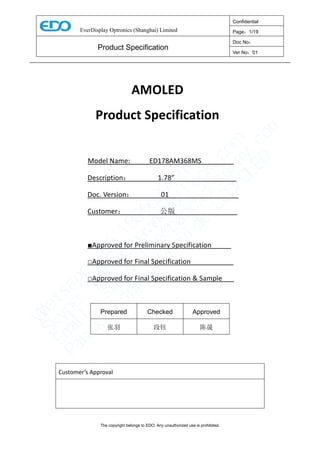
- 1. ED178AM368MS0 ED178AM368MS EverDisplay Optronics (Shanghai) Limited Confidential Page:1/19 Product Specification Doc No: Ver No:01 The copyright belongs to EDO, Any unauthorized use is prohibited. AMOLED Product Specification Model Name: ED178AM368MS Description: 1.78” Doc. Version: 01 Customer: 公版 ■Approved for Preliminary Specification □Approved for Final Specification □Approved for Final Specification & Sample Prepared Checked Approved 张羽 段钰 陈晟 Customer’s Approval W h a t s a p p : 8 6 1 8 5 6 6 2 9 4 2 1 8 S k y p e : p a n o x s h a w n @ o u t l o o k . c o m E m a i l : s h a w n . l e e @ p a n o x d i s p l a y . c o m P a n o x D i s p l a y P r o v i d e L C D / O L E D
- 2. EverDisplay Optronics (Shanghai) Limited Confidential Page:2/19 Product Specification Doc No: Ver No:01 The copyright belongs to EDO, Any unauthorized use is prohibited. Version History Version. No Date Contents Remark 01 2019-01-09 First Draft W h a t s a p p : 8 6 1 8 5 6 6 2 9 4 2 1 8 S k y p e : p a n o x s h a w n @ o u t l o o k . c o m E m a i l : s h a w n . l e e @ p a n o x d i s p l a y . c o m P a n o x D i s p l a y P r o v i d e L C D / O L E D
- 3. EverDisplay Optronics (Shanghai) Limited Confidential Page:3/19 Product Specification Doc No: Ver No:01 The copyright belongs to EDO, Any unauthorized use is prohibited. Contents 1 Scope.......................................................................................................................................................... 4 2 Features...................................................................................................................................................... 4 2.1 Product Applications ............................................................................................................................ 4 2.2 Product Features................................................................................................................................... 4 3 Mechanical Specifications ......................................................................................................................... 4 4 Maximum Rating ....................................................................................................................................... 4 5 Electrical Specifications............................................................................................................................. 5 5.1 Electrical Characteristics...................................................................................................................... 5 5.2 TP IC Recommended Operating Conditions ........................................................................................ 6 5.3 I/O Connection ..................................................................................................................................... 7 5.4 Graphic memory writing direction ....................................................................................................... 8 5.5 Recommended Operating Sequence..................................................................................................... 8 6 Electro-Optical Specification................................................................................................................... 12 7 Reliability................................................................................................................................................. 17 7.1 Environmental Test............................................................................................................................. 17 7.2 Electrical Test ..................................................................................................................................... 17 7.3 Mechanical Test.................................................................................................................................. 17 8 Outline Dimension Drawing.................................................................................................................... 18 9 Packing Specification................................................................................................................................ 19 10 The Control of Hazardous Substances...................................................................................................... 19 W h a t s a p p : 8 6 1 8 5 6 6 2 9 4 2 1 8 S k y p e : p a n o x s h a w n @ o u t l o o k . c o m E m a i l : s h a w n . l e e @ p a n o x d i s p l a y . c o m P a n o x D i s p l a y P r o v i d e L C D / O L E D
- 4. EverDisplay Optronics (Shanghai) Limited Confidential Page:4/19 Product Specification Doc No: Ver No:01 The copyright belongs to EDO, Any unauthorized use is prohibited. 1 Scope This Specification defines AMOLED manufactured by EverDisplay Optronics(Shanghai) Limited, from here on refer as EDO. In the case of any unspecified item, it may require both EDO and the party designs this module into its product to work out a solution. 2 Features 2.1 Product Applications Smart Watch 2.2 Product Features 1) Display color:16.7M (RGB x 8bits) 2) Display format:1.78”(368RGBx448) 3) Pixel arrangement:Real RGB arrangement 4) Interface:MIPI/SPI 3 Mechanical Specifications Item Specification unit LTPS Glass outline 30.6*37.99 mm Encapsulation Glass outline 30.6*37.24 mm Number of dots 368(W) x RGB x 448(H) dots Active area 28.7*34.94 mm Diagonal size 1.78 inch Pixel pitch 78*78 μm Glass thickness (LTPS/Encap. glass) 0.2 / 0.3 mm Weight TBD g 4 Maximum Rating Parameter Symbol Spec Unit Note Min. Typ. Max. Analog/boost power voltage VCI -0.3 - 5.5 V - I/O voltage VDDIO -0.3 - 5.5 V - Operating temperature Top -20 - 70 ℃ - Storage temperature Tstg -40 - 80 ℃ - W h a t s a p p : 8 6 1 8 5 6 6 2 9 4 2 1 8 S k y p e : p a n o x s h a w n @ o u t l o o k . c o m E m a i l : s h a w n . l e e @ p a n o x d i s p l a y . c o m P a n o x D i s p l a y P r o v i d e L C D / O L E D
- 5. EverDisplay Optronics (Shanghai) Limited Confidential Page:5/19 Product Specification Doc No: Ver No:01 The copyright belongs to EDO, Any unauthorized use is prohibited. 5 Electrical Specifications 5.1 Electrical Characteristics Power Characteristic: Item Symbol Min. Typ. Max. Unit Remark Battery power Voltage Vbat 2.9 3.7 4.8 V - Digital Power supply VDDIO 1.65 1.8 1.95 V Ref 1) Normal Mode Power Supply: VDDIO=1.8V Vbat=3.7V Frame Frequency: Fframe =60HZ @ 25degC, Brightness 350 nits, Command Mode, Display Condition Symbol Min. Typ. Max. Unit Remark 100% Pixel On,350nits Normal mode - 186 210 mW Ref 2) Idle Mode Power Supply: VDDIO=1.8V Vbat=3.7V Frame Frequency: Fframe =15HZ @ 25degC, Brightness 30 nits, Display Condition Symbol Min. Typ. Max. Unit Remark 10% Pixel On,30nits Idle mode - 12 16 mW Ref 3) Deep Standby Mode Display Condition Symbol Min. Typ. Max. Unit Remark All Pixel Off,0nits/ Vci off/Vddio on Standby mode - - 50 μW - 5.1.2 Driver IC RM69090 (refer to the datasheet). W h a t s a p p : 8 6 1 8 5 6 6 2 9 4 2 1 8 S k y p e : p a n o x s h a w n @ o u t l o o k . c o m E m a i l : s h a w n . l e e @ p a n o x d i s p l a y . c o m P a n o x D i s p l a y P r o v i d e L C D / O L E D
- 6. EverDisplay Optronics (Shanghai) Limited Confidential Page:6/19 Product Specification Doc No: Ver No:01 The copyright belongs to EDO, Any unauthorized use is prohibited. 5.2 TP IC Recommended Operating Conditions Touch IC: TMA525C (refer to the datasheet) Symbol Description Min TYP MAX UNIT VCCA Analog power supply voltage 2.7 2.8 3.6 V VIN(I2C) Input voltage range 0 - 3.6 V VOUT(I2C) Output voltage range 0 - 3.6 V VIN(INT) Input voltage range 0 - 3.6 V VOUT(INT) Output voltage range 0 - 3.6 V VOUT(TX) Output voltage range 0 - VCCA V VOUT(RX) Input voltage range 0 - VCCA V W h a t s a p p : 8 6 1 8 5 6 6 2 9 4 2 1 8 S k y p e : p a n o x s h a w n @ o u t l o o k . c o m E m a i l : s h a w n . l e e @ p a n o x d i s p l a y . c o m P a n o x D i s p l a y P r o v i d e L C D / O L E D
- 7. EverDisplay Optronics (Shanghai) Limited Confidential Page:7/19 Product Specification Doc No: Ver No:01 The copyright belongs to EDO, Any unauthorized use is prohibited. Item Spec Remark Operating voltage 2.7-3.6V Operating current 2mA Linearity Center part≤1mm Test tool:φ7mm copper cylinder The peripheral position ≤2mm Sensitivity No broken line Lineation with 5mm/s&20mm/s respectively by Φ7mm copper cylinder Response time ≤10ms 5.3 I/O Connection(TBD) # Pin name I/O Description 1 2 3 4 5 6 7 8 9 10 11 12 13 14 15 16 17 18 19 W h a t s a p p : 8 6 1 8 5 6 6 2 9 4 2 1 8 S k y p e : p a n o x s h a w n @ o u t l o o k . c o m E m a i l : s h a w n . l e e @ p a n o x d i s p l a y . c o m P a n o x D i s p l a y P r o v i d e L C D / O L E D
- 8. EverDisplay Optronics (Shanghai) Limited Confidential Page:8/19 Product Specification Doc No: Ver No:01 The copyright belongs to EDO, Any unauthorized use is prohibited. 20 21 22 23 24 5.4 Graphic memory writing direction 5.5 Recommended Operating Sequence 5.5.1 Power on sequence W h a t s a p p : 8 6 1 8 5 6 6 2 9 4 2 1 8 S k y p e : p a n o x s h a w n @ o u t l o o k . c o m E m a i l : s h a w n . l e e @ p a n o x d i s p l a y . c o m P a n o x D i s p l a y P r o v i d e L C D / O L E D
- 9. EverDisplay Optronics (Shanghai) Limited Confidential Page:9/19 Product Specification Doc No: Ver No:01 The copyright belongs to EDO, Any unauthorized use is prohibited. 5.5.2 Power off sequence 5.5.3 AC Characteristics(MIPI) HS Data Transmission Burst HS Clock Transmission W h a t s a p p : 8 6 1 8 5 6 6 2 9 4 2 1 8 S k y p e : p a n o x s h a w n @ o u t l o o k . c o m E m a i l : s h a w n . l e e @ p a n o x d i s p l a y . c o m P a n o x D i s p l a y P r o v i d e L C D / O L E D
- 10. EverDisplay Optronics (Shanghai) Limited Confidential Page:10/19 Product Specification Doc No: Ver No:01 The copyright belongs to EDO, Any unauthorized use is prohibited. Turnaround Procedure Timing Parameters Symbol Description Min Typ Max Unit TREOT 30%-85% rise time and fall time - - 35 ns TCLK-MISS Timeout for receiver to detect absence of Clock transitions and disable the Clock Lane HS-RX. - - 60 ns TCLK-POST*1 Time that the transmitter continues to send HS clock after the last associated Data Lane has transitioned to LP Mode. Interval is defined as the period from the end of THS-TRAIL to the beginning of TCLK-TRAIL. 60ns + 52*UI (For DCS) - - ns TCLK-PRE Time that the HS clock shall be driven by the transmitter prior to any 8 - - ns W h a t s a p p : 8 6 1 8 5 6 6 2 9 4 2 1 8 S k y p e : p a n o x s h a w n @ o u t l o o k . c o m E m a i l : s h a w n . l e e @ p a n o x d i s p l a y . c o m P a n o x D i s p l a y P r o v i d e L C D / O L E D
- 11. EverDisplay Optronics (Shanghai) Limited Confidential Page:11/19 Product Specification Doc No: Ver No:01 The copyright belongs to EDO, Any unauthorized use is prohibited. associated Data Lane beginning the transition from LP to HS mode. TCLK-SETTLE Time interval during which the HS receiver shall ignore any Clock Lane HS transitions, starting from the beginning of TCLK-PRE. 95 - 300 ns TCLK-TERM-EN Time for the Clock Lane receiver to enable the HS line termination,starting from the time point when Dn crosses VIL,MAX. Time for Dn to reach VTERM-EN 38 ns THS-SETTLE Time interval during which the HS receiver shall ignore any Data Lane HS transitions, starting from the beginning of THSPREPARE. 85 ns + 6*UI 145 ns + 10*UI ns TEOT Time from start of THS-TRAIL or TCLK-TRAIL period to start of LP-11 state - - 105ns+48*UI ns THS-EXIT(1) time to drive LP-11 after HS burst 100 - - ns THS-PREPARE Time to drive LP-00 to prepare for HS transmission 40ns + 4*UI - 85ns+6*UI ns THS-PREPARE + THS-ZERO THS-PREPARE + Time to drive HS-0 before the Sync sequence 145ns + 10*UI - - ns THS-SKIP Time-out at RX to ignore transition period of EoT 40 - 55ns+4*UI ns THS-TRAIL Time to drive flipped differential state after last payload data bit of a HS transmission burst 60 + 4*UI - - ns TLPX Length of any Low-Power state period 50 - - ns Ratio TLPX Ratio of TLPX(MASTER)/TLPS(SLAVE) 2/3 - 3/2 ns W h a t s a p p : 8 6 1 8 5 6 6 2 9 4 2 1 8 S k y p e : p a n o x s h a w n @ o u t l o o k . c o m E m a i l : s h a w n . l e e @ p a n o x d i s p l a y . c o m P a n o x D i s p l a y P r o v i d e L C D / O L E D
- 12. EverDisplay Optronics (Shanghai) Limited Confidential Page:12/19 Product Specification Doc No: Ver No:01 The copyright belongs to EDO, Any unauthorized use is prohibited. between Master and Slave side TTA-GET Time to drive LP-00 by new TX 5*TLPX 5*TLPX 5*TLPX ns TTA-GO Time to drive LP-00 after Turnaround Request 4*TLPX 4*TLPX 4*TLPX ns TTA-SURE Time-out before new TX side starts driving TLPX - 2*TLPX ns Timing requirements for RESETB When RESETB of the reset pin equals to Low, it will be in the condition of reset. When it is in the condition of reset, it will make the device recover the initial set. However, in order to avoid the reset noise cause reset, there is a mechanism to judge about whether the reset is needed or not. The closed interval of Low can be shown as the following. (Test condition: VDDIO=1.65V~3.6V, VSS=0V, TA=-20℃~+70℃) Parameter Symbol Conditions Spec Unit Min. Typ. Max. Reset low pulse width Trst - 20 - - µs Table: Reset timing Trst 20% 20% RESETB 6 Electro-Optical Specification Test condition:25℃±3℃,65±20%RH,darkroom。 No Item Symbol Condition Value Unit Remar k Min. Typ. Max. 1 Brightness L Full white Without CG 315 350 385 cd/m2 Note1. 2 Brightness Uniformity UL Full white 80 85 - % Note4 3 Contrast Ratio CR Normal Θ=Φ=0° 10000 100000 - - Note3. 4 Response time Ton+Toff Normal Θ=Φ=0° - 2 4 ms Note2. W h a t s a p p : 8 6 1 8 5 6 6 2 9 4 2 1 8 S k y p e : p a n o x s h a w n @ o u t l o o k . c o m E m a i l : s h a w n . l e e @ p a n o x d i s p l a y . c o m P a n o x D i s p l a y P r o v i d e L C D / O L E D
- 13. EverDisplay Optronics (Shanghai) Limited Confidential Page:13/19 Product Specification Doc No: Ver No:01 The copyright belongs to EDO, Any unauthorized use is prohibited. 5 Color Coordinate of CIE1931 White X Normal Θ=Φ=0° 0.28 0.30 0.32 - Note1. Y 0.29 0.31 0.33 Red X 0.648 0.688 0.728 Y 0.272 0.312 0.352 Green X 0.17 0.22 0.27 Y 0.675 0.735 0.785 Blue X 0.102 0.142 0.182 Y 0.002 0.042 0.082 6 Color Gamut NTSC CIE1931 90 105 - % 7 Viewing Angle Top/Botton/Righ t/Left CR ratio ≥1000 80 ° Note3. 8 Gamma Log(Lv- Lb)=log(V)+log(a ) V(Gray)= 48,72,104,132, 164,192,224 Lum(gray255)=3 50nit 2.0 2.2 2.4 - 9 Flicker Normal Θ=Φ=0° - -35 -30 dB Note6. 10 Crosstalk - - - 4 % Note7. 11 Color shift θL=30° 5 5.5 12 OLED Life Time 0.95*(TYP brightness) At 25℃,with white color pattern 240 hrs Note8. 13 Image Retention With 8*8 black-white chess board test image, lighting on with maximum luminance for 10min 8*8 black-white chess board 10min,to G128,20s disappear W h a t s a p p : 8 6 1 8 5 6 6 2 9 4 2 1 8 S k y p e : p a n o x s h a w n @ o u t l o o k . c o m E m a i l : s h a w n . l e e @ p a n o x d i s p l a y . c o m P a n o x D i s p l a y P r o v i d e L C D / O L E D
- 14. EverDisplay Optronics (Shanghai) Limited Confidential Page:14/19 Product Specification Doc No: Ver No:01 The copyright belongs to EDO, Any unauthorized use is prohibited. See the note in the table below: No Item Details Note1 Brightne ss Note 2 Respons e time Note 3 Viewing Angle Contrast Ratio Dark Room C.R=LW/LB LW: full white brightness of display center P0; LB: full black brightness of display center P0. Note 4 Brightne ss Uniformi ty W h a t s a p p : 8 6 1 8 5 6 6 2 9 4 2 1 8 S k y p e : p a n o x s h a w n @ o u t l o o k . c o m E m a i l : s h a w n . l e e @ p a n o x d i s p l a y . c o m P a n o x D i s p l a y P r o v i d e L C D / O L E D
- 15. EverDisplay Optronics (Shanghai) Limited Confidential Page:15/19 Product Specification Doc No: Ver No:01 The copyright belongs to EDO, Any unauthorized use is prohibited. Note 5 Luminan ce decrease ration Definition of Luminance decrease ratio Test pattern : Full White The luminance decrease ratio is calculated by using following formula: Note 6 Flicker Suggested Instruments: Konica Minolta CA-310 or Klein Instruments K-8 The flicker level is defined by Fast Fourier Transformation (FTT) as follows: Where fFFTC(n) is the n-th FFT coefficient. fFFTC(0) is the 0-th FFT coefficient which is DC component. FS(Hz) is the flicker sensitivity as a function of frequency. The peak flicker level shall be reported based on the calculation using above formula in which FS(Hz) is determined by the flicker weighing factor shown below. W h a t s a p p : 8 6 1 8 5 6 6 2 9 4 2 1 8 S k y p e : p a n o x s h a w n @ o u t l o o k . c o m E m a i l : s h a w n . l e e @ p a n o x d i s p l a y . c o m P a n o x D i s p l a y P r o v i d e L C D / O L E D
- 16. EverDisplay Optronics (Shanghai) Limited Confidential Page:16/19 Product Specification Doc No: Ver No:01 The copyright belongs to EDO, Any unauthorized use is prohibited. Note 7 Crosstal k Crosstalk shall be calculated by the luminance of B1~B4 and G1~G4 in the patterns shown below. Box Pattern: L128 gray level background with a L255 White window in the central area. Gray Pattern: L128 gray level background only. Note 8 Life Time OLED life time is defined by the Minimum Duration Time that the luminance is decayed to a specific ratio (ex. 92%) of initial state. Test Pattern under duration period: L255 White W h a t s a p p : 8 6 1 8 5 6 6 2 9 4 2 1 8 S k y p e : p a n o x s h a w n @ o u t l o o k . c o m E m a i l : s h a w n . l e e @ p a n o x d i s p l a y . c o m P a n o x D i s p l a y P r o v i d e L C D / O L E D
- 17. EverDisplay Optronics (Shanghai) Limited Confidential Page:17/19 Product Specification Doc No: Ver No:01 The copyright belongs to EDO, Any unauthorized use is prohibited. 7 Reliability 7.1 Environmental Test Item Main spec No. of failures / No. of examinations High Temperature Operation 70℃/ 128hrs 0/10 Low Temperature Operation -20℃/ 128hrs 0/10 High Temperature Storage 80℃/ 128hrs 0/10 Low Temperature Storage -40℃/ 128hrs 0/10 High Temperature Humidity Operation 60℃/93%RH/ 128hrs 0/32 Thermal Shock -40℃~85℃ dwell time=0.5hr, 50cycles. 0/10 7.2 Electrical Test Item Main spec Note Air Discharge ±4 kV , 150pF/330Ω (Module level; without CG) 5Points, Each 10times. After one time discharge, panel and gun touch the ground, through the whole test, turn on ion fan. No degradation of OLED performance after this test. Contact Discharge ±2kV, 150pF/330Ω (Module level; without CG) 7.3 Mechanical Test Test item Test condition Note Packing vibration-proof test 2g, f=10->55->10Hz apply in each of X, Y, and Z direction for 30 min Package Packing Drop test Drop the packing from 60cm height, 6-faces, 3-edges and 1-corner(one time for each) Package W h a t s a p p : 8 6 1 8 5 6 6 2 9 4 2 1 8 S k y p e : p a n o x s h a w n @ o u t l o o k . c o m E m a i l : s h a w n . l e e @ p a n o x d i s p l a y . c o m P a n o x D i s p l a y P r o v i d e L C D / O L E D
- 18. EverDisplay Optronics (Shanghai) Limited Confidential Page:18/19 Product Specification Doc No: Ver No:01 The copyright belongs to EDO, Any unauthorized use is prohibited. 8 Outline Dimension Drawing W h a t s a p p : 8 6 1 8 5 6 6 2 9 4 2 1 8 S k y p e : p a n o x s h a w n @ o u t l o o k . c o m E m a i l : s h a w n . l e e @ p a n o x d i s p l a y . c o m P a n o x D i s p l a y P r o v i d e L C D / O L E D
- 19. EverDisplay Optronics (Shanghai) Limited Confidential Page:19/19 Product Specification Doc No: Ver No:01 The copyright belongs to EDO, Any unauthorized use is prohibited. 9 Packing Specification TBD 10 The Control of Hazardous Substances The control of Hazardous substances refer to EDO document 《有害物质管控标准书》 (Standard document for the Control of Hazardous substances) EDO –IS- 110, the latest version. W h a t s a p p : 8 6 1 8 5 6 6 2 9 4 2 1 8 S k y p e : p a n o x s h a w n @ o u t l o o k . c o m E m a i l : s h a w n . l e e @ p a n o x d i s p l a y . c o m P a n o x D i s p l a y P r o v i d e L C D / O L E D