5.5 inch Amoled (1080x1920) Datasheet
•
0 likes•469 views

Display Type: AMOLED Display Brand: AUO Interface: MIPI Screen Size: 5.5 Orientation: Portrait Display Color: Full Color Resolution: 1080(RGB)×1920 Driver IC: COGBuilt-in RM69070 Active Area(mm): 68.04(W)×120.96(H) ×0.88(D)mm Luminance: 350 cd/m² (Typ.) Viewing Angle: 80/80/80/80 (Min.)(CR≥1600) Color Depth: 16.7M 103% (CIE1931) Signal Type: MIPI (2 data lanes), 40 pins, Connector Voltage Supply: 1.8/3.0/4.6/7.6V (Typ.)(IOVCC/VCI/OVDD/AVDD) Operating Temp: -40 ~ 85 °C ............... More about 5" AMOLED: https://www.panoxdisplay.com/html/products/amoled-57-1.html

Recommended
More Related Content
What's hot
What's hot (20)
Similar to 5.5 inch Amoled (1080x1920) Datasheet
Similar to 5.5 inch Amoled (1080x1920) Datasheet (20)
Recently uploaded
Recently uploaded (20)
5.5 inch Amoled (1080x1920) Datasheet
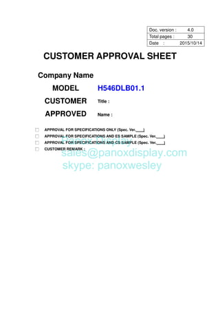
- 1. CUSTOMER APPROVAL SHEET Company Name MODEL H546DLB01.1 CUSTOMER APPROVED Title : Name : □ APPROVAL FOR SPECIFICATIONS ONLY (Spec. Ver. ) □ APPROVAL FOR SPECIFICATIONS AND ES SAMPLE (Spec. Ver. ) □ APPROVAL FOR SPECIFICATIONS AND CS SAMPLE (Spec. Ver. ) □ CUSTOMER REMARK : Doc. version : 4.0 Total pages : 30 Date : 2015/10/14 Panox Display sales@panoxdisplay.com skype: panoxwesley
- 2. 1 Product Specification 5.46" COLOR AMOLED MODULE MODEL NAME: H546DLB01.1 Trial-run sample P/N: 95.05H33.100 MP product P/N: (TBD) < ◆ >Preliminary Specification < >Final Specification Panox Display sales@panoxdisplay.com skype: panoxwesley
- 3. 2 Record of Revision Version Revise Date Page Content 1.0 2015-04-28 1~31 First Draft 2.0 2015-04-30 26 Carton Test (Vibration) Criteria Modified 3.0 2015-06-02 18 Power On Sequence Diagram Modified 4.0 2015-07-31 9 22 24 Display Current Consumption Optical Specification Uniformity condition Panox Display sales@panoxdisplay.com skype: panoxwesley
- 4. 3 Contents A. General Specification ..................................................................................................................................4 1. Physical Specifications ......................................................................................................................4 2. Pin Assignment ...................................................................................................................................5 3. Absolute Maximum Ratings ...............................................................................................................6 B. DC Characteristics.......................................................................................................................................7 1. Typical Operating Conditions ............................................................................................................7 2. Display Current Consumption ...........................................................................................................8 3. Touch Panel Current Consumption...................................................................................................8 4. Recommend DC/DC Power IC Application Circuit...........................................................................9 C. AC Characteristics.....................................................................................................................................10 1. Display Video Timing ........................................................................................................................10 2. MIPI Interface Characteristics..........................................................................................................11 3. Display RESET Timing Characteristics...........................................................................................14 4. Touch Panel I2C Timing Characteristics.........................................................................................15 5. Touch Panel RESET Timing Characteristics ..................................................................................16 6. Recommended Operating Sequence ..............................................................................................16 D. Touch Specifications .................................................................................................................................20 E. Optical Specification..................................................................................................................................21 F. Reliability Test Items..................................................................................................................................25 G. Precautions.................................................................................................................................................27 H. Packing Information...................................................................................................................................28 I. Outline Dimension .....................................................................................................................................29 Panox Display sales@panoxdisplay.com skype: panoxwesley
- 5. 4 A. General Specification 1. Physical Specifications NO Item unit Specification Remark 1 Screen Size inch 5.46” Diagonal 2 Display Resolution -- 1080(H) X 1920(V) Full HD 3 Outline Dimension mm 70.84 (H) × 128.01(V) × 0.877(T) 4 Active Area mm 68.04 (H)×120.96(V) 5 Pixel Pitch um 63 6 Color Configuration -- R, G, B 7 Color Depth -- 16.7M 8-bit x RGB 8 NTSC Ratio % ~ 100 9 Display Mode -- AMOLED 10 Panel Surface Treatment -- Hard Coat (3H) 11 Interface -- MIPI DSI – Video Mode 12 Driver IC RM69071 13 Touch IC S3508 14 Multi-finger Touch 10 Panox Display sales@panoxdisplay.com skype: panoxwesley
- 6. 5 2. Pin Assignment AMOLED Main FPC Pin assignment # Pin_name I/O/P Description 1 OVSS P OLED Power 2 OVDD P OLED Power 3 OVSS P OLED Power 4 OVDD P OLED Power 5 OVSS P OLED Power 6 OVDD P OLED Power 7 NC - Leave this pin OPEN 8 NC - Leave this pin OPEN 9 GND P Ground 10 AVDD P Display Driver IC Source Analog Power 11 D2P I MIPI DSI data 12 TP_VCC P Touch panel analog I/O power supply 13 D2N I MIPI DSI data 14 TP_VDDI P Touch Panel I/O voltage power supply 15 GND P Ground 16 TP_SDA I/O Touch panel I2C data 17 D1P I MIPI DSI data 18 TP_SCL I/O Touch panel I2C clock 19 D1N I MIPI DSI data 20 TP_RESX I Touch panel reset 21 GND P Ground 22 TP_INT O Touch panel interrupt output 23 CKP I MIPI DSI data 24 NC - Leave this pin OPEN 25 CKN I MIPI DSI data 26 NC - Leave this pin OPEN 27 GND P Ground 28 VCI P Display Driver Analog IC Power Panox Display sales@panoxdisplay.com skype: panoxwesley
- 7. 6 29 D0P I/O MIPI DSI data 30 IOVCC P Display Driver Digital IC Power 31 D0N I/O MIPI DSI data 32 RESX I This signal will reset the device and must be applied to properly initialize the chip. Signal is active low. 33 GND P Ground 34 AVDD_EN O DC/DC power IC control signal, please connect to power IC EN pin 35 D3P I MIPI DSI data 36 SWIRE O DC/DC power IC control signal, please connect to power IC CTRL pin 37 D3N I MIPI DSI data 38 MTP_Power P Leave this pin OPEN 39 GND P Ground 40 GND P Ground Recommended connector: JAE WP7B-S040VA1 3. Absolute Maximum Ratings Item Symbol Min. Max. Unit Remark OLED Power supply OVDD - 4.6 V OLED Power supply OVSS - -2.9 V Driver IC Source output power supply AVDD - 7.6 V Digital Power supply IOVCC -0.3 +1.95 V Analog Power supply VCI -0.3 +3.2 V Touch analog power supply TP_VCC -0.3 +4.0 V Touch digital power supply TP_VDDI -0.3 +2.0 V Operating temperature (Ambient) Topr -40 +85 ℃ Storage temperature (Ambient) Tstg -55 +125 ℃ Note : If the module exceeds the absolute maximum ratings, it may be damaged permanently. Also, if the module operates with the absolute maximum ratings for a long time, the reliability may drop. Panox Display sales@panoxdisplay.com skype: panoxwesley
- 8. 7 B. DC Characteristics 1. Typical Operating Conditions Item Symbol Min. Typ. Max. Unit Remark OLED Power supply OVDD - 4.6 - V OLED Power supply OVSS - -2.9 - V Driver IC Source output power supply AVDD - 7.6 - V Digital Power supply IOVCC 1.65 1.8 1.95 V Analog Power supply VCI 2.8 3 3.2 V Touch analog power supply TP_VCC 2.70 3.10 3.60 V Touch digital power supply TP_VDDI 1.65 1.80 1.95 V H Level VIH 0.8* IOVCC - IOVCC V Input Signal Voltage L Level VIL 0 - 0.2* IOVCC V RESX Note 1: The operation is guaranteed under the recommended operating conditions only. The operation is not guaranteed if a quick voltage change occurs during the operation. To prevent the noise, a bypass capacitor must be inserted into the line closed to the power pin. Panox Display sales@panoxdisplay.com skype: panoxwesley
- 9. 8 2. Display Current Consumption Mode Symbol Condition Min. Typ. Max. Unit Remark IAVDD - 15 30 mA IVCI - 3 3 mA IIOVCC - 38 40 mA Note 1 IOVDD - 190 200 mA Normal IOVSS - 190 200 mA Note 2 IAVDD - 0.2 1 uA IVCI - 2 3 mA IIOVCC - 25 30 uA IOVDD - 0 0 uA Deep Standby (DSTB=1) IOVSS AVDD = 7.6V VCI = 3V IOVCC = 1.8V OVDD = 4.6V OVSS = -2.9V 25℃ - 0 0 uA Note 1: Typ. Max. Note 2: 350 nits White. 3. Touch Panel Current Consumption Mode Symbol Condition Min Typ. Max Unit ITP_VDDI - 18 20 mA Active (1finger) ITP_VCC - 12 14 mA ITP_VDDI - 25 28 mA Active (10fingers) ITP_VCC - 12 14 mA ITP_VDDI - 0.4 0.5 mA Normal Operation ITP_VCC - 0.4 0.5 mA ITP_VDDI - 7 8 µASensor Sleep (Deep sleep) ITP_VCC TP_VDDI = 1.8V TP_VCC=3.1V Report Rate: 100Hz Doze Interval: 30 ms (28Rx X 16Tx) - 6 7 µA Panox Display sales@panoxdisplay.com skype: panoxwesley
- 10. 9 4. Recommend DC/DC Power IC Application Circuit Vendor Model TI TPS65632RTER Richtek RT4720A Bill of MaterialsPanox Display sales@panoxdisplay.com skype: panoxwesley
- 11. 10 C. AC Characteristics 1. Display Video Timing Active Area 5 11 1080 32 57192012 Back Porch HSync Active Area Front PorchVSync BackPorch FrontPorchActiveArea Panox Display sales@panoxdisplay.com skype: panoxwesley
- 12. 11 2. MIPI Interface Characteristics HS Data Transmission Burst HS clock transmission VIH(min) VIL(max) VIH(min) VIL(max) Data Lane Dp/Dn Clock Lane CLKp/CLKn TCLK-POST TCLK-TERM-EN TCLK-PREPARE TCLK-ZERO TCLK-PRETLPXTHS-EXITTCLK-TRAIL Disconnect Terminator Disconnect Terminator TLPX THS-PREPARE TD-TERM-EN Turnaround Procedure Panox Display sales@panoxdisplay.com skype: panoxwesley
- 13. 12 Timing Parameters Symbol Description Min Typ Max Unit TCLK-POST Time that the transmitter continues to send HS clock after the last associated Data Lane has transitioned to LP Mode. Interval is defined as the period from the end of THS- TRAIL to the beginning of TCLK-TRAIL . 60ns + 52*UI ns TCLK-TRAIL Time that the transmitter drives the HS-0 state after the last payload clock bit of a HS transmission burst. 60 ns THS-EXIT Time that the transmitter drives LP-11 following a HS burst. 300 ns TCLK-TERM-EN Time for the Clock Lane receiver to enable the HS line termination, starting from the time point when Dn crosses VIL,MAX . Time for Dn to reach VTERM-EN 38 ns TCLK-PREPARE Time that the transmitter drives the Clock Lane LP-00 Line state immediately before the HS-0 Line state starting the HS transmission. 38 95 ns TCLK-PRE Time that the HS clock shall be driven by the transmitter prior to any associated Data Lane beginning the transition from LP to HS mode. 8 UI TCLK-PREPARE + TCLK-ZERO TCLK-PREPARE + time that the transmitter drives the HS-0 state prior to starting the Clock. 300 ns TD-TERM-EN Time for the Data Lane receiver to enable the HS line termination, starting from the time point when Dn crosses VIL,MAX . Time for Dn to reach VTERM-EN 35ns +4*UI THS-PREPARE Time that the transmitter drives the Data Lane LP-00 Line state immediately before the HS-0 Line state starting the HS transmission 40ns + 4*UI 85 ns + 6*UI ns THS-PREPARE + THS-ZERO THS-PREPARE + time that the transmitter drives the HS-0 state prior to transmitting the Sync sequence. 145ns + 10*UI ns THS-TRAIL Time that the transmitter drives the flipped differential state after last payload data bit of a HS transmission burst 60ns + 4*UI ns Panox Display sales@panoxdisplay.com skype: panoxwesley
- 14. 13 TLPX(M) Transmitted length of any Low-Power state period of MCU to display module 50 150 ns TTA-SURE(M) Time that the display module waits after the LP-10 state before transmitting the Bridge state (LP-00) during a Link Turnaround. TLPX(M) 2*TLPX(M) ns TLPX(D) Transmitted length of any Low-Power state period of display module to MCU 50 150 ns TTA-GET(D) Time that the display module drives the Bridge state (LP-00) after accepting control during a Link Turnaround. 5*TLPX(D) ns TTA-GO(D) Time that the display module drives the Bridge state (LP-00) before releasing control during a Link Turnaround. 4*TLPX(D) ns TTA-SURE(D) Time that the MPU waits after the LP-10 state before transmitting the Bridge state (LP-00) during a Link Turnaround. TLPX(D) 2*TLPX(D) ns Panox Display sales@panoxdisplay.com skype: panoxwesley
- 15. 14 3. Display RESET Timing Characteristics Reset input timing IOVCC=1.65 to 1.95V, VCI=2.8 to 3.2V, GND=0V, Ta=-40 to 85℃ Timing Parameters Symbol Parameter Related Pins MIN TYP MAX Note Unit tRESW *1) Reset low pulse width RESX 10 - - - µs - - - 5 When reset applied during Sleep in mode ms tREST *2) Reset complete time - - 120 When reset applied during Sleep out mode ms Note 1. Spike due to an electrostatic discharge on RESX line does not cause irregular system reset according to the table below. RESX Pulse Action Shorter than 5µs Invalid Reset Longer than 10µs Valid Reset Between 5µs and 10µs Reset Initialization Precedure Note 2. During the resetting period, the display will be blanked (The display is entering blanking sequence, which maximum time is 120 ms, when Reset Starts in Sleep Out –mode. The display remains the blank state in Sleep In –mode) and then return to Default condition for H/W reset. Note 3. During Reset Complete Time, data in OTP will be latched to internal register during this period. This loading is done every time when there is H/W reset complete time (tREST) within 5ms after a rising edge of RESX. Note 4. Spike Rejection also applies during a valid reset pulse as shown below: Note 5. It is necessary to wait 5msec after releasing RESX before sending commands. Also Sleep Out command cannot be sent for 120msec. Panox Display sales@panoxdisplay.com skype: panoxwesley
- 16. 15 4. Touch Panel I2C Timing Characteristics I2C address: 0x20 I2C timing Timing Parameters Standard- Mode Host Fast-Mode Host Symbol Parameter Min. Max. Min. Max. Unit fSCL TP_SCL clock frequency - 100 - 400 kHz Tcstr Stretch time - 25 - 25 µs Thd;sta Hold time (repeated) START condition. After this period, the first clock pulse is generated. 4.0 - 0.6 - µs Tlow LOW period of the TP_SCL clock 4.7 - 1.3 - µs Thigh HIGH period of the TP_SCL clock 4.0 - 0.6 - µs Tsu;sta Set-up time for a repeated START condition 4.7 - 0.6 - µs Thd;dat Data hold time 0 3.45 0 0.9 µs Thd;dato Data out hold time - 0 - 0 µs Tsu;dat Data set-up time 250 - 100 - ns Tr Rise time of both TP_SDA and TP_SCL signals - 1000 20 + 0.1 Cb 300 ns Tf Fall time of both TP_SDA and TP_SCL signals - 300 20 + 0.1 Cb 300 ns Tsu:sto Set-up time for STOP condition 4.0 - 0.6 - µs tBUF Bus free time between a STOP and START condition 4.7 - 1.3 - µs Cb Capacitive load for each bus line - 400 - 400 pF VnL Noise margin at the LOW level for each connected device (including hysteresis) 0.1 TP_VDDI 0.1 TP_VDDI V VnH Noise margin at the HIGH level for each connected device (including hysteresis) 0.2 TP_VDDI - 0.2 TP_VDDI - V TP_SDA TP_SCL TP_SCL TP_SDA Panox Display sales@panoxdisplay.com skype: panoxwesley
- 17. 16 5. Touch Panel RESET Timing Characteristics Reset input timing Timing Parameters Symbol Min. Max. Unit Treset (TP_RESX) 100 - ns Tbl_start - 2 ms Tbl_active - 11 ms Treboot - 16 ms 6. Recommended Operating Sequence State Diagram TP_RESX TP_INT Panox Display sales@panoxdisplay.com skype: panoxwesley
- 18. 17 Power Structure Power on sequence Power off sequence VCI IOVCC RESX MiPi DSI AVDD EN AVDD OVDD OVSS Control By Customer Control By Display Driver IC Control By DC/DC Power IC Display Off Sleep In 16.6 ms 16.6 ms > 10ms > 10 ms > 166 ms SWIRE Panox Display sales@panoxdisplay.com skype: panoxwesley
- 19. 18 Initial Setting: Item Parameter Quantity Address P0 1 1 0xFE 0x08 2 1 0x03 0x40 3 1 0x07 0x1A 4 1 0xFE 0x00 5 1 0x51 0xFF Sleep Out: Item Parameter Quantity Address P0 1 1 0x11 0x00 Display On: Item Parameter Quantity Address P0 1 1 0x29 0x00 Sleep In Item Parameter Quantity Address P0 1 1 0x10 0x00 Display Off: Item Parameter Quantity Address P0 1 1 0x28 0x00 Panox Display sales@panoxdisplay.com skype: panoxwesley
- 20. 19 Touch Panel Power on Sequence Symbol Min. Max. Unit Tattn_en 5 21 ms Tpowerup - 60 ms Tbl_start (bootloader start) - 46 ms Tbl_active (bootloader active) - 11 ms TP_SDA TP_SCL TP_INT TP_INT TP_VCC TP_VDDI Panox Display sales@panoxdisplay.com skype: panoxwesley
- 21. 20 D. Touch Specifications No. Item Spec. Remark 1 Touch IC S3508 Synaptics 2 Multi-Finger 10 3 Report Rate ≧ 100Hz Accuracy. ≦2.0mm 4 Performance Linearity ≦2.0mm Note 1 Note 1: Draw straight lines on the X axis, Y axis and diagonal axis with 6mm diameter copper slug at 50mm/sec drawing speed. And, drawing area is defined as below figure shown, which according to AA area and slig size. Accuracy= Max{|(y-m0x-b)/(m0^2+1)^0.5|} Linearity= Max{|(y-m0’x-b’)/(m0’^2+1)^0.5|} where (x,y)s are the TP IC reported coordinates, Y=m0X+bY=m0X+bY=m0X+bY=m0X+b Real Line EquationReal Line EquationReal Line EquationReal Line Equation YYYY’=m0=m0=m0=m0’XXXX’+b+b+b+b’ Fitting Line EquationFitting Line EquationFitting Line EquationFitting Line Equation 1 2 3 4 5 6 7 8 9 10 11 12 Real Line Fitting line Reported points to fit a line.(3,3) (107.58, 59.42) Unit: mm Panox Display sales@panoxdisplay.com skype: panoxwesley
- 22. 21 E. Optical Specification All optical specifications are measured under typical condition. (Note 1) Item Abbr. Min. Typ. Max. Unit Remark Brightness Y @ θ=0° 280 350 nits @ θ=0° 10000 -- -- -- @ θ=60 o 3000 -- -- --Contrast ratio @ θ=80 o 1600 -- -- -- Top 80 -- -- Deg. Bottom 80 -- -- Deg. Left 80 -- -- Deg. Viewing angle (CR > 1600) Right 80 -- -- Deg. Note 2 x 0.640 0.670 0.700 -- Red y 0.300 0.330 0.360 -- x 0.186 0.236 0.286 -- Green y 0.661 0.711 0.761 -- x 0.090 0.130 0.170 -- Blue y 0.025 0.065 0.105 -- x 0.28 0.30 0.32 -- Chromacity (CIE1931) White y 0.29 0.31 0.33 -- Note 3 Uniformity 9 points 70 80 -- % Note 4 Flicker -- -- 3.5 % Note 5 Crosstalk -- -- 4.0 % Note 6 Life Time 95% @ 25 o C 100 hrs Note 7 Panox Display sales@panoxdisplay.com skype: panoxwesley
- 23. 22 Note 1: Typical Condition Optical characteristics should be measured at the center area of the display with Konica Minolta CA-310 and at the ambient temperature = 25 ±2℃℃℃℃ ℃℃℃℃and in the dark room. Note 2: Viewing Angle & Contrast Ratio The optical performance is specified as the driver IC located at ψψψψ=270000°°°°. Contrast ratio is calculated with the following formula: Contrast ratio (CR)= Note 3: Chromacity Chromacity of R, G, B pattern are measured at Gray Level “255”. Chromacity of White pattern are measured at Gray Level “255”. Photo detector output when OLED is at “White” patern Photo detector output when OLED is at “Black” pattern Panox Display sales@panoxdisplay.com skype: panoxwesley
- 24. 23 Note 4: Uniformity Uniformity under White(L255) pattern = Note 5: Flicker Suggested Instruments: Konica Minolta CA-310 Measuring Point: Center point of 128th gray Flicker Level: AC/DC (%) AC = Max. Peak – Min. Peak Test Pattern: L128 Gray minimum luminance of 9 points maximum luminance of 9 points Panox Display sales@panoxdisplay.com skype: panoxwesley
- 25. 24 Note 6: Crosstalk Crosstalk shall be calculated by the luminance of B1~B4 and G1~G4 in the patterns shown below. Box Pattern: L128 gray level background with a L255 White window in the central area. Gray Pattern: L128 gray level background only. Note 7: Life Time OLED life time is defined by the Minimum Duration Time that the luminance is decayed to a specific ratio (ex. 95%) of initial state. Test Pattern under duration period: L255 White %100 4 44 , 3 33 , 2 22 , 1 11 : × −−−− ≡ G GB G GB G GB G GB Maximum Crosstalk Panox Display sales@panoxdisplay.com skype: panoxwesley
- 26. 25 F. Reliability Test Items In the standard condition, there should not be any display function NG issue occurred during the reliability test and the performance is confirmed after panel is left at room temperature. All the cosmetic specifications are judged only before the reliability stress. No. Test items Conditions Remark 1 High Temperature Storage T= 80℃ 100Hrs 2 Low Temperature Storage T= -30℃ 100Hrs 3 High Temperature Operation T= 70℃ 100Hrs 4 Low Temperature Operation T= -20℃ 100Hrs 5 High Temperature & Humidity Operation T= 60 .℃ 90% RH 100Hrs Note 1 6 Thermal Shock -30℃ ~ 80 ,℃ 30 cycle, 1Hrs/cycle Non-operation 7 Electrostatic Discharge Contact = ± 4 kV, Class B Air = ± 8 kV, Class B Note 2 8 Vibration (With Carton) 1.5Grms, 10~200Hz Total time: 90 mins (30 mins/axis for X, Y, Z) 9 Drop (With Carton) Height: 60cm 1 corner, 3 edges, 6 surfaces Note 1 : T=Ambient Temperature Panox Display sales@panoxdisplay.com skype: panoxwesley
- 27. 26 Note 2 : All test techniques follow IEC 61000-4-2 standard. Test Condition Note Pattern Procedure & Set-up Contact Discharge:330 , 150pF, 1sec, 5 point, 10 times/point Air Discharge:330 , 150pF, 1sec, 5 point, 10 times/point Criteria Class B – Some performance degradation allowed. No data lost. Self-recoverable hardware failure. Others 1. Gun to Panel Distance 2. No SPI command, keep default register settings. Panox Display sales@panoxdisplay.com skype: panoxwesley
- 28. 27 G. Precautions 1. Do not twist or bend the module and prevent the unsuitable external force for display module during assembly. 2. Adopt measures for good heat radiation. Be sure to use the module with in the specified temperature. 3. Avoid dust or oil mist during assembly. 4. Follow the correct power sequence while operating. Do not apply the invalid signal, otherwise, it will cause improper shut down and damage the module. 5. Less EMI: it will be more safety and less noise. 6. Please operate module in suitable temperature. The response time & brightness will drift by different temperature. 7. Avoid to display the fixed pattern (exclude the white pattern) in a long period, otherwise, it will cause image sticking. 8. Be sure to turn off the power when connecting or disconnecting the circuit. 9. Polarizer scratches easily, please handle it carefully. 10.Display surface never likes dirt or stains. 11.A dewdrop may lead to destruction. Please wipe off any moisture before using module. 12.Sudden temperature changes cause condensation, and it will cause polarizer damaged. 13.High temperature and humidity may degrade performance. Please do not expose the module to the direct sunlight and so on. 14.Acetic acid or chlorine compounds are not friends with TFT display module. 15.Static electricity will damage the module, please do not touch the module without any grounded device. 16.Do not disassemble and reassemble the module by self. 17.Be careful do not touch the rear side directly. 18.No strong vibration or shock. It will cause module broken. 19.Storage the modules in suitable environment with regular packing. 20.Be careful of injury from a broken display module. 21.Please avoid the pressure adding to the surface (front or rear side) of modules, because it will cause the display non-uniformity or other function issue. 22.Touch code is decided by (1) cover lens type, (2) lens lamination parameters, and (3) customers’ hardware/software setting. Please be noted if above factors was changed, AUO need new samples to re- adjusted touch code. Panox Display sales@panoxdisplay.com skype: panoxwesley
- 29. 28 H. Packing Information Packing Form Panox Display sales@panoxdisplay.com skype: panoxwesley
- 30. 29 I. Outline Dimension Module Outline (1) PanoxDisplay sales@panoxdisplay.com skype:panoxwesley