SlideShare a Scribd company logo
1 of 34
Download to read offline
ALL RIGHTS STRICTLY RESERVED. ANY PORTION OF THIS PAPER SHALL NOT BE REPRODUCED, COPIED,
OR TRANSFORMED TO ANY OTHER FORMS WITHOUT PERMISSION FROM AU OPTRONICS CORP.
Page 1
Doc. version : 0.0
Total pages : 34
Date : 2015/07/30
CUSTOMER APPROVAL SHEET
Company Name
MODEL H139BLN01.0
CUSTOMER
APPROVED
Title :
Name :
□ APPROVAL FOR SPECIFICATIONS ONLY (Spec. Ver. )
□ APPROVAL FOR SPECIFICATIONS AND ES SAMPLE (Spec. Ver. )
□ APPROVAL FOR SPECIFICATIONS AND CS SAMPLE (Spec. Ver. )
□ CUSTOMER REMARK :
Panox Display
sales@panoxdisplay.com
skype: panoxwesley
Version 0.0
Page: 2/34
ALL RIGHTS STRICTLY RESERVED. ANY PORTION OF THIS PAPER SHALL NOT BE REPRODUCED, COPIED,
OR TRANSFORMED TO ANY OTHER FORMS WITHOUT PERMISSION FROM AU OPTRONICS CORP.
Page 2
Product Specification
1.39" AMOLED
MODEL NAME: H139BLN01.0
AUO Product P/N: 95.01H73.000
< >Preliminary Specification◆
< >Final Specification
Note: The content of this
specification is subject to
change.
© 2015 AU Optronics
All Rights Reserved,
Do Not Copy.
Panox Display
sales@panoxdisplay.com
skype: panoxwesley
Version 0.0
Page: 3/34
3
ALL RIGHTS STRICTLY RESERVED. ANY PORTION OF THIS PAPER SHALL NOT BE REPRODUCED, COPIED, OR TRANSFORMED
TO ANY OTHER FORMS WITHOUT PERMISSION FROM AU OPTRONICS CORP.
Record of Revision
Version Revise Date Page Content
0.0 May 26, 2015 First Draft
Panox Display
sales@panoxdisplay.com
skype: panoxwesley
Version 0.0
Page: 4/34
4
ALL RIGHTS STRICTLY RESERVED. ANY PORTION OF THIS PAPER SHALL NOT BE REPRODUCED, COPIED, OR TRANSFORMED
TO ANY OTHER FORMS WITHOUT PERMISSION FROM AU OPTRONICS CORP.
Contents
A. General Specification ......................................................................................................................................5
1. Physical Specifications.............................................................................................................................5
2. FPC Pin Assignment..................................................................................................................................5
3. Absolute Maximum Ratings......................................................................................................................7
B. DC Characteristics...........................................................................................................................................8
1. Display DC Characteristics.......................................................................................................................8
2. Display Current Consumption..................................................................................................................9
C. AC Characteristics .........................................................................................................................................10
1. MIPI Interface Characteristics ...................................................................................10
2. Display RESET Timing Characteristics ....................................................................12
3 Operating Sequence................................................................................................................................14
D. Power IC Application Circuit.........................................................................................................................17
E. Display Scan Direction & Coordinate...........................................................................................................17
F. Optical Specifications ....................................................................................................................................23
G. Reliability Test Items......................................................................................................................................31
H. Packing............................................................................................................................................................32
I. Outline Demension.........................................................................................................................................33
J. Precaution .......................................................................................................................................................34
Panox Display
sales@panoxdisplay.com
skype: panoxwesley
Version 0.0
Page: 5/34
5
ALL RIGHTS STRICTLY RESERVED. ANY PORTION OF THIS PAPER SHALL NOT BE REPRODUCED, COPIED, OR TRANSFORMED
TO ANY OTHER FORMS WITHOUT PERMISSION FROM AU OPTRONICS CORP.
A. General Specification
1. Physical Specifications
No. Item Specification Unit Remark
1 Display Size 1.4 Inch
2 ITO Technology Type LTPS
3 Display Type AMOLED
4 Resolution 400RGB*400
5 Color Depth 16.7M
6 Viewing Direction All direction Note 1
7 Contrast Ratio 10000:1 Min
8 Luminance 350cd/m2 cd/m
2 Typ
9 Panel Size 40.5(H)+38.6(W)+0.7(T) mm Note 1
10 Panel Maximum Thickness 0.8 mm Note 1
11 Panel Active Area ¢35.4 mm Diameter
12 Pixel Size 88.5*88.5 µm
13 Pixel Pitch 88.5 µm
14 Pixel Aspect Ratio 1:1
15 Driver IC Recommended by supplier
16 Driver IC RAM Size Full RAM
17 Light Source OLED
18 Interface MIPI
19 Operation Temperature -20~70 degC
20 Storage Temperature -30~80 degC
21 Weight 2.15 Gram ±15%
22 Pixel Per inch 286 PPI
23 Environmental Protection
Requirement
RoHS & REACH must be executed
24 Connection method MOLEX :5042482410 Part No.
25 Gamma Correction R/G/B separation
Hard coat treating 3H26 Polarizer Type
Glare
27 Panel gate scan direction W/O Note 2
28 Warpage Front side warpage value < 0.1mm
Rear side warpage value(w/o
foam) < 0.1mm
Note 3
Note1:Please Refer to the mechanical drawing.
Note2:Some GOP panel can not support gate bidirectional scanning , or even some gate bidirectional scanning
GOP panel are abnormal working when the gate scanning direction set to be reversed.
Panox Display
sales@panoxdisplay.com
skype: panoxwesley
Version 0.0
Page: 6/34
6
ALL RIGHTS STRICTLY RESERVED. ANY PORTION OF THIS PAPER SHALL NOT BE REPRODUCED, COPIED, OR TRANSFORMED
TO ANY OTHER FORMS WITHOUT PERMISSION FROM AU OPTRONICS CORP.
Note3: Warpage inspected by 3D coordinate scanning/ measuring system to analyze surface warpage and
precision gauge is applied for module thickness measurement. OLED is placed on flat stage to get 4 points
warpage measured by 3D scanning system or gauge.(4 points position is defined same as Uniformity in note 9)
Test Method: Nikon VMR-3020- optical or other useful method.
2. FPC Pin Assignment
Main FPC Pin assignment — AMOLED Panel Input/Output Signal Interfac
FPCA recommended connector: 504248-2410,Molex
Main board recommended connector: 504208-2410,Molex
Pin No. Symbol I/O Function Remark
1 GND Power Ground
2 XRES I Device reset signal (0 : enable ; 1 : Disable)
3 DSI_D0N I/O MIPI negative data signal
4 SWIRE O SWIRE signal for PWR IC control
5 DSI_D0P I/O MIPI positive data signal
6 NC - Floating
7 GND Power Ground
8 TE I Vsync (vertical sync) signal output from panel to avoid tearing
effect
9 DSI_CLKN I MIPI negative clock signal
10 GND Power Ground
11 DSI_CLKP I MIPI positive clock signal
12 GND Power Ground
13 GND Power Ground
14 GND Power Ground
15 VDDIO Power Power supply for interface system excep MIPI interface
16 VCI Power Driver analog power supply
17 GND Power Ground
18 GND Power Ground
19 ELVSS Power AMOLED negative power supply
20 ELVDD Power AMOLED positive power supply
21 ELVSS Power AMOLED negative power supply
22 ELVDD Power AMOLED positive power supply
23 ELVSS Power AMOLED negative power supply
24 ELVDD Power AMOLED positive power supply
Note: I = input ; O = output ; P = Power ; I/O = input / Output; NC= No Connection
Panox Display
sales@panoxdisplay.com
skype: panoxwesley
Version 0.0
Page: 7/34
7
ALL RIGHTS STRICTLY RESERVED. ANY PORTION OF THIS PAPER SHALL NOT BE REPRODUCED, COPIED, OR TRANSFORMED
TO ANY OTHER FORMS WITHOUT PERMISSION FROM AU OPTRONICS CORP.
3. Absolute Maximum Ratings
Item Symbol Min. Max. Unit Remark
Digital Power Supply VDDIO -0.3 5.5 V
Analog Power Supply VCI -0.3 5.5 V
ELVDD power Supply ELVDD - 5.0 V
ELVSS power Supply ELVSS -5.0 - V
Note : If the module exceeds the absolute maximum ratings, it may be damaged permanently.
Panox Display
sales@panoxdisplay.com
skype: panoxwesley
Version 0.0
Page: 8/34
8
ALL RIGHTS STRICTLY RESERVED. ANY PORTION OF THIS PAPER SHALL NOT BE REPRODUCED, COPIED, OR TRANSFORMED
TO ANY OTHER FORMS WITHOUT PERMISSION FROM AU OPTRONICS CORP.
B. DC Characteristics
1. Display DC Characteristics
Item Symbol Min. Typ. Max. Unit Remark
Digital Power Supply VDDIO 1.65 1.8 1.95 V Note1
Analog Power Supply VCI 2.7 2.8 2.9 V Note1
ELVDD power Supply ELVDD 4.55 4.60 4.65 V Note1
ELVSS power Supply ELVSS -2.35 -2.40 -2.45 V Note1
H Level VIH
0.8*
VDDIO
- VDDIO VInput Signal
Voltage
L Level VIL 0 - 0.2* VDDIO V
Note1
H Level VOH
0.8*
VDDIO
- VDDIO V Note1Output Signal
Voltage
L Level VOL 0 - 0.2* VDDIO V Note1
Note 1: The operation is guaranteed under the recommended operating conditions only. The
operation is not guaranteed if a quick voltage change occurs during the operation. To
prevent the noise, a bypass capacitor must be inserted into the line closed to the power
pin.
Panox Display
sales@panoxdisplay.com
skype: panoxwesley
Version 0.0
Page: 9/34
9
ALL RIGHTS STRICTLY RESERVED. ANY PORTION OF THIS PAPER SHALL NOT BE REPRODUCED, COPIED, OR TRANSFORMED
TO ANY OTHER FORMS WITHOUT PERMISSION FROM AU OPTRONICS CORP.
2. Display Current Consumption
Power Supply: IOVCC=1.8V VCI=2.8V
Frame Frequency: Fframe >=60HZ @ 25degC, Brightness 350 nits
Spec
Typ Max
Display Mode Item Symbol
Current(mA) Current(mA)
Current of IOVDD Idd 2.2 2.5
Current of VCI Ici 4.2 4.6
100% Pixel On
(Normal mode)
Current of ELVSS Iess 21 23.4
Current of IOVDD Idd 2.2 2.5
Current of VCI Ici 4.4 4.9
50% Pixel On
(Normal mode)
Current of ELVSS Iess 10.5 11.7
Current of IOVDD Idd 2.2 2.5
Current of VCI Ici 4.6 5.3
All Pixel Off
(Normal mode )
Current of ELVSS Iess 0.0 0.0
Current of IOVDD Idd -- 0.0
Current of VCI Ici -- <2uA
All Pixel Off
(Standby mode)
Current of ELVSS Iess -- 0.0
Power Supply: IOVCC=1.8V VCI=2.8V
Frame Frequency: Fframe =15HZ @ 25degC, Brightness 20 nits
Spec
Typ Max
Display Mode Item Symbol
Current(mA) Current(mA)
Current of IOVDD Idd 1.2 1.3
Current of VCI Ici 2.4 2.7
10% Pixel On
(Idle mode)
Current of ELVSS Iess 0 0
Panox Display
sales@panoxdisplay.com
skype: panoxwesley
Version 0.0
Page: 10/34
10
ALL RIGHTS STRICTLY RESERVED. ANY PORTION OF THIS PAPER SHALL NOT BE REPRODUCED, COPIED, OR TRANSFORMED
TO ANY OTHER FORMS WITHOUT PERMISSION FROM AU OPTRONICS CORP.
C. AC Characteristics
1. MIPI Interface Characteristics
HS Data Transmission Burst
HS clock transmission
Turnaround Procedure
Panox Display
sales@panoxdisplay.com
skype: panoxwesley
Version 0.0
Page: 11/34
11
ALL RIGHTS STRICTLY RESERVED. ANY PORTION OF THIS PAPER SHALL NOT BE REPRODUCED, COPIED, OR TRANSFORMED
TO ANY OTHER FORMS WITHOUT PERMISSION FROM AU OPTRONICS CORP.
Bus turnaround (BAT) from MPU to display module timing
Timing Parameters
Symbol Description Min Typ Max Unit
TCLK-POST Time that the transmitter continues to send
HS clock after the last associated Data Lane
has transitioned to LP Mode. Interval is
defined as the period from the end of THS-
TRAIL to the beginning of TCLK-TRAIL .
60ns + 52*UI ns
TCLK-TRAIL Time that the transmitter drives the HS-0
state after the last payload clock bit of a HS
transmission burst.
60 ns
THS-EXIT Time that the transmitter drives LP-11
following a HS burst.
300 ns
TCLK-TERM-EN Time for the Clock Lane receiver to enable
the HS line termination, starting from the
time point when Dn crosses VIL,MAX .
Time for Dn to
reach VTERM-
EN
38 ns
TCLK-PREPARE Time that the transmitter drives the Clock
Lane LP-00 Line state immediately before
the HS-0 Line state starting the HS
transmission.
38 95 ns
TCLK-PRE Time that the HS clock shall be driven by the
transmitter prior to any associated Data
Lane beginning the transition from LP to HS
mode.
8 UI
TCLK-PREPARE
+ TCLK-ZERO
TCLK-PREPARE + time that the transmitter drives
the HS-0 state prior to starting the Clock.
300 ns
TD-TERM-EN Time for the Data Lane receiver to enable
the HS line termination, starting from the
time point when Dn crosses VIL,MAX .
Time for Dn to
Reach VTERM-
EN
35 ns
+4*UI
THS-PREPARE Time that the transmitter drives the Data
Lane LP-00 Line state immediately before
40ns + 4*UI 85 ns +
6*UI
ns
Panox Display
sales@panoxdisplay.com
skype: panoxwesley
Version 0.0
Page: 12/34
12
ALL RIGHTS STRICTLY RESERVED. ANY PORTION OF THIS PAPER SHALL NOT BE REPRODUCED, COPIED, OR TRANSFORMED
TO ANY OTHER FORMS WITHOUT PERMISSION FROM AU OPTRONICS CORP.
the HS-0 Line state starting the HS
transmission
THS-PREPARE
+ THS-ZERO
THS-PREPARE + time that the transmitter drives
the HS-0 state prior to transmitting the Sync
sequence.
145ns + 10*UI ns
THS-TRAIL Time that the transmitter drives the flipped
differential state after last payload data bit of
a HS transmission burst
60ns + 4*UI ns
TLPX(M) Transmitted length of any Low-Power state
period of MCU to display module
50 150 ns
TTA-SURE(M) Time that the display module waits after the
LP-10 state before transmitting the Bridge
state (LP-00) during a Link Turnaround.
TLPX(M) 2*TLPX(M) ns
TLPX(D) Transmitted length of any Low-Power state
period of display module to MCU
50 150 ns
TTA-GET(D) Time that the display module drives the
Bridge state (LP-00) after accepting control
during a Link Turnaround.
5*TLPX(D) ns
TTA-GO(D) Time that the display module drives the
Bridge state (LP-00) before releasing control
during a Link Turnaround.
4*TLPX(D) ns
TTA-SURE(D) Time that the MPU waits after the LP-10
state before transmitting the Bridge state
(LP-00) during a Link Turnaround.
TLPX(D) 2*TLPX(D) ns
2. Display RESET Timing Characteristics
Reset input timing
Timing Parameters
Symbol Parameter
Related
Pins
MIN TYP MAX Note Unit
tRESW *1) Reset low pulse width RESX 10 - - - µs
- - - 5
When reset applied
during Sleep in mode
ms
tREST *2) Reset complete time
- - 120
When reset applied
during Sleep out
mode
ms
Panox Display
sales@panoxdisplay.com
skype: panoxwesley
Version 0.0
Page: 13/34
13
ALL RIGHTS STRICTLY RESERVED. ANY PORTION OF THIS PAPER SHALL NOT BE REPRODUCED, COPIED, OR TRANSFORMED
TO ANY OTHER FORMS WITHOUT PERMISSION FROM AU OPTRONICS CORP.
Note 1. Spike due to an electrostatic discharge on RESX line does not cause irregular system reset
according to the table below.
RESX Pulse Action
Shorter than 5µs Invalid Reset
Longer than 15µs Valid Reset
Between 5µs and
15µs
Reset Initialigation Precedure
Note 2. During the resetting period, the display will be blanked (The display is entering blanking
sequence, which maximum time is 120 ms, when Reset Starts in Sleep Out –mode. The display
remains the blank state in Sleep In –mode) and then return to Default condition for H/W reset.
Note 3. During Reset Complete Time, data in OTP will be latched to internal register during this period.
This loading is done every time when there is H/W reset complete time (tREST) within 5ms after a
rising edge of RESX.
Note 4. Spike Rejection also applies during a valid reset pulse as shown below:
Note 5. It is necessary to wait 5msec after releasing RESX before sending commands. Also Sleep Out
command cannot be sent for 120msec.
TE Timing Characteristics
tvdh = The display is not updated from the frame memory
tvdl = The display is updated from the frame memory
MIPI Initial CMD Flow
Panox Display
sales@panoxdisplay.com
skype: panoxwesley
Version 0.0
Page: 14/34
14
ALL RIGHTS STRICTLY RESERVED. ANY PORTION OF THIS PAPER SHALL NOT BE REPRODUCED, COPIED, OR TRANSFORMED
TO ANY OTHER FORMS WITHOUT PERMISSION FROM AU OPTRONICS CORP.
Operating Sequence
Display Power on/off Sequence
Power on sequence
Power off sequence
Panox Display
sales@panoxdisplay.com
skype: panoxwesley
Version 0.0
Page: 15/34
15
ALL RIGHTS STRICTLY RESERVED. ANY PORTION OF THIS PAPER SHALL NOT BE REPRODUCED, COPIED, OR TRANSFORMED
TO ANY OTHER FORMS WITHOUT PERMISSION FROM AU OPTRONICS CORP.
Display Initial Setting
Recommended Power on Initial Sequence
Address
Step Instruction/Parameters
Delay
time
R/W
MIPI
Data
Type
MIPI Others
Data
hex.
Description
1 Turn on VCI VCI=2.8V
2 Turn on VDDIO VDDIO=1.8V
3 Delay no limit
4 REST pin low 20us
5 REST pin high
6 Delay 5 ms
7 W 0x15 FE FE00 07
8 W 0x15 07 07A0 4F
9 W 0x15 FE FE00 0A
10 W 0x15 1C 1CD0 1B
11 W 0x15 FE FE00 00
12 W 0x15 35 3500 00
13 Sleep out W 0x05 11 1100 00
14 Turn on peripheral packet 0x32 Video Turn On
15 Delay 300 ms
16 Display on W 0x05 29 2900 00
Recommended Power off Mode Sequence
Address
Step Instruction/Parameters
Delay
time
R/W
MIPI
Data
Type
MIPI Others
Data
hex.
Description
1 Display Off W 0x05 28 2800 00
2 Sleep in W 0x05 10 1000 00
3 delay 120ms
4 Power off
Panox Display
sales@panoxdisplay.com
skype: panoxwesley
Version 0.0
Page: 16/34
16
ALL RIGHTS STRICTLY RESERVED. ANY PORTION OF THIS PAPER SHALL NOT BE REPRODUCED, COPIED, OR TRANSFORMED
TO ANY OTHER FORMS WITHOUT PERMISSION FROM AU OPTRONICS CORP.
Idle mode Flow
(1) Normal to Idle
Recommended Idle Initial Sequence
Address
Step Instruction/Parameters
Delay
time
R/W
MIPI
Data
Type
MIPI Others
Data
hex.
Description
1 Enter Idle mode W 0x05 39 3900 00 Idle mode 15HZ
(2) Idle to Normal
Recommended Power on Initial Sequence
Address
Step Instruction/Parameters
Delay
time
R/W
MIPI
Data
Type
MIPI Others
Data
hex.
Description
1 Idle mode Off W 0x05 38 3800 00 Normal mode 60HZ
Brightness Control
Recommended Brightness Control
Address
Instruction/Parameters
Delay
time
R/W
MIPI
Data
Type
MIPI Others
Data
hex.
Description
Brightness control W 0x05 51 5100 Value Value form 0~255(FF)
Panox Display
sales@panoxdisplay.com
skype: panoxwesley
Version 0.0
Page: 17/34
17
ALL RIGHTS STRICTLY RESERVED. ANY PORTION OF THIS PAPER SHALL NOT BE REPRODUCED, COPIED, OR TRANSFORMED
TO ANY OTHER FORMS WITHOUT PERMISSION FROM AU OPTRONICS CORP.
D. Power IC Application Circuit
E. Display Scan Direction & Coordinate
Panel Start Point = (0 , 0)
Panel End Point = (399 , 399)
Each Line = (Start x , y) ~~ (End x , y)
Panox Display
sales@panoxdisplay.com
skype: panoxwesley
Version 0.0
Page: 18/34
18
ALL RIGHTS STRICTLY RESERVED. ANY PORTION OF THIS PAPER SHALL NOT BE REPRODUCED, COPIED, OR TRANSFORMED
TO ANY OTHER FORMS WITHOUT PERMISSION FROM AU OPTRONICS CORP.
Coordinate
Y start_X end_X Total Y start_X end_X Total Y start_X end_X Total
0 187 212 26 30 94 305 212 60 57 342 286
1 176 223 48 31 92 307 216 61 56 343 288
2 169 230 62 32 91 308 218 62 55 344 290
3 163 236 74 33 89 310 222 63 54 345 292
4 158 241 84 34 88 311 224 64 53 346 294
5 154 245 92 35 86 313 228 65 52 347 296
6 150 249 100 36 85 314 230 66 51 348 298
7 146 253 108 37 84 315 232 67 50 349 300
8 143 256 114 38 82 317 236 68 49 350 302
9 139 260 122 39 81 318 238 69 49 350 302
10 136 263 128 40 79 320 242 70 48 351 304
11 133 266 134 41 78 321 244 71 47 352 306
12 131 268 138 42 77 322 246 72 46 353 308
13 128 271 144 43 76 323 248 73 45 354 310
14 125 274 150 44 74 325 252 74 44 355 312
15 123 276 154 45 73 326 254 75 44 355 312
16 121 278 158 46 72 327 256 76 43 356 314
17 118 281 164 47 71 328 258 77 42 357 316
18 116 283 168 48 70 329 260 78 41 358 318
19 114 285 172 49 68 331 264 79 40 359 320
20 112 287 176 50 67 332 266 80 40 359 320
21 110 289 180 51 66 333 268 81 39 360 322
22 108 291 184 52 65 334 270 82 38 361 324
23 106 293 188 53 64 335 272 83 38 361 324
24 104 295 192 54 63 336 274 84 37 362 326
25 102 297 196 55 62 337 276 85 36 363 328
26 101 298 198 56 61 338 278 86 35 364 330
27 99 300 202 57 60 339 280 87 35 364 330
28 97 302 206 58 59 340 282 88 34 365 332
29 96 303 208 59 58 341 284 89 33 366 334
Panox Display
sales@panoxdisplay.com
skype: panoxwesley
Version 0.0
Page: 19/34
19
ALL RIGHTS STRICTLY RESERVED. ANY PORTION OF THIS PAPER SHALL NOT BE REPRODUCED, COPIED, OR TRANSFORMED
TO ANY OTHER FORMS WITHOUT PERMISSION FROM AU OPTRONICS CORP.
Y start_X end_X Total Y start_X end_X Total Y start_X end_X Total
90 33 366 334 120 17 382 366 150 6 393 388
91 32 367 336 121 16 383 368 151 6 393 388
92 31 368 338 122 16 383 368 152 6 393 388
93 31 368 338 123 15 384 370 153 6 393 388
94 30 369 340 124 15 384 370 154 5 394 390
95 30 369 340 125 14 385 372 155 5 394 390
96 29 370 342 126 14 385 372 156 5 394 390
97 28 371 344 127 14 385 372 157 5 394 390
98 28 371 344 128 13 386 374 158 4 395 392
99 27 372 346 129 13 386 374 159 4 395 392
100 27 372 346 130 13 386 374 160 4 395 392
101 26 373 348 131 12 387 376 161 4 395 392
102 25 374 350 132 12 387 376 162 4 395 392
103 25 374 350 133 11 388 378 163 3 396 394
104 24 375 352 134 11 388 378 164 3 396 394
105 24 375 352 135 11 388 378 165 3 396 394
106 23 376 354 136 10 389 380 166 3 396 394
107 23 376 354 137 10 389 380 167 3 396 394
108 22 377 356 138 10 389 380 168 3 396 394
109 22 377 356 139 9 390 382 169 2 397 396
110 21 378 358 140 9 390 382 170 2 397 396
111 21 378 358 141 9 390 382 171 2 397 396
112 20 379 360 142 9 390 382 172 2 397 396
113 20 379 360 143 8 391 384 173 2 397 396
114 19 380 362 144 8 391 384 174 2 397 396
115 19 380 362 145 8 391 384 175 2 397 396
116 18 381 364 146 7 392 386 176 1 398 398
117 18 381 364 147 7 392 386 177 1 398 398
118 17 382 366 148 7 392 386 178 1 398 398
119 17 382 366 149 7 392 386 179 1 398 398
Panox Display
sales@panoxdisplay.com
skype: panoxwesley
Version 0.0
Page: 20/34
20
ALL RIGHTS STRICTLY RESERVED. ANY PORTION OF THIS PAPER SHALL NOT BE REPRODUCED, COPIED, OR TRANSFORMED
TO ANY OTHER FORMS WITHOUT PERMISSION FROM AU OPTRONICS CORP.
Y start_X end_X Total Y start_X end_X Total Y start_X end_X Total
180 1 398 398 210 0 399 400 240 4 395 392
181 1 398 398 211 0 399 400 241 4 395 392
182 1 398 398 212 0 399 400 242 5 394 390
183 1 398 398 213 1 398 398 243 5 394 390
184 1 398 398 214 1 398 398 244 5 394 390
185 1 398 398 215 1 398 398 245 5 394 390
186 1 398 398 216 1 398 398 246 6 393 388
187 0 399 400 217 1 398 398 247 6 393 388
188 0 399 400 218 1 398 398 248 6 393 388
189 0 399 400 219 1 398 398 249 6 393 388
190 0 399 400 220 1 398 398 250 7 392 386
191 0 399 400 221 1 398 398 251 7 392 386
192 0 399 400 222 1 398 398 252 7 392 386
193 0 399 400 223 1 398 398 253 7 392 386
194 0 399 400 224 2 397 396 254 8 391 384
195 0 399 400 225 2 397 396 255 8 391 384
196 0 399 400 226 2 397 396 256 8 391 384
197 0 399 400 227 2 397 396 257 9 390 382
198 0 399 400 228 2 397 396 258 9 390 382
199 0 399 400 229 2 397 396 259 9 390 382
200 0 399 400 230 2 397 396 260 9 390 382
201 0 399 400 231 3 396 394 261 10 389 380
202 0 399 400 232 3 396 394 262 10 389 380
203 0 399 400 233 3 396 394 263 10 389 380
204 0 399 400 234 3 396 394 264 11 388 378
205 0 399 400 235 3 396 394 265 11 388 378
206 0 399 400 236 3 396 394 266 11 388 378
207 0 399 400 237 4 395 392 267 12 387 376
208 0 399 400 238 4 395 392 268 12 387 376
209 0 399 400 239 4 395 392 269 13 386 374
Panox Display
sales@panoxdisplay.com
skype: panoxwesley
Version 0.0
Page: 21/34
21
ALL RIGHTS STRICTLY RESERVED. ANY PORTION OF THIS PAPER SHALL NOT BE REPRODUCED, COPIED, OR TRANSFORMED
TO ANY OTHER FORMS WITHOUT PERMISSION FROM AU OPTRONICS CORP.
Y start_X end_X Total Y start_X end_X Total Y start_X end_X Total
270 13 386 374 300 27 372 346 330 49 350 302
271 13 386 374 301 28 371 344 331 49 350 302
272 14 385 372 302 28 371 344 332 50 349 300
273 14 385 372 303 29 370 342 333 51 348 298
274 14 385 372 304 30 369 340 334 52 347 296
275 15 384 370 305 30 369 340 335 53 346 294
276 15 384 370 306 31 368 338 336 54 345 292
277 16 383 368 307 31 368 338 337 55 344 290
278 16 383 368 308 32 367 336 338 56 343 288
279 17 382 366 309 33 366 334 339 57 342 286
280 17 382 366 310 33 366 334 340 58 341 284
281 17 382 366 311 34 365 332 341 59 340 282
282 18 381 364 312 35 364 330 342 60 339 280
283 18 381 364 313 35 364 330 343 61 338 278
284 19 380 362 314 36 363 328 344 62 337 276
285 19 380 362 315 37 362 326 345 63 336 274
286 20 379 360 316 38 361 324 346 64 335 272
287 20 379 360 317 38 361 324 347 65 334 270
288 21 378 358 318 39 360 322 348 66 333 268
289 21 378 358 319 40 359 320 349 67 332 266
290 22 377 356 320 40 359 320 350 68 331 264
291 22 377 356 321 41 358 318 351 70 329 260
292 23 376 354 322 42 357 316 352 71 328 258
293 23 376 354 323 43 356 314 353 72 327 256
294 24 375 352 324 44 355 312 354 73 326 254
295 24 375 352 325 44 355 312 355 74 325 252
296 25 374 350 326 45 354 310 356 76 323 248
297 25 374 350 327 46 353 308 357 77 322 246
298 26 373 348 328 47 352 306 358 78 321 244
299 27 372 346 329 48 351 304 359 79 320 242
Panox Display
sales@panoxdisplay.com
skype: panoxwesley
Version 0.0
Page: 22/34
22
ALL RIGHTS STRICTLY RESERVED. ANY PORTION OF THIS PAPER SHALL NOT BE REPRODUCED, COPIED, OR TRANSFORMED
TO ANY OTHER FORMS WITHOUT PERMISSION FROM AU OPTRONICS CORP.
Y start_X end_X Total Y start_X end_X Total Y start_X end_X Total
360 81 318 238 390 139 260 122
361 82 317 236 391 143 256 114
362 84 315 232 392 146 253 108
363 85 314 230 393 150 249 100
364 86 313 228 394 154 245 92
365 88 311 224 395 158 241 84
366 89 310 222 396 163 236 74
367 91 308 218 397 169 230 62
368 92 307 216 398 176 223 48
369 94 305 212 399 187 212 26
370 96 303 208
371 97 302 206
372 99 300 202
373 101 298 198
374 102 297 196
375 104 295 192
376 106 293 188
377 108 291 184
378 110 289 180
379 112 287 176
380 114 285 172
381 116 283 168
382 118 281 164
383 121 278 158
384 123 276 154
385 125 274 150
386 128 271 144
387 131 268 138
388 133 266 134
389 136 263 128
Panox Display
sales@panoxdisplay.com
skype: panoxwesley
Version 0.0
Page: 23/34
23
ALL RIGHTS STRICTLY RESERVED. ANY PORTION OF THIS PAPER SHALL NOT BE REPRODUCED, COPIED, OR TRANSFORMED
TO ANY OTHER FORMS WITHOUT PERMISSION FROM AU OPTRONICS CORP.
F. Optical Specifications
Test condition::::IOVCC=1.8V , VCI=2.8V ,Ta=25℃℃℃℃
AUO Spec
Item Symbol Condition
Min Typ Max
Unit Note
luminance Bp θ=0°ɸ=0° 300 350 -- cd/m2
CPK>1.33
Note1
Uniformity Bp△ 85 -- -- % Note2
Left θL 80 -- --
Right θR 80 -- --
Top ψT 80 -- --
Viewing
Angle
Bottom ψB
Cr≥10
80 -- --
deg Note 3
Contrast Ratio Cr θ=0°ɸ=0° 10000 -- - Note 4
Tr -- 2 3 ms
Tf -- 2 3 msResponse Time
Tgray - 2 3 ms
Note 5
x 0.645 0.675 0.705
Red
y 0.295 0.325 0.355
x 0.186 0.236 0.286
Green
y 0.661 0.711 0.761
x 0.09 0.13 0.17
Blue
y 0.025 0.065 0.105
x 0.28 0.3 0.32
Color
Coordina
te of
CIE1931
White
y
θ=0°ɸ=0°
0.29 0.31 0.33
- Note 6
NTSC Ratio NTSC CIE1931 100 -- % Note 7
Color temperature CT 7500 K
Flicker amount - - -- -30 dB Note 8
Gamma - - 1.9 2.2 2.5 Note 9
Crosstalk CT△ - - -- 1.1 Note 10
Reflectance Rf @550nm -- TBD -- % Note 11
Polarization
direction of front
polarizer
PdF -- 135 -- deg Note 12
θL=30° 35 40 %
θR=30° 35 40 %
ψT=30° 35 40 %
Luminance
decrease ratio of
full white
ψB=30° 35 40 %
Note 13
θL=30° --- 3 4 JNCDColor shift
θR=30° --- 3 4 JNCD
Note 14
Panox Display
sales@panoxdisplay.com
skype: panoxwesley
Version 0.0
Page: 24/34
24
ALL RIGHTS STRICTLY RESERVED. ANY PORTION OF THIS PAPER SHALL NOT BE REPRODUCED, COPIED, OR TRANSFORMED
TO ANY OTHER FORMS WITHOUT PERMISSION FROM AU OPTRONICS CORP.
ψT=30° -- 3 4 JNCD
ψB=30° -- 3 4 JNCD
OLED lifetime
0.95*(TY
P
brightnes
s)
At
25 ,with℃
white color
pattern
150 - hrs Tentative
Image sticking
With 8*8
black-white
chess
board
test image,
lighting on
with
maximum
luminance
for 12H
Light off or gray display for 3
minutes, normal performance
after the test, without image
sticking.
Tentative
Note 1: Luminance measurement
The test condition is at 25℃ and measured on the surface of OLED module.
• The data are measured after OLEDs are lighted on for more than 5 minutes and displays are fully white.
The brightness is the average value of 5 measured spots. Measurement equipment CS2000 or similar
equipments (Field of view:1deg,Distance:50cm)
• Measuring surroundings: Dark room.
• Measuring temperature: Ta=25℃.
• Adjust operating voltage to get optimum contrast at the center of the display.
• Measured value at the center point of panel must be after more than 5 minutes while backlight turning
on.
Note 2: Uniformity
• The test condition is at 25℃and measured on the surface of display module.
• Measurement equipment: CS2000 or similar equipments.
• The luminance uniformity is calculated by using following formula:
• △Bp = Bp (Min.) / Bp (Max.)×100 (%)
Panox Display
sales@panoxdisplay.com
skype: panoxwesley
Version 0.0
Page: 25/34
25
ALL RIGHTS STRICTLY RESERVED. ANY PORTION OF THIS PAPER SHALL NOT BE REPRODUCED, COPIED, OR TRANSFORMED
TO ANY OTHER FORMS WITHOUT PERMISSION FROM AU OPTRONICS CORP.
• Bp (Max.) = Maximum brightness in 5 measured spots
• Bp (Min.) = Minimum brightness in 5 measured spots.
Note 3: The definition of Viewing Angle
Refer to the graph below marked by è and Ô
Note 4: The definition of Contrast Ratio (Test OLED using CS2000 or similar equipments):
Luminance When OLED is at “White” state
Contrast Ratio(CR)=
Luminance When OLED is at “Black” state
(Contrast Ratio is measured in optimum common electrode voltage)
Note 5: Definition of Response time. (Test OLED using DMS501 or similar equipments):
Panox Display
sales@panoxdisplay.com
skype: panoxwesley
Version 0.0
Page: 26/34
26
ALL RIGHTS STRICTLY RESERVED. ANY PORTION OF THIS PAPER SHALL NOT BE REPRODUCED, COPIED, OR TRANSFORMED
TO ANY OTHER FORMS WITHOUT PERMISSION FROM AU OPTRONICS CORP.
The output signals of photo detector are measured when the input signals are changed from
“black” to “white”(Voltage falling time) and from “white” to “black”(Voltage rising time), respectively.
The response time is defined as the time interval between the 10% and 90% of amplitudes.
Refer to figure as below.
Response time of gray to gray:
• Measurement equipment: DMS501 or similar equipments.
• Test method :we define 8 grays L0-L7, the grays of L0-L7 were defined as:0,36,73, 109, 146, 182,
219, 255. The output signals of photo detector are measured when the input signals are changed
from “Lx” to “Ly”, x, y= [0, 7]. The response time is defined as the time interval between the 10% and
90% of amplitudes. The result of the test can be noted as below:
L0 L1 L2 L3 L4 L5 L6 L7
L0
L1
L2
L3
L4
L5
L6
L7
Note 6: Color Coordinates of CIE 1931
• The test condition is at 25℃and measured on the surface of display module.
• Measurement equipment: CS2000 or similar equipments.
• The Color Coordinate (CIE 1931) is the measurement of the center of the display shown in below figure.
Note 7: Definition of Color of CIE Coordinate and NTSC Ratio.
Panox Display
sales@panoxdisplay.com
skype: panoxwesley
Version 0.0
Page: 27/34
27
ALL RIGHTS STRICTLY RESERVED. ANY PORTION OF THIS PAPER SHALL NOT BE REPRODUCED, COPIED, OR TRANSFORMED
TO ANY OTHER FORMS WITHOUT PERMISSION FROM AU OPTRONICS CORP.
100%
triangleNTSCofarea
triangleRGBofarea
S ×=
Note 8: Flicker
• Measurement equipment :CA-210 or similar equipments
• Measuring temperature: Ta=25℃.
• Test method: JEITA method
• Test pattern : Refer to below(Test Pattern should be full-fill of display screen)
1 Dot Inversion 2 Dot inversion Line Inversion Frame Inversion
The point should be marked is, for line and frame inversion, the background of Flicker Test Pattern-
“gray “ are defined as middle gray scale .For example, RGB 24bit “gray” defined as below:
For Dot inversion, the RGB data for first pixel is (127, 0, 127), the RGB data for the second pixel is (0,
127, 0).
• Frame Frequency Requirement before test: The OLED must be tuned to more than 65HZ before
measurement .
Panox Display
sales@panoxdisplay.com
skype: panoxwesley
Version 0.0
Page: 28/34
28
ALL RIGHTS STRICTLY RESERVED. ANY PORTION OF THIS PAPER SHALL NOT BE REPRODUCED, COPIED, OR TRANSFORMED
TO ANY OTHER FORMS WITHOUT PERMISSION FROM AU OPTRONICS CORP.
• Measurement Point: the center of display active area.
• Conversion of Flicker ratio:
Flicker[dB] = 10xlog[Px/P0]
Where
Px: Maximum power spectrum of AC component after passing through integrator
P0:Power spectrum of DC component after passing through integrator
AC component=b (Refer to below diagram )
DC component=a (Refer to below diagram)
Note 9: gamma curve control
• For gamma curve control, HUAWEI’s request as below:
• 1,the whole curve’s tolerance must control within +/-0.3, HUAWEI will test the gray scale below:
0, 8, 16, 25, 33, 41, 49, 58, 66, 74, 82, 90, 99, 107, 115, 123, 132, 140, 148, 156, 165, 173, 181, 189,
197,206, 214, 222, 230, 239, 247, 255
Note 10: Crosstalk
• There should be no visible cross-talk in normal direction of the display when the two ”Cross-talk Test
Patterns ” below are loaded.
• Measurement equipment: CS2000 or similar equipments
• The point should be marked is, the background of Cross-talk Test Pattern-“gray “ are defined as middle
gray scale . For example, RGB 24bit “gray” defined as below:
• △Bpn = Bpn (gray) / Bpn (white)
Which n means the dot No. In the Cross-talk Test Pattern ;
Panox Display
sales@panoxdisplay.com
skype: panoxwesley
Version 0.0
Page: 29/34
29
ALL RIGHTS STRICTLY RESERVED. ANY PORTION OF THIS PAPER SHALL NOT BE REPRODUCED, COPIED, OR TRANSFORMED
TO ANY OTHER FORMS WITHOUT PERMISSION FROM AU OPTRONICS CORP.
Bpn (gray) means the brightness of the No.n spots in Cross-talk Test Pattern;
Bpn (white) means the brightness of the No.n spots in Full white Test Pattern;
• △Bp (Max.) = Maximum value in △Bp1~△Bp4.
• △Bp (Min.) = Minimum value in △Bp1~△Bp4.
• △CT=△Bp (Max.)/ △Bp(Min.).
• △CT must be less than 1.10
Cross-talk Test Pattern
Note 11:Reflectance Ratio
• Measurement equipment : X-rite SP64
• Measurement parameter:Reflectance Ratio @550nm
Note 12: Polarization Direction Definition
• Viewing direction is normal user viewing direction which is vertical to the display surface
• The polarizer which is closer to viewer is defined as Front Polarizer
• The polarizer which is on the rear side of viewer is defined as Rear Polarizer
• The X axis is defined as parallel line to top&bottom sidelines of the Active Area
• PdF which is marked in blue arrow is polarization degree of Front polarizer
• The polarization degree parameter must be indicated in range of 0deg to 180deg according to above
definition
Panox Display
sales@panoxdisplay.com
skype: panoxwesley
Version 0.0
Page: 30/34
30
ALL RIGHTS STRICTLY RESERVED. ANY PORTION OF THIS PAPER SHALL NOT BE REPRODUCED, COPIED, OR TRANSFORMED
TO ANY OTHER FORMS WITHOUT PERMISSION FROM AU OPTRONICS CORP.
Absorption axis Definition
Note 13: Definition of Luminance decrease ratio
• Refer to the graph of note 9.
• Test pattern : Full White
• The luminance decrease ratio is calculated by using following formula:
Luminance test at θL/θR/ψT/ψB=30°
Luminance decrease Ratio=1-
Luminance test at θL/θR/ψT/ψB=0°
Note14: Color Shift JNCD
• For JNCD measure:
• Fix on one pattern like white pattern,
• On the condition θ=0 F=0°, we can get the color coordinate (u1', v1') and onθL=30°we can get another
color coordinate (u2', v2')
• Delta = Square Root( (u2' - u1')^2 + (v2' - v1')^2 )
• JNCD stands for "Just Noticeable Color Difference"
• For the (u', v') color space JNCD=0.0040.
• 2JNCD means Delta u’v’<0.0080
• For color shift we need to measure white/red/green/blue pattern.
This Requirement is from our customer and we have test some of our phone display and the result is
OK.
Panox Display
sales@panoxdisplay.com
skype: panoxwesley
Version 0.0
Page: 31/34
31
ALL RIGHTS STRICTLY RESERVED. ANY PORTION OF THIS PAPER SHALL NOT BE REPRODUCED, COPIED, OR TRANSFORMED
TO ANY OTHER FORMS WITHOUT PERMISSION FROM AU OPTRONICS CORP.
G. Reliability Test Items
Category No. Test items Conditions Remark
1 High Temp. Operation Ta= 70ºC 240 hrs
Reliability
(Environment)
2 High Temp. Storage Ta= 80 ºC 240 hrs
3 Low Temp. Operation Ta= -20 ºC 240 hrs
4 Low Temp. Storage Ta= -30 ºC 240 hrs
5 High Temp./Humi. Operation Ta= 60 ºC. 90% RH 240 hrs
Reliability
(Environment)
6 Thermal Shock -40 ºC ~80 ºC, Dwell for 30 min. 100 cycles. Non-operation
Panox Display
sales@panoxdisplay.com
skype: panoxwesley
Version 0.0
Page: 32/34
32
ALL RIGHTS STRICTLY RESERVED. ANY PORTION OF THIS PAPER SHALL NOT BE REPRODUCED, COPIED, OR TRANSFORMED
TO ANY OTHER FORMS WITHOUT PERMISSION FROM AU OPTRONICS CORP.
H. Packing
Panox Display
sales@panoxdisplay.com
skype: panoxwesley
Version 0.0
Page: 33/34
33
ALL RIGHTS STRICTLY RESERVED. ANY PORTION OF THIS PAPER SHALL NOT BE REPRODUCED, COPIED, OR TRANSFORMED TO ANY OTHER FORMS WITHOUT PERMISSION FROM AU OPTRONICS
CORP.
I. Outline Demension
PanoxDisplay
sales@panoxdisplay.com
skype:panoxwesley
Version 0.0
Page: 34/34
34
ALL RIGHTS STRICTLY RESERVED. ANY PORTION OF THIS PAPER SHALL NOT BE REPRODUCED, COPIED, OR TRANSFORMED TO ANY OTHER FORMS WITHOUT PERMISSION FROM AU OPTRONICS
CORP.
J. Precaution
Please pay attention to the following items when you use the OLED Modules(Panel):
1. Do not twist or bend the module(panel) and prevent the unsuitable external force for display during assembly.
2. Adopt measures for good heat radiation. Be sure to use the module(panel) with in the specified temperature.
3. Avoid dust or oil mist during assembly.
4. Follow the correct power sequence while operating. Do not apply the invalid signal, otherwise, it will cause improper shut
down and damage the module(panel).
5. Less EMI: it will be more safety and less noise.
6. Please operate module(panel) in suitable temperature. The response time & brightness will drift by different temperature.
7. Avoid to display the fixed pattern (exclude the white pattern) in a long period, otherwise, it will cause image sticking.
8. Please be sure to turn-off the power when connecting or disconnecting the circuit.
9. Polarizer scratches easily, please handle it carefully.
10. Display surface never likes dirt or stains.
11. A dew drop may lead to destruction. Please wipe off any moisture before using module(panel).
12. Sudden temperature changes cause condensation, and it will cause polarizer damaged.
13. High temperature and humidity may degrade performance. Please do not expose the module(panel) to the direct sunlight
and so on.
14. Acetic acid or chlorine compounds are not friends with AMOLED display module(panel).
15. Static electricity will damage the module(panel), please do not touch the module(panel) without any grounded device.
16. Please avoid any static electricity damage (ESD) during producing and operating.
17. Do not disassemble and reassemble the module(panel) by self.
18. Be careful do not touch the rear side directly.
19. No strong vibration or shock. It will cause module(panel) broken.
20. Storage the modules(panel) in suitable environment with regular packing.
21. Be careful of injury from a broken display module(panel).
22. Please avoid the pressure adding to the surface (front or rear side) of modules(panel), because it will cause the display
non-uniformity or other function issue.
PanoxDisplay
sales@panoxdisplay.com
skype:panoxwesley

More Related Content

What's hot

Hbuster hbtv 32-d05hd
Hbuster hbtv 32-d05hdHbuster hbtv 32-d05hd
Hbuster hbtv 32-d05hdtecxel
 
Joral Non Contact Encoders Ppt
Joral Non Contact Encoders PptJoral Non Contact Encoders Ppt
Joral Non Contact Encoders Pptjoralllc
 
허니웰스캐너 Honeywell MS3580 QuantumT 1D 무지향성 고정식바코드스캐너 고정식스캐너온카운터 매뉴얼
허니웰스캐너 Honeywell MS3580 QuantumT 1D 무지향성 고정식바코드스캐너 고정식스캐너온카운터 매뉴얼허니웰스캐너 Honeywell MS3580 QuantumT 1D 무지향성 고정식바코드스캐너 고정식스캐너온카운터 매뉴얼
허니웰스캐너 Honeywell MS3580 QuantumT 1D 무지향성 고정식바코드스캐너 고정식스캐너온카운터 매뉴얼HION IT
 
Advanced motion controls az20a8
Advanced motion controls az20a8Advanced motion controls az20a8
Advanced motion controls az20a8Electromate
 
Manual de serviço TV SHARP LED/LCD diversos modelos linha LC.
Manual de serviço TV SHARP LED/LCD diversos modelos linha LC.Manual de serviço TV SHARP LED/LCD diversos modelos linha LC.
Manual de serviço TV SHARP LED/LCD diversos modelos linha LC.Portal Eletrônica
 
Advanced motion controls az6a8ddc
Advanced motion controls az6a8ddcAdvanced motion controls az6a8ddc
Advanced motion controls az6a8ddcElectromate
 
Datavideo TLM-702
Datavideo TLM-702Datavideo TLM-702
Datavideo TLM-702AV ProfShop
 
Advanced motion controls azb6a8
Advanced motion controls azb6a8Advanced motion controls azb6a8
Advanced motion controls azb6a8Electromate
 
Advanced motion controls azb12a8
Advanced motion controls azb12a8Advanced motion controls azb12a8
Advanced motion controls azb12a8Electromate
 
Advanced motion controls az12a8ddc
Advanced motion controls az12a8ddcAdvanced motion controls az12a8ddc
Advanced motion controls az12a8ddcElectromate
 
Advanced motion controls az20a8ddc
Advanced motion controls az20a8ddcAdvanced motion controls az20a8ddc
Advanced motion controls az20a8ddcElectromate
 
2012年1月度のスパイスモデルリスト
2012年1月度のスパイスモデルリスト2012年1月度のスパイスモデルリスト
2012年1月度のスパイスモデルリストTsuyoshi Horigome
 
Advanced motion controls azbe6a8
Advanced motion controls azbe6a8Advanced motion controls azbe6a8
Advanced motion controls azbe6a8Electromate
 
Advanced motion controls azbe12a8
Advanced motion controls azbe12a8Advanced motion controls azbe12a8
Advanced motion controls azbe12a8Electromate
 
Advanced motion controls az60a8
Advanced motion controls az60a8Advanced motion controls az60a8
Advanced motion controls az60a8Electromate
 

What's hot (20)

Hbuster hbtv 32-d05hd
Hbuster hbtv 32-d05hdHbuster hbtv 32-d05hd
Hbuster hbtv 32-d05hd
 
Joral Non Contact Encoders Ppt
Joral Non Contact Encoders PptJoral Non Contact Encoders Ppt
Joral Non Contact Encoders Ppt
 
Acb2
Acb2Acb2
Acb2
 
CDS - Nexio Touchscreens Company Presentation
CDS - Nexio Touchscreens Company PresentationCDS - Nexio Touchscreens Company Presentation
CDS - Nexio Touchscreens Company Presentation
 
허니웰스캐너 Honeywell MS3580 QuantumT 1D 무지향성 고정식바코드스캐너 고정식스캐너온카운터 매뉴얼
허니웰스캐너 Honeywell MS3580 QuantumT 1D 무지향성 고정식바코드스캐너 고정식스캐너온카운터 매뉴얼허니웰스캐너 Honeywell MS3580 QuantumT 1D 무지향성 고정식바코드스캐너 고정식스캐너온카운터 매뉴얼
허니웰스캐너 Honeywell MS3580 QuantumT 1D 무지향성 고정식바코드스캐너 고정식스캐너온카운터 매뉴얼
 
Advanced motion controls az20a8
Advanced motion controls az20a8Advanced motion controls az20a8
Advanced motion controls az20a8
 
Arduino Tre reference
Arduino Tre referenceArduino Tre reference
Arduino Tre reference
 
Manual de serviço TV SHARP LED/LCD diversos modelos linha LC.
Manual de serviço TV SHARP LED/LCD diversos modelos linha LC.Manual de serviço TV SHARP LED/LCD diversos modelos linha LC.
Manual de serviço TV SHARP LED/LCD diversos modelos linha LC.
 
Advanced motion controls az6a8ddc
Advanced motion controls az6a8ddcAdvanced motion controls az6a8ddc
Advanced motion controls az6a8ddc
 
Datavideo TLM-702
Datavideo TLM-702Datavideo TLM-702
Datavideo TLM-702
 
Advanced motion controls azb6a8
Advanced motion controls azb6a8Advanced motion controls azb6a8
Advanced motion controls azb6a8
 
Advanced motion controls azb12a8
Advanced motion controls azb12a8Advanced motion controls azb12a8
Advanced motion controls azb12a8
 
Advanced motion controls az12a8ddc
Advanced motion controls az12a8ddcAdvanced motion controls az12a8ddc
Advanced motion controls az12a8ddc
 
Advanced motion controls az20a8ddc
Advanced motion controls az20a8ddcAdvanced motion controls az20a8ddc
Advanced motion controls az20a8ddc
 
Pic16f87x1a
Pic16f87x1aPic16f87x1a
Pic16f87x1a
 
2012年1月度のスパイスモデルリスト
2012年1月度のスパイスモデルリスト2012年1月度のスパイスモデルリスト
2012年1月度のスパイスモデルリスト
 
Advanced motion controls azbe6a8
Advanced motion controls azbe6a8Advanced motion controls azbe6a8
Advanced motion controls azbe6a8
 
compuerta 7408
compuerta 7408compuerta 7408
compuerta 7408
 
Advanced motion controls azbe12a8
Advanced motion controls azbe12a8Advanced motion controls azbe12a8
Advanced motion controls azbe12a8
 
Advanced motion controls az60a8
Advanced motion controls az60a8Advanced motion controls az60a8
Advanced motion controls az60a8
 

Similar to 1.39

1.63 inch OLED 320X320 MIPI Square OLED
1.63 inch OLED 320X320 MIPI Square OLED1.63 inch OLED 320X320 MIPI Square OLED
1.63 inch OLED 320X320 MIPI Square OLEDPanox Display
 
1.63 inch AMOLED (320x320) Datasheet
1.63 inch AMOLED (320x320) Datasheet1.63 inch AMOLED (320x320) Datasheet
1.63 inch AMOLED (320x320) DatasheetPanox Display
 
5.0 inch Amoled(720x1280) Datasheet
5.0 inch Amoled(720x1280) Datasheet5.0 inch Amoled(720x1280) Datasheet
5.0 inch Amoled(720x1280) DatasheetPanox Display
 
5.0 inch OLED 720x1280 MIPI Interface
5.0 inch OLED 720x1280 MIPI Interface5.0 inch OLED 720x1280 MIPI Interface
5.0 inch OLED 720x1280 MIPI InterfacePanox Display
 
OLED Display 1.2 inch 60 Hz 390x390 QSPI
OLED Display 1.2 inch 60 Hz 390x390 QSPIOLED Display 1.2 inch 60 Hz 390x390 QSPI
OLED Display 1.2 inch 60 Hz 390x390 QSPIPanox Display
 
3.81 inch OLED 1080X1200 MIPI
3.81 inch OLED 1080X1200 MIPI3.81 inch OLED 1080X1200 MIPI
3.81 inch OLED 1080X1200 MIPIPanox Display
 
1.5 Inch Flexible OLED Display 120x240 MIPI AMOLED Screen For Wearable Smart ...
1.5 Inch Flexible OLED Display 120x240 MIPI AMOLED Screen For Wearable Smart ...1.5 Inch Flexible OLED Display 120x240 MIPI AMOLED Screen For Wearable Smart ...
1.5 Inch Flexible OLED Display 120x240 MIPI AMOLED Screen For Wearable Smart ...Shawn Lee
 
1.39 inch Round OLED 454X454 SPI/MIPI
1.39 inch Round OLED 454X454 SPI/MIPI1.39 inch Round OLED 454X454 SPI/MIPI
1.39 inch Round OLED 454X454 SPI/MIPIPanox Display
 
Round OLED 1.2 inch 390x390 Display Module-PanoxDisplay
Round OLED 1.2 inch 390x390 Display Module-PanoxDisplayRound OLED 1.2 inch 390x390 Display Module-PanoxDisplay
Round OLED 1.2 inch 390x390 Display Module-PanoxDisplayPanox Display
 
47LE73_MFL63263124.pdf
47LE73_MFL63263124.pdf47LE73_MFL63263124.pdf
47LE73_MFL63263124.pdfAndieKesuma
 
3.81 inch Amoled(1080x1200) VR Datasheet
3.81 inch Amoled(1080x1200) VR Datasheet3.81 inch Amoled(1080x1200) VR Datasheet
3.81 inch Amoled(1080x1200) VR DatasheetPanox Display
 
Wearable 1.78 inch Square AMOLED Display 368*448 For Smart Watch Bracelet Scr...
Wearable 1.78 inch Square AMOLED Display 368*448 For Smart Watch Bracelet Scr...Wearable 1.78 inch Square AMOLED Display 368*448 For Smart Watch Bracelet Scr...
Wearable 1.78 inch Square AMOLED Display 368*448 For Smart Watch Bracelet Scr...Shawn Lee
 
8 inch TFT-LCD Datesheet, AUO, 800*1280, MIPI Interface
8 inch TFT-LCD Datesheet, AUO, 800*1280, MIPI Interface8 inch TFT-LCD Datesheet, AUO, 800*1280, MIPI Interface
8 inch TFT-LCD Datesheet, AUO, 800*1280, MIPI InterfacePanox Display
 
CMEL 2.8 inch Amoled(240x320) Datasheet
CMEL 2.8 inch Amoled(240x320) DatasheetCMEL 2.8 inch Amoled(240x320) Datasheet
CMEL 2.8 inch Amoled(240x320) DatasheetPanox Display
 
Shenzhen Jinghua Display New Brochure
Shenzhen Jinghua Display New BrochureShenzhen Jinghua Display New Brochure
Shenzhen Jinghua Display New BrochureSean Lau
 
1.28 Inch Screen 240x240 Round LCD Display For Smart Watch Wearable Device
1.28 Inch Screen 240x240 Round LCD Display For Smart Watch Wearable Device1.28 Inch Screen 240x240 Round LCD Display For Smart Watch Wearable Device
1.28 Inch Screen 240x240 Round LCD Display For Smart Watch Wearable DeviceShawn Lee
 
M150 xn07 v3
M150 xn07 v3M150 xn07 v3
M150 xn07 v3Wong So
 
Wearable 1.78 inch Square AMOLED Display 368*448 For Smart Watch Bracelet Scr...
Wearable 1.78 inch Square AMOLED Display 368*448 For Smart Watch Bracelet Scr...Wearable 1.78 inch Square AMOLED Display 368*448 For Smart Watch Bracelet Scr...
Wearable 1.78 inch Square AMOLED Display 368*448 For Smart Watch Bracelet Scr...Shawn Lee
 

Similar to 1.39 (20)

1.63 inch OLED 320X320 MIPI Square OLED
1.63 inch OLED 320X320 MIPI Square OLED1.63 inch OLED 320X320 MIPI Square OLED
1.63 inch OLED 320X320 MIPI Square OLED
 
1.63 inch AMOLED (320x320) Datasheet
1.63 inch AMOLED (320x320) Datasheet1.63 inch AMOLED (320x320) Datasheet
1.63 inch AMOLED (320x320) Datasheet
 
5.0 inch Amoled(720x1280) Datasheet
5.0 inch Amoled(720x1280) Datasheet5.0 inch Amoled(720x1280) Datasheet
5.0 inch Amoled(720x1280) Datasheet
 
5.0 inch OLED 720x1280 MIPI Interface
5.0 inch OLED 720x1280 MIPI Interface5.0 inch OLED 720x1280 MIPI Interface
5.0 inch OLED 720x1280 MIPI Interface
 
OLED Display 1.2 inch 60 Hz 390x390 QSPI
OLED Display 1.2 inch 60 Hz 390x390 QSPIOLED Display 1.2 inch 60 Hz 390x390 QSPI
OLED Display 1.2 inch 60 Hz 390x390 QSPI
 
3.81 inch OLED 1080X1200 MIPI
3.81 inch OLED 1080X1200 MIPI3.81 inch OLED 1080X1200 MIPI
3.81 inch OLED 1080X1200 MIPI
 
1.5 Inch Flexible OLED Display 120x240 MIPI AMOLED Screen For Wearable Smart ...
1.5 Inch Flexible OLED Display 120x240 MIPI AMOLED Screen For Wearable Smart ...1.5 Inch Flexible OLED Display 120x240 MIPI AMOLED Screen For Wearable Smart ...
1.5 Inch Flexible OLED Display 120x240 MIPI AMOLED Screen For Wearable Smart ...
 
1.39 inch Round OLED 454X454 SPI/MIPI
1.39 inch Round OLED 454X454 SPI/MIPI1.39 inch Round OLED 454X454 SPI/MIPI
1.39 inch Round OLED 454X454 SPI/MIPI
 
Round OLED 1.2 inch 390x390 Display Module-PanoxDisplay
Round OLED 1.2 inch 390x390 Display Module-PanoxDisplayRound OLED 1.2 inch 390x390 Display Module-PanoxDisplay
Round OLED 1.2 inch 390x390 Display Module-PanoxDisplay
 
47LE73_MFL63263124.pdf
47LE73_MFL63263124.pdf47LE73_MFL63263124.pdf
47LE73_MFL63263124.pdf
 
3.81 inch Amoled(1080x1200) VR Datasheet
3.81 inch Amoled(1080x1200) VR Datasheet3.81 inch Amoled(1080x1200) VR Datasheet
3.81 inch Amoled(1080x1200) VR Datasheet
 
Wearable 1.78 inch Square AMOLED Display 368*448 For Smart Watch Bracelet Scr...
Wearable 1.78 inch Square AMOLED Display 368*448 For Smart Watch Bracelet Scr...Wearable 1.78 inch Square AMOLED Display 368*448 For Smart Watch Bracelet Scr...
Wearable 1.78 inch Square AMOLED Display 368*448 For Smart Watch Bracelet Scr...
 
8 inch TFT-LCD Datesheet, AUO, 800*1280, MIPI Interface
8 inch TFT-LCD Datesheet, AUO, 800*1280, MIPI Interface8 inch TFT-LCD Datesheet, AUO, 800*1280, MIPI Interface
8 inch TFT-LCD Datesheet, AUO, 800*1280, MIPI Interface
 
CMEL 2.8 inch Amoled(240x320) Datasheet
CMEL 2.8 inch Amoled(240x320) DatasheetCMEL 2.8 inch Amoled(240x320) Datasheet
CMEL 2.8 inch Amoled(240x320) Datasheet
 
Tm035 pdhg03
Tm035 pdhg03Tm035 pdhg03
Tm035 pdhg03
 
Tm035 hdht
Tm035 hdhtTm035 hdht
Tm035 hdht
 
Shenzhen Jinghua Display New Brochure
Shenzhen Jinghua Display New BrochureShenzhen Jinghua Display New Brochure
Shenzhen Jinghua Display New Brochure
 
1.28 Inch Screen 240x240 Round LCD Display For Smart Watch Wearable Device
1.28 Inch Screen 240x240 Round LCD Display For Smart Watch Wearable Device1.28 Inch Screen 240x240 Round LCD Display For Smart Watch Wearable Device
1.28 Inch Screen 240x240 Round LCD Display For Smart Watch Wearable Device
 
M150 xn07 v3
M150 xn07 v3M150 xn07 v3
M150 xn07 v3
 
Wearable 1.78 inch Square AMOLED Display 368*448 For Smart Watch Bracelet Scr...
Wearable 1.78 inch Square AMOLED Display 368*448 For Smart Watch Bracelet Scr...Wearable 1.78 inch Square AMOLED Display 368*448 For Smart Watch Bracelet Scr...
Wearable 1.78 inch Square AMOLED Display 368*448 For Smart Watch Bracelet Scr...
 

Recently uploaded

Pigging Solutions Piggable Sweeping Elbows
Pigging Solutions Piggable Sweeping ElbowsPigging Solutions Piggable Sweeping Elbows
Pigging Solutions Piggable Sweeping ElbowsPigging Solutions
 
Maximizing Board Effectiveness 2024 Webinar.pptx
Maximizing Board Effectiveness 2024 Webinar.pptxMaximizing Board Effectiveness 2024 Webinar.pptx
Maximizing Board Effectiveness 2024 Webinar.pptxOnBoard
 
08448380779 Call Girls In Friends Colony Women Seeking Men
08448380779 Call Girls In Friends Colony Women Seeking Men08448380779 Call Girls In Friends Colony Women Seeking Men
08448380779 Call Girls In Friends Colony Women Seeking MenDelhi Call girls
 
#StandardsGoals for 2024: What’s new for BISAC - Tech Forum 2024
#StandardsGoals for 2024: What’s new for BISAC - Tech Forum 2024#StandardsGoals for 2024: What’s new for BISAC - Tech Forum 2024
#StandardsGoals for 2024: What’s new for BISAC - Tech Forum 2024BookNet Canada
 
08448380779 Call Girls In Diplomatic Enclave Women Seeking Men
08448380779 Call Girls In Diplomatic Enclave Women Seeking Men08448380779 Call Girls In Diplomatic Enclave Women Seeking Men
08448380779 Call Girls In Diplomatic Enclave Women Seeking MenDelhi Call girls
 
SIEMENS: RAPUNZEL – A Tale About Knowledge Graph
SIEMENS: RAPUNZEL – A Tale About Knowledge GraphSIEMENS: RAPUNZEL – A Tale About Knowledge Graph
SIEMENS: RAPUNZEL – A Tale About Knowledge GraphNeo4j
 
Snow Chain-Integrated Tire for a Safe Drive on Winter Roads
Snow Chain-Integrated Tire for a Safe Drive on Winter RoadsSnow Chain-Integrated Tire for a Safe Drive on Winter Roads
Snow Chain-Integrated Tire for a Safe Drive on Winter RoadsHyundai Motor Group
 
Artificial intelligence in the post-deep learning era
Artificial intelligence in the post-deep learning eraArtificial intelligence in the post-deep learning era
Artificial intelligence in the post-deep learning eraDeakin University
 
Presentation on how to chat with PDF using ChatGPT code interpreter
Presentation on how to chat with PDF using ChatGPT code interpreterPresentation on how to chat with PDF using ChatGPT code interpreter
Presentation on how to chat with PDF using ChatGPT code interpreternaman860154
 
Unblocking The Main Thread Solving ANRs and Frozen Frames
Unblocking The Main Thread Solving ANRs and Frozen FramesUnblocking The Main Thread Solving ANRs and Frozen Frames
Unblocking The Main Thread Solving ANRs and Frozen FramesSinan KOZAK
 
My Hashitalk Indonesia April 2024 Presentation
My Hashitalk Indonesia April 2024 PresentationMy Hashitalk Indonesia April 2024 Presentation
My Hashitalk Indonesia April 2024 PresentationRidwan Fadjar
 
Slack Application Development 101 Slides
Slack Application Development 101 SlidesSlack Application Development 101 Slides
Slack Application Development 101 Slidespraypatel2
 
Beyond Boundaries: Leveraging No-Code Solutions for Industry Innovation
Beyond Boundaries: Leveraging No-Code Solutions for Industry InnovationBeyond Boundaries: Leveraging No-Code Solutions for Industry Innovation
Beyond Boundaries: Leveraging No-Code Solutions for Industry InnovationSafe Software
 
Transforming Data Streams with Kafka Connect: An Introduction to Single Messa...
Transforming Data Streams with Kafka Connect: An Introduction to Single Messa...Transforming Data Streams with Kafka Connect: An Introduction to Single Messa...
Transforming Data Streams with Kafka Connect: An Introduction to Single Messa...HostedbyConfluent
 
GenCyber Cyber Security Day Presentation
GenCyber Cyber Security Day PresentationGenCyber Cyber Security Day Presentation
GenCyber Cyber Security Day PresentationMichael W. Hawkins
 
Benefits Of Flutter Compared To Other Frameworks
Benefits Of Flutter Compared To Other FrameworksBenefits Of Flutter Compared To Other Frameworks
Benefits Of Flutter Compared To Other FrameworksSoftradix Technologies
 
CloudStudio User manual (basic edition):
CloudStudio User manual (basic edition):CloudStudio User manual (basic edition):
CloudStudio User manual (basic edition):comworks
 
WhatsApp 9892124323 ✓Call Girls In Kalyan ( Mumbai ) secure service
WhatsApp 9892124323 ✓Call Girls In Kalyan ( Mumbai ) secure serviceWhatsApp 9892124323 ✓Call Girls In Kalyan ( Mumbai ) secure service
WhatsApp 9892124323 ✓Call Girls In Kalyan ( Mumbai ) secure servicePooja Nehwal
 
Swan(sea) Song – personal research during my six years at Swansea ... and bey...
Swan(sea) Song – personal research during my six years at Swansea ... and bey...Swan(sea) Song – personal research during my six years at Swansea ... and bey...
Swan(sea) Song – personal research during my six years at Swansea ... and bey...Alan Dix
 
AI as an Interface for Commercial Buildings
AI as an Interface for Commercial BuildingsAI as an Interface for Commercial Buildings
AI as an Interface for Commercial BuildingsMemoori
 

Recently uploaded (20)

Pigging Solutions Piggable Sweeping Elbows
Pigging Solutions Piggable Sweeping ElbowsPigging Solutions Piggable Sweeping Elbows
Pigging Solutions Piggable Sweeping Elbows
 
Maximizing Board Effectiveness 2024 Webinar.pptx
Maximizing Board Effectiveness 2024 Webinar.pptxMaximizing Board Effectiveness 2024 Webinar.pptx
Maximizing Board Effectiveness 2024 Webinar.pptx
 
08448380779 Call Girls In Friends Colony Women Seeking Men
08448380779 Call Girls In Friends Colony Women Seeking Men08448380779 Call Girls In Friends Colony Women Seeking Men
08448380779 Call Girls In Friends Colony Women Seeking Men
 
#StandardsGoals for 2024: What’s new for BISAC - Tech Forum 2024
#StandardsGoals for 2024: What’s new for BISAC - Tech Forum 2024#StandardsGoals for 2024: What’s new for BISAC - Tech Forum 2024
#StandardsGoals for 2024: What’s new for BISAC - Tech Forum 2024
 
08448380779 Call Girls In Diplomatic Enclave Women Seeking Men
08448380779 Call Girls In Diplomatic Enclave Women Seeking Men08448380779 Call Girls In Diplomatic Enclave Women Seeking Men
08448380779 Call Girls In Diplomatic Enclave Women Seeking Men
 
SIEMENS: RAPUNZEL – A Tale About Knowledge Graph
SIEMENS: RAPUNZEL – A Tale About Knowledge GraphSIEMENS: RAPUNZEL – A Tale About Knowledge Graph
SIEMENS: RAPUNZEL – A Tale About Knowledge Graph
 
Snow Chain-Integrated Tire for a Safe Drive on Winter Roads
Snow Chain-Integrated Tire for a Safe Drive on Winter RoadsSnow Chain-Integrated Tire for a Safe Drive on Winter Roads
Snow Chain-Integrated Tire for a Safe Drive on Winter Roads
 
Artificial intelligence in the post-deep learning era
Artificial intelligence in the post-deep learning eraArtificial intelligence in the post-deep learning era
Artificial intelligence in the post-deep learning era
 
Presentation on how to chat with PDF using ChatGPT code interpreter
Presentation on how to chat with PDF using ChatGPT code interpreterPresentation on how to chat with PDF using ChatGPT code interpreter
Presentation on how to chat with PDF using ChatGPT code interpreter
 
Unblocking The Main Thread Solving ANRs and Frozen Frames
Unblocking The Main Thread Solving ANRs and Frozen FramesUnblocking The Main Thread Solving ANRs and Frozen Frames
Unblocking The Main Thread Solving ANRs and Frozen Frames
 
My Hashitalk Indonesia April 2024 Presentation
My Hashitalk Indonesia April 2024 PresentationMy Hashitalk Indonesia April 2024 Presentation
My Hashitalk Indonesia April 2024 Presentation
 
Slack Application Development 101 Slides
Slack Application Development 101 SlidesSlack Application Development 101 Slides
Slack Application Development 101 Slides
 
Beyond Boundaries: Leveraging No-Code Solutions for Industry Innovation
Beyond Boundaries: Leveraging No-Code Solutions for Industry InnovationBeyond Boundaries: Leveraging No-Code Solutions for Industry Innovation
Beyond Boundaries: Leveraging No-Code Solutions for Industry Innovation
 
Transforming Data Streams with Kafka Connect: An Introduction to Single Messa...
Transforming Data Streams with Kafka Connect: An Introduction to Single Messa...Transforming Data Streams with Kafka Connect: An Introduction to Single Messa...
Transforming Data Streams with Kafka Connect: An Introduction to Single Messa...
 
GenCyber Cyber Security Day Presentation
GenCyber Cyber Security Day PresentationGenCyber Cyber Security Day Presentation
GenCyber Cyber Security Day Presentation
 
Benefits Of Flutter Compared To Other Frameworks
Benefits Of Flutter Compared To Other FrameworksBenefits Of Flutter Compared To Other Frameworks
Benefits Of Flutter Compared To Other Frameworks
 
CloudStudio User manual (basic edition):
CloudStudio User manual (basic edition):CloudStudio User manual (basic edition):
CloudStudio User manual (basic edition):
 
WhatsApp 9892124323 ✓Call Girls In Kalyan ( Mumbai ) secure service
WhatsApp 9892124323 ✓Call Girls In Kalyan ( Mumbai ) secure serviceWhatsApp 9892124323 ✓Call Girls In Kalyan ( Mumbai ) secure service
WhatsApp 9892124323 ✓Call Girls In Kalyan ( Mumbai ) secure service
 
Swan(sea) Song – personal research during my six years at Swansea ... and bey...
Swan(sea) Song – personal research during my six years at Swansea ... and bey...Swan(sea) Song – personal research during my six years at Swansea ... and bey...
Swan(sea) Song – personal research during my six years at Swansea ... and bey...
 
AI as an Interface for Commercial Buildings
AI as an Interface for Commercial BuildingsAI as an Interface for Commercial Buildings
AI as an Interface for Commercial Buildings
 

1.39

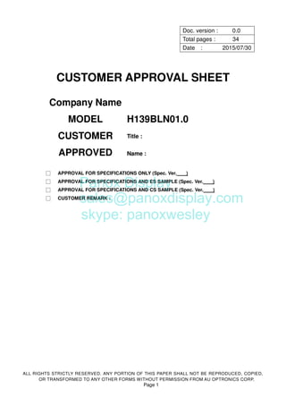
  • 1. ALL RIGHTS STRICTLY RESERVED. ANY PORTION OF THIS PAPER SHALL NOT BE REPRODUCED, COPIED, OR TRANSFORMED TO ANY OTHER FORMS WITHOUT PERMISSION FROM AU OPTRONICS CORP. Page 1 Doc. version : 0.0 Total pages : 34 Date : 2015/07/30 CUSTOMER APPROVAL SHEET Company Name MODEL H139BLN01.0 CUSTOMER APPROVED Title : Name : □ APPROVAL FOR SPECIFICATIONS ONLY (Spec. Ver. ) □ APPROVAL FOR SPECIFICATIONS AND ES SAMPLE (Spec. Ver. ) □ APPROVAL FOR SPECIFICATIONS AND CS SAMPLE (Spec. Ver. ) □ CUSTOMER REMARK : Panox Display sales@panoxdisplay.com skype: panoxwesley
  • 2. Version 0.0 Page: 2/34 ALL RIGHTS STRICTLY RESERVED. ANY PORTION OF THIS PAPER SHALL NOT BE REPRODUCED, COPIED, OR TRANSFORMED TO ANY OTHER FORMS WITHOUT PERMISSION FROM AU OPTRONICS CORP. Page 2 Product Specification 1.39" AMOLED MODEL NAME: H139BLN01.0 AUO Product P/N: 95.01H73.000 < >Preliminary Specification◆ < >Final Specification Note: The content of this specification is subject to change. © 2015 AU Optronics All Rights Reserved, Do Not Copy. Panox Display sales@panoxdisplay.com skype: panoxwesley
  • 3. Version 0.0 Page: 3/34 3 ALL RIGHTS STRICTLY RESERVED. ANY PORTION OF THIS PAPER SHALL NOT BE REPRODUCED, COPIED, OR TRANSFORMED TO ANY OTHER FORMS WITHOUT PERMISSION FROM AU OPTRONICS CORP. Record of Revision Version Revise Date Page Content 0.0 May 26, 2015 First Draft Panox Display sales@panoxdisplay.com skype: panoxwesley
  • 4. Version 0.0 Page: 4/34 4 ALL RIGHTS STRICTLY RESERVED. ANY PORTION OF THIS PAPER SHALL NOT BE REPRODUCED, COPIED, OR TRANSFORMED TO ANY OTHER FORMS WITHOUT PERMISSION FROM AU OPTRONICS CORP. Contents A. General Specification ......................................................................................................................................5 1. Physical Specifications.............................................................................................................................5 2. FPC Pin Assignment..................................................................................................................................5 3. Absolute Maximum Ratings......................................................................................................................7 B. DC Characteristics...........................................................................................................................................8 1. Display DC Characteristics.......................................................................................................................8 2. Display Current Consumption..................................................................................................................9 C. AC Characteristics .........................................................................................................................................10 1. MIPI Interface Characteristics ...................................................................................10 2. Display RESET Timing Characteristics ....................................................................12 3 Operating Sequence................................................................................................................................14 D. Power IC Application Circuit.........................................................................................................................17 E. Display Scan Direction & Coordinate...........................................................................................................17 F. Optical Specifications ....................................................................................................................................23 G. Reliability Test Items......................................................................................................................................31 H. Packing............................................................................................................................................................32 I. Outline Demension.........................................................................................................................................33 J. Precaution .......................................................................................................................................................34 Panox Display sales@panoxdisplay.com skype: panoxwesley
  • 5. Version 0.0 Page: 5/34 5 ALL RIGHTS STRICTLY RESERVED. ANY PORTION OF THIS PAPER SHALL NOT BE REPRODUCED, COPIED, OR TRANSFORMED TO ANY OTHER FORMS WITHOUT PERMISSION FROM AU OPTRONICS CORP. A. General Specification 1. Physical Specifications No. Item Specification Unit Remark 1 Display Size 1.4 Inch 2 ITO Technology Type LTPS 3 Display Type AMOLED 4 Resolution 400RGB*400 5 Color Depth 16.7M 6 Viewing Direction All direction Note 1 7 Contrast Ratio 10000:1 Min 8 Luminance 350cd/m2 cd/m 2 Typ 9 Panel Size 40.5(H)+38.6(W)+0.7(T) mm Note 1 10 Panel Maximum Thickness 0.8 mm Note 1 11 Panel Active Area ¢35.4 mm Diameter 12 Pixel Size 88.5*88.5 µm 13 Pixel Pitch 88.5 µm 14 Pixel Aspect Ratio 1:1 15 Driver IC Recommended by supplier 16 Driver IC RAM Size Full RAM 17 Light Source OLED 18 Interface MIPI 19 Operation Temperature -20~70 degC 20 Storage Temperature -30~80 degC 21 Weight 2.15 Gram ±15% 22 Pixel Per inch 286 PPI 23 Environmental Protection Requirement RoHS & REACH must be executed 24 Connection method MOLEX :5042482410 Part No. 25 Gamma Correction R/G/B separation Hard coat treating 3H26 Polarizer Type Glare 27 Panel gate scan direction W/O Note 2 28 Warpage Front side warpage value < 0.1mm Rear side warpage value(w/o foam) < 0.1mm Note 3 Note1:Please Refer to the mechanical drawing. Note2:Some GOP panel can not support gate bidirectional scanning , or even some gate bidirectional scanning GOP panel are abnormal working when the gate scanning direction set to be reversed. Panox Display sales@panoxdisplay.com skype: panoxwesley
  • 6. Version 0.0 Page: 6/34 6 ALL RIGHTS STRICTLY RESERVED. ANY PORTION OF THIS PAPER SHALL NOT BE REPRODUCED, COPIED, OR TRANSFORMED TO ANY OTHER FORMS WITHOUT PERMISSION FROM AU OPTRONICS CORP. Note3: Warpage inspected by 3D coordinate scanning/ measuring system to analyze surface warpage and precision gauge is applied for module thickness measurement. OLED is placed on flat stage to get 4 points warpage measured by 3D scanning system or gauge.(4 points position is defined same as Uniformity in note 9) Test Method: Nikon VMR-3020- optical or other useful method. 2. FPC Pin Assignment Main FPC Pin assignment — AMOLED Panel Input/Output Signal Interfac FPCA recommended connector: 504248-2410,Molex Main board recommended connector: 504208-2410,Molex Pin No. Symbol I/O Function Remark 1 GND Power Ground 2 XRES I Device reset signal (0 : enable ; 1 : Disable) 3 DSI_D0N I/O MIPI negative data signal 4 SWIRE O SWIRE signal for PWR IC control 5 DSI_D0P I/O MIPI positive data signal 6 NC - Floating 7 GND Power Ground 8 TE I Vsync (vertical sync) signal output from panel to avoid tearing effect 9 DSI_CLKN I MIPI negative clock signal 10 GND Power Ground 11 DSI_CLKP I MIPI positive clock signal 12 GND Power Ground 13 GND Power Ground 14 GND Power Ground 15 VDDIO Power Power supply for interface system excep MIPI interface 16 VCI Power Driver analog power supply 17 GND Power Ground 18 GND Power Ground 19 ELVSS Power AMOLED negative power supply 20 ELVDD Power AMOLED positive power supply 21 ELVSS Power AMOLED negative power supply 22 ELVDD Power AMOLED positive power supply 23 ELVSS Power AMOLED negative power supply 24 ELVDD Power AMOLED positive power supply Note: I = input ; O = output ; P = Power ; I/O = input / Output; NC= No Connection Panox Display sales@panoxdisplay.com skype: panoxwesley
  • 7. Version 0.0 Page: 7/34 7 ALL RIGHTS STRICTLY RESERVED. ANY PORTION OF THIS PAPER SHALL NOT BE REPRODUCED, COPIED, OR TRANSFORMED TO ANY OTHER FORMS WITHOUT PERMISSION FROM AU OPTRONICS CORP. 3. Absolute Maximum Ratings Item Symbol Min. Max. Unit Remark Digital Power Supply VDDIO -0.3 5.5 V Analog Power Supply VCI -0.3 5.5 V ELVDD power Supply ELVDD - 5.0 V ELVSS power Supply ELVSS -5.0 - V Note : If the module exceeds the absolute maximum ratings, it may be damaged permanently. Panox Display sales@panoxdisplay.com skype: panoxwesley
  • 8. Version 0.0 Page: 8/34 8 ALL RIGHTS STRICTLY RESERVED. ANY PORTION OF THIS PAPER SHALL NOT BE REPRODUCED, COPIED, OR TRANSFORMED TO ANY OTHER FORMS WITHOUT PERMISSION FROM AU OPTRONICS CORP. B. DC Characteristics 1. Display DC Characteristics Item Symbol Min. Typ. Max. Unit Remark Digital Power Supply VDDIO 1.65 1.8 1.95 V Note1 Analog Power Supply VCI 2.7 2.8 2.9 V Note1 ELVDD power Supply ELVDD 4.55 4.60 4.65 V Note1 ELVSS power Supply ELVSS -2.35 -2.40 -2.45 V Note1 H Level VIH 0.8* VDDIO - VDDIO VInput Signal Voltage L Level VIL 0 - 0.2* VDDIO V Note1 H Level VOH 0.8* VDDIO - VDDIO V Note1Output Signal Voltage L Level VOL 0 - 0.2* VDDIO V Note1 Note 1: The operation is guaranteed under the recommended operating conditions only. The operation is not guaranteed if a quick voltage change occurs during the operation. To prevent the noise, a bypass capacitor must be inserted into the line closed to the power pin. Panox Display sales@panoxdisplay.com skype: panoxwesley
  • 9. Version 0.0 Page: 9/34 9 ALL RIGHTS STRICTLY RESERVED. ANY PORTION OF THIS PAPER SHALL NOT BE REPRODUCED, COPIED, OR TRANSFORMED TO ANY OTHER FORMS WITHOUT PERMISSION FROM AU OPTRONICS CORP. 2. Display Current Consumption Power Supply: IOVCC=1.8V VCI=2.8V Frame Frequency: Fframe >=60HZ @ 25degC, Brightness 350 nits Spec Typ Max Display Mode Item Symbol Current(mA) Current(mA) Current of IOVDD Idd 2.2 2.5 Current of VCI Ici 4.2 4.6 100% Pixel On (Normal mode) Current of ELVSS Iess 21 23.4 Current of IOVDD Idd 2.2 2.5 Current of VCI Ici 4.4 4.9 50% Pixel On (Normal mode) Current of ELVSS Iess 10.5 11.7 Current of IOVDD Idd 2.2 2.5 Current of VCI Ici 4.6 5.3 All Pixel Off (Normal mode ) Current of ELVSS Iess 0.0 0.0 Current of IOVDD Idd -- 0.0 Current of VCI Ici -- <2uA All Pixel Off (Standby mode) Current of ELVSS Iess -- 0.0 Power Supply: IOVCC=1.8V VCI=2.8V Frame Frequency: Fframe =15HZ @ 25degC, Brightness 20 nits Spec Typ Max Display Mode Item Symbol Current(mA) Current(mA) Current of IOVDD Idd 1.2 1.3 Current of VCI Ici 2.4 2.7 10% Pixel On (Idle mode) Current of ELVSS Iess 0 0 Panox Display sales@panoxdisplay.com skype: panoxwesley
  • 10. Version 0.0 Page: 10/34 10 ALL RIGHTS STRICTLY RESERVED. ANY PORTION OF THIS PAPER SHALL NOT BE REPRODUCED, COPIED, OR TRANSFORMED TO ANY OTHER FORMS WITHOUT PERMISSION FROM AU OPTRONICS CORP. C. AC Characteristics 1. MIPI Interface Characteristics HS Data Transmission Burst HS clock transmission Turnaround Procedure Panox Display sales@panoxdisplay.com skype: panoxwesley
  • 11. Version 0.0 Page: 11/34 11 ALL RIGHTS STRICTLY RESERVED. ANY PORTION OF THIS PAPER SHALL NOT BE REPRODUCED, COPIED, OR TRANSFORMED TO ANY OTHER FORMS WITHOUT PERMISSION FROM AU OPTRONICS CORP. Bus turnaround (BAT) from MPU to display module timing Timing Parameters Symbol Description Min Typ Max Unit TCLK-POST Time that the transmitter continues to send HS clock after the last associated Data Lane has transitioned to LP Mode. Interval is defined as the period from the end of THS- TRAIL to the beginning of TCLK-TRAIL . 60ns + 52*UI ns TCLK-TRAIL Time that the transmitter drives the HS-0 state after the last payload clock bit of a HS transmission burst. 60 ns THS-EXIT Time that the transmitter drives LP-11 following a HS burst. 300 ns TCLK-TERM-EN Time for the Clock Lane receiver to enable the HS line termination, starting from the time point when Dn crosses VIL,MAX . Time for Dn to reach VTERM- EN 38 ns TCLK-PREPARE Time that the transmitter drives the Clock Lane LP-00 Line state immediately before the HS-0 Line state starting the HS transmission. 38 95 ns TCLK-PRE Time that the HS clock shall be driven by the transmitter prior to any associated Data Lane beginning the transition from LP to HS mode. 8 UI TCLK-PREPARE + TCLK-ZERO TCLK-PREPARE + time that the transmitter drives the HS-0 state prior to starting the Clock. 300 ns TD-TERM-EN Time for the Data Lane receiver to enable the HS line termination, starting from the time point when Dn crosses VIL,MAX . Time for Dn to Reach VTERM- EN 35 ns +4*UI THS-PREPARE Time that the transmitter drives the Data Lane LP-00 Line state immediately before 40ns + 4*UI 85 ns + 6*UI ns Panox Display sales@panoxdisplay.com skype: panoxwesley
  • 12. Version 0.0 Page: 12/34 12 ALL RIGHTS STRICTLY RESERVED. ANY PORTION OF THIS PAPER SHALL NOT BE REPRODUCED, COPIED, OR TRANSFORMED TO ANY OTHER FORMS WITHOUT PERMISSION FROM AU OPTRONICS CORP. the HS-0 Line state starting the HS transmission THS-PREPARE + THS-ZERO THS-PREPARE + time that the transmitter drives the HS-0 state prior to transmitting the Sync sequence. 145ns + 10*UI ns THS-TRAIL Time that the transmitter drives the flipped differential state after last payload data bit of a HS transmission burst 60ns + 4*UI ns TLPX(M) Transmitted length of any Low-Power state period of MCU to display module 50 150 ns TTA-SURE(M) Time that the display module waits after the LP-10 state before transmitting the Bridge state (LP-00) during a Link Turnaround. TLPX(M) 2*TLPX(M) ns TLPX(D) Transmitted length of any Low-Power state period of display module to MCU 50 150 ns TTA-GET(D) Time that the display module drives the Bridge state (LP-00) after accepting control during a Link Turnaround. 5*TLPX(D) ns TTA-GO(D) Time that the display module drives the Bridge state (LP-00) before releasing control during a Link Turnaround. 4*TLPX(D) ns TTA-SURE(D) Time that the MPU waits after the LP-10 state before transmitting the Bridge state (LP-00) during a Link Turnaround. TLPX(D) 2*TLPX(D) ns 2. Display RESET Timing Characteristics Reset input timing Timing Parameters Symbol Parameter Related Pins MIN TYP MAX Note Unit tRESW *1) Reset low pulse width RESX 10 - - - µs - - - 5 When reset applied during Sleep in mode ms tREST *2) Reset complete time - - 120 When reset applied during Sleep out mode ms Panox Display sales@panoxdisplay.com skype: panoxwesley
  • 13. Version 0.0 Page: 13/34 13 ALL RIGHTS STRICTLY RESERVED. ANY PORTION OF THIS PAPER SHALL NOT BE REPRODUCED, COPIED, OR TRANSFORMED TO ANY OTHER FORMS WITHOUT PERMISSION FROM AU OPTRONICS CORP. Note 1. Spike due to an electrostatic discharge on RESX line does not cause irregular system reset according to the table below. RESX Pulse Action Shorter than 5µs Invalid Reset Longer than 15µs Valid Reset Between 5µs and 15µs Reset Initialigation Precedure Note 2. During the resetting period, the display will be blanked (The display is entering blanking sequence, which maximum time is 120 ms, when Reset Starts in Sleep Out –mode. The display remains the blank state in Sleep In –mode) and then return to Default condition for H/W reset. Note 3. During Reset Complete Time, data in OTP will be latched to internal register during this period. This loading is done every time when there is H/W reset complete time (tREST) within 5ms after a rising edge of RESX. Note 4. Spike Rejection also applies during a valid reset pulse as shown below: Note 5. It is necessary to wait 5msec after releasing RESX before sending commands. Also Sleep Out command cannot be sent for 120msec. TE Timing Characteristics tvdh = The display is not updated from the frame memory tvdl = The display is updated from the frame memory MIPI Initial CMD Flow Panox Display sales@panoxdisplay.com skype: panoxwesley
  • 14. Version 0.0 Page: 14/34 14 ALL RIGHTS STRICTLY RESERVED. ANY PORTION OF THIS PAPER SHALL NOT BE REPRODUCED, COPIED, OR TRANSFORMED TO ANY OTHER FORMS WITHOUT PERMISSION FROM AU OPTRONICS CORP. Operating Sequence Display Power on/off Sequence Power on sequence Power off sequence Panox Display sales@panoxdisplay.com skype: panoxwesley
  • 15. Version 0.0 Page: 15/34 15 ALL RIGHTS STRICTLY RESERVED. ANY PORTION OF THIS PAPER SHALL NOT BE REPRODUCED, COPIED, OR TRANSFORMED TO ANY OTHER FORMS WITHOUT PERMISSION FROM AU OPTRONICS CORP. Display Initial Setting Recommended Power on Initial Sequence Address Step Instruction/Parameters Delay time R/W MIPI Data Type MIPI Others Data hex. Description 1 Turn on VCI VCI=2.8V 2 Turn on VDDIO VDDIO=1.8V 3 Delay no limit 4 REST pin low 20us 5 REST pin high 6 Delay 5 ms 7 W 0x15 FE FE00 07 8 W 0x15 07 07A0 4F 9 W 0x15 FE FE00 0A 10 W 0x15 1C 1CD0 1B 11 W 0x15 FE FE00 00 12 W 0x15 35 3500 00 13 Sleep out W 0x05 11 1100 00 14 Turn on peripheral packet 0x32 Video Turn On 15 Delay 300 ms 16 Display on W 0x05 29 2900 00 Recommended Power off Mode Sequence Address Step Instruction/Parameters Delay time R/W MIPI Data Type MIPI Others Data hex. Description 1 Display Off W 0x05 28 2800 00 2 Sleep in W 0x05 10 1000 00 3 delay 120ms 4 Power off Panox Display sales@panoxdisplay.com skype: panoxwesley
  • 16. Version 0.0 Page: 16/34 16 ALL RIGHTS STRICTLY RESERVED. ANY PORTION OF THIS PAPER SHALL NOT BE REPRODUCED, COPIED, OR TRANSFORMED TO ANY OTHER FORMS WITHOUT PERMISSION FROM AU OPTRONICS CORP. Idle mode Flow (1) Normal to Idle Recommended Idle Initial Sequence Address Step Instruction/Parameters Delay time R/W MIPI Data Type MIPI Others Data hex. Description 1 Enter Idle mode W 0x05 39 3900 00 Idle mode 15HZ (2) Idle to Normal Recommended Power on Initial Sequence Address Step Instruction/Parameters Delay time R/W MIPI Data Type MIPI Others Data hex. Description 1 Idle mode Off W 0x05 38 3800 00 Normal mode 60HZ Brightness Control Recommended Brightness Control Address Instruction/Parameters Delay time R/W MIPI Data Type MIPI Others Data hex. Description Brightness control W 0x05 51 5100 Value Value form 0~255(FF) Panox Display sales@panoxdisplay.com skype: panoxwesley
  • 17. Version 0.0 Page: 17/34 17 ALL RIGHTS STRICTLY RESERVED. ANY PORTION OF THIS PAPER SHALL NOT BE REPRODUCED, COPIED, OR TRANSFORMED TO ANY OTHER FORMS WITHOUT PERMISSION FROM AU OPTRONICS CORP. D. Power IC Application Circuit E. Display Scan Direction & Coordinate Panel Start Point = (0 , 0) Panel End Point = (399 , 399) Each Line = (Start x , y) ~~ (End x , y) Panox Display sales@panoxdisplay.com skype: panoxwesley
  • 18. Version 0.0 Page: 18/34 18 ALL RIGHTS STRICTLY RESERVED. ANY PORTION OF THIS PAPER SHALL NOT BE REPRODUCED, COPIED, OR TRANSFORMED TO ANY OTHER FORMS WITHOUT PERMISSION FROM AU OPTRONICS CORP. Coordinate Y start_X end_X Total Y start_X end_X Total Y start_X end_X Total 0 187 212 26 30 94 305 212 60 57 342 286 1 176 223 48 31 92 307 216 61 56 343 288 2 169 230 62 32 91 308 218 62 55 344 290 3 163 236 74 33 89 310 222 63 54 345 292 4 158 241 84 34 88 311 224 64 53 346 294 5 154 245 92 35 86 313 228 65 52 347 296 6 150 249 100 36 85 314 230 66 51 348 298 7 146 253 108 37 84 315 232 67 50 349 300 8 143 256 114 38 82 317 236 68 49 350 302 9 139 260 122 39 81 318 238 69 49 350 302 10 136 263 128 40 79 320 242 70 48 351 304 11 133 266 134 41 78 321 244 71 47 352 306 12 131 268 138 42 77 322 246 72 46 353 308 13 128 271 144 43 76 323 248 73 45 354 310 14 125 274 150 44 74 325 252 74 44 355 312 15 123 276 154 45 73 326 254 75 44 355 312 16 121 278 158 46 72 327 256 76 43 356 314 17 118 281 164 47 71 328 258 77 42 357 316 18 116 283 168 48 70 329 260 78 41 358 318 19 114 285 172 49 68 331 264 79 40 359 320 20 112 287 176 50 67 332 266 80 40 359 320 21 110 289 180 51 66 333 268 81 39 360 322 22 108 291 184 52 65 334 270 82 38 361 324 23 106 293 188 53 64 335 272 83 38 361 324 24 104 295 192 54 63 336 274 84 37 362 326 25 102 297 196 55 62 337 276 85 36 363 328 26 101 298 198 56 61 338 278 86 35 364 330 27 99 300 202 57 60 339 280 87 35 364 330 28 97 302 206 58 59 340 282 88 34 365 332 29 96 303 208 59 58 341 284 89 33 366 334 Panox Display sales@panoxdisplay.com skype: panoxwesley
  • 19. Version 0.0 Page: 19/34 19 ALL RIGHTS STRICTLY RESERVED. ANY PORTION OF THIS PAPER SHALL NOT BE REPRODUCED, COPIED, OR TRANSFORMED TO ANY OTHER FORMS WITHOUT PERMISSION FROM AU OPTRONICS CORP. Y start_X end_X Total Y start_X end_X Total Y start_X end_X Total 90 33 366 334 120 17 382 366 150 6 393 388 91 32 367 336 121 16 383 368 151 6 393 388 92 31 368 338 122 16 383 368 152 6 393 388 93 31 368 338 123 15 384 370 153 6 393 388 94 30 369 340 124 15 384 370 154 5 394 390 95 30 369 340 125 14 385 372 155 5 394 390 96 29 370 342 126 14 385 372 156 5 394 390 97 28 371 344 127 14 385 372 157 5 394 390 98 28 371 344 128 13 386 374 158 4 395 392 99 27 372 346 129 13 386 374 159 4 395 392 100 27 372 346 130 13 386 374 160 4 395 392 101 26 373 348 131 12 387 376 161 4 395 392 102 25 374 350 132 12 387 376 162 4 395 392 103 25 374 350 133 11 388 378 163 3 396 394 104 24 375 352 134 11 388 378 164 3 396 394 105 24 375 352 135 11 388 378 165 3 396 394 106 23 376 354 136 10 389 380 166 3 396 394 107 23 376 354 137 10 389 380 167 3 396 394 108 22 377 356 138 10 389 380 168 3 396 394 109 22 377 356 139 9 390 382 169 2 397 396 110 21 378 358 140 9 390 382 170 2 397 396 111 21 378 358 141 9 390 382 171 2 397 396 112 20 379 360 142 9 390 382 172 2 397 396 113 20 379 360 143 8 391 384 173 2 397 396 114 19 380 362 144 8 391 384 174 2 397 396 115 19 380 362 145 8 391 384 175 2 397 396 116 18 381 364 146 7 392 386 176 1 398 398 117 18 381 364 147 7 392 386 177 1 398 398 118 17 382 366 148 7 392 386 178 1 398 398 119 17 382 366 149 7 392 386 179 1 398 398 Panox Display sales@panoxdisplay.com skype: panoxwesley
  • 20. Version 0.0 Page: 20/34 20 ALL RIGHTS STRICTLY RESERVED. ANY PORTION OF THIS PAPER SHALL NOT BE REPRODUCED, COPIED, OR TRANSFORMED TO ANY OTHER FORMS WITHOUT PERMISSION FROM AU OPTRONICS CORP. Y start_X end_X Total Y start_X end_X Total Y start_X end_X Total 180 1 398 398 210 0 399 400 240 4 395 392 181 1 398 398 211 0 399 400 241 4 395 392 182 1 398 398 212 0 399 400 242 5 394 390 183 1 398 398 213 1 398 398 243 5 394 390 184 1 398 398 214 1 398 398 244 5 394 390 185 1 398 398 215 1 398 398 245 5 394 390 186 1 398 398 216 1 398 398 246 6 393 388 187 0 399 400 217 1 398 398 247 6 393 388 188 0 399 400 218 1 398 398 248 6 393 388 189 0 399 400 219 1 398 398 249 6 393 388 190 0 399 400 220 1 398 398 250 7 392 386 191 0 399 400 221 1 398 398 251 7 392 386 192 0 399 400 222 1 398 398 252 7 392 386 193 0 399 400 223 1 398 398 253 7 392 386 194 0 399 400 224 2 397 396 254 8 391 384 195 0 399 400 225 2 397 396 255 8 391 384 196 0 399 400 226 2 397 396 256 8 391 384 197 0 399 400 227 2 397 396 257 9 390 382 198 0 399 400 228 2 397 396 258 9 390 382 199 0 399 400 229 2 397 396 259 9 390 382 200 0 399 400 230 2 397 396 260 9 390 382 201 0 399 400 231 3 396 394 261 10 389 380 202 0 399 400 232 3 396 394 262 10 389 380 203 0 399 400 233 3 396 394 263 10 389 380 204 0 399 400 234 3 396 394 264 11 388 378 205 0 399 400 235 3 396 394 265 11 388 378 206 0 399 400 236 3 396 394 266 11 388 378 207 0 399 400 237 4 395 392 267 12 387 376 208 0 399 400 238 4 395 392 268 12 387 376 209 0 399 400 239 4 395 392 269 13 386 374 Panox Display sales@panoxdisplay.com skype: panoxwesley
  • 21. Version 0.0 Page: 21/34 21 ALL RIGHTS STRICTLY RESERVED. ANY PORTION OF THIS PAPER SHALL NOT BE REPRODUCED, COPIED, OR TRANSFORMED TO ANY OTHER FORMS WITHOUT PERMISSION FROM AU OPTRONICS CORP. Y start_X end_X Total Y start_X end_X Total Y start_X end_X Total 270 13 386 374 300 27 372 346 330 49 350 302 271 13 386 374 301 28 371 344 331 49 350 302 272 14 385 372 302 28 371 344 332 50 349 300 273 14 385 372 303 29 370 342 333 51 348 298 274 14 385 372 304 30 369 340 334 52 347 296 275 15 384 370 305 30 369 340 335 53 346 294 276 15 384 370 306 31 368 338 336 54 345 292 277 16 383 368 307 31 368 338 337 55 344 290 278 16 383 368 308 32 367 336 338 56 343 288 279 17 382 366 309 33 366 334 339 57 342 286 280 17 382 366 310 33 366 334 340 58 341 284 281 17 382 366 311 34 365 332 341 59 340 282 282 18 381 364 312 35 364 330 342 60 339 280 283 18 381 364 313 35 364 330 343 61 338 278 284 19 380 362 314 36 363 328 344 62 337 276 285 19 380 362 315 37 362 326 345 63 336 274 286 20 379 360 316 38 361 324 346 64 335 272 287 20 379 360 317 38 361 324 347 65 334 270 288 21 378 358 318 39 360 322 348 66 333 268 289 21 378 358 319 40 359 320 349 67 332 266 290 22 377 356 320 40 359 320 350 68 331 264 291 22 377 356 321 41 358 318 351 70 329 260 292 23 376 354 322 42 357 316 352 71 328 258 293 23 376 354 323 43 356 314 353 72 327 256 294 24 375 352 324 44 355 312 354 73 326 254 295 24 375 352 325 44 355 312 355 74 325 252 296 25 374 350 326 45 354 310 356 76 323 248 297 25 374 350 327 46 353 308 357 77 322 246 298 26 373 348 328 47 352 306 358 78 321 244 299 27 372 346 329 48 351 304 359 79 320 242 Panox Display sales@panoxdisplay.com skype: panoxwesley
  • 22. Version 0.0 Page: 22/34 22 ALL RIGHTS STRICTLY RESERVED. ANY PORTION OF THIS PAPER SHALL NOT BE REPRODUCED, COPIED, OR TRANSFORMED TO ANY OTHER FORMS WITHOUT PERMISSION FROM AU OPTRONICS CORP. Y start_X end_X Total Y start_X end_X Total Y start_X end_X Total 360 81 318 238 390 139 260 122 361 82 317 236 391 143 256 114 362 84 315 232 392 146 253 108 363 85 314 230 393 150 249 100 364 86 313 228 394 154 245 92 365 88 311 224 395 158 241 84 366 89 310 222 396 163 236 74 367 91 308 218 397 169 230 62 368 92 307 216 398 176 223 48 369 94 305 212 399 187 212 26 370 96 303 208 371 97 302 206 372 99 300 202 373 101 298 198 374 102 297 196 375 104 295 192 376 106 293 188 377 108 291 184 378 110 289 180 379 112 287 176 380 114 285 172 381 116 283 168 382 118 281 164 383 121 278 158 384 123 276 154 385 125 274 150 386 128 271 144 387 131 268 138 388 133 266 134 389 136 263 128 Panox Display sales@panoxdisplay.com skype: panoxwesley
  • 23. Version 0.0 Page: 23/34 23 ALL RIGHTS STRICTLY RESERVED. ANY PORTION OF THIS PAPER SHALL NOT BE REPRODUCED, COPIED, OR TRANSFORMED TO ANY OTHER FORMS WITHOUT PERMISSION FROM AU OPTRONICS CORP. F. Optical Specifications Test condition::::IOVCC=1.8V , VCI=2.8V ,Ta=25℃℃℃℃ AUO Spec Item Symbol Condition Min Typ Max Unit Note luminance Bp θ=0°ɸ=0° 300 350 -- cd/m2 CPK>1.33 Note1 Uniformity Bp△ 85 -- -- % Note2 Left θL 80 -- -- Right θR 80 -- -- Top ψT 80 -- -- Viewing Angle Bottom ψB Cr≥10 80 -- -- deg Note 3 Contrast Ratio Cr θ=0°ɸ=0° 10000 -- - Note 4 Tr -- 2 3 ms Tf -- 2 3 msResponse Time Tgray - 2 3 ms Note 5 x 0.645 0.675 0.705 Red y 0.295 0.325 0.355 x 0.186 0.236 0.286 Green y 0.661 0.711 0.761 x 0.09 0.13 0.17 Blue y 0.025 0.065 0.105 x 0.28 0.3 0.32 Color Coordina te of CIE1931 White y θ=0°ɸ=0° 0.29 0.31 0.33 - Note 6 NTSC Ratio NTSC CIE1931 100 -- % Note 7 Color temperature CT 7500 K Flicker amount - - -- -30 dB Note 8 Gamma - - 1.9 2.2 2.5 Note 9 Crosstalk CT△ - - -- 1.1 Note 10 Reflectance Rf @550nm -- TBD -- % Note 11 Polarization direction of front polarizer PdF -- 135 -- deg Note 12 θL=30° 35 40 % θR=30° 35 40 % ψT=30° 35 40 % Luminance decrease ratio of full white ψB=30° 35 40 % Note 13 θL=30° --- 3 4 JNCDColor shift θR=30° --- 3 4 JNCD Note 14 Panox Display sales@panoxdisplay.com skype: panoxwesley
  • 24. Version 0.0 Page: 24/34 24 ALL RIGHTS STRICTLY RESERVED. ANY PORTION OF THIS PAPER SHALL NOT BE REPRODUCED, COPIED, OR TRANSFORMED TO ANY OTHER FORMS WITHOUT PERMISSION FROM AU OPTRONICS CORP. ψT=30° -- 3 4 JNCD ψB=30° -- 3 4 JNCD OLED lifetime 0.95*(TY P brightnes s) At 25 ,with℃ white color pattern 150 - hrs Tentative Image sticking With 8*8 black-white chess board test image, lighting on with maximum luminance for 12H Light off or gray display for 3 minutes, normal performance after the test, without image sticking. Tentative Note 1: Luminance measurement The test condition is at 25℃ and measured on the surface of OLED module. • The data are measured after OLEDs are lighted on for more than 5 minutes and displays are fully white. The brightness is the average value of 5 measured spots. Measurement equipment CS2000 or similar equipments (Field of view:1deg,Distance:50cm) • Measuring surroundings: Dark room. • Measuring temperature: Ta=25℃. • Adjust operating voltage to get optimum contrast at the center of the display. • Measured value at the center point of panel must be after more than 5 minutes while backlight turning on. Note 2: Uniformity • The test condition is at 25℃and measured on the surface of display module. • Measurement equipment: CS2000 or similar equipments. • The luminance uniformity is calculated by using following formula: • △Bp = Bp (Min.) / Bp (Max.)×100 (%) Panox Display sales@panoxdisplay.com skype: panoxwesley
  • 25. Version 0.0 Page: 25/34 25 ALL RIGHTS STRICTLY RESERVED. ANY PORTION OF THIS PAPER SHALL NOT BE REPRODUCED, COPIED, OR TRANSFORMED TO ANY OTHER FORMS WITHOUT PERMISSION FROM AU OPTRONICS CORP. • Bp (Max.) = Maximum brightness in 5 measured spots • Bp (Min.) = Minimum brightness in 5 measured spots. Note 3: The definition of Viewing Angle Refer to the graph below marked by è and Ô Note 4: The definition of Contrast Ratio (Test OLED using CS2000 or similar equipments): Luminance When OLED is at “White” state Contrast Ratio(CR)= Luminance When OLED is at “Black” state (Contrast Ratio is measured in optimum common electrode voltage) Note 5: Definition of Response time. (Test OLED using DMS501 or similar equipments): Panox Display sales@panoxdisplay.com skype: panoxwesley
  • 26. Version 0.0 Page: 26/34 26 ALL RIGHTS STRICTLY RESERVED. ANY PORTION OF THIS PAPER SHALL NOT BE REPRODUCED, COPIED, OR TRANSFORMED TO ANY OTHER FORMS WITHOUT PERMISSION FROM AU OPTRONICS CORP. The output signals of photo detector are measured when the input signals are changed from “black” to “white”(Voltage falling time) and from “white” to “black”(Voltage rising time), respectively. The response time is defined as the time interval between the 10% and 90% of amplitudes. Refer to figure as below. Response time of gray to gray: • Measurement equipment: DMS501 or similar equipments. • Test method :we define 8 grays L0-L7, the grays of L0-L7 were defined as:0,36,73, 109, 146, 182, 219, 255. The output signals of photo detector are measured when the input signals are changed from “Lx” to “Ly”, x, y= [0, 7]. The response time is defined as the time interval between the 10% and 90% of amplitudes. The result of the test can be noted as below: L0 L1 L2 L3 L4 L5 L6 L7 L0 L1 L2 L3 L4 L5 L6 L7 Note 6: Color Coordinates of CIE 1931 • The test condition is at 25℃and measured on the surface of display module. • Measurement equipment: CS2000 or similar equipments. • The Color Coordinate (CIE 1931) is the measurement of the center of the display shown in below figure. Note 7: Definition of Color of CIE Coordinate and NTSC Ratio. Panox Display sales@panoxdisplay.com skype: panoxwesley
  • 27. Version 0.0 Page: 27/34 27 ALL RIGHTS STRICTLY RESERVED. ANY PORTION OF THIS PAPER SHALL NOT BE REPRODUCED, COPIED, OR TRANSFORMED TO ANY OTHER FORMS WITHOUT PERMISSION FROM AU OPTRONICS CORP. 100% triangleNTSCofarea triangleRGBofarea S ×= Note 8: Flicker • Measurement equipment :CA-210 or similar equipments • Measuring temperature: Ta=25℃. • Test method: JEITA method • Test pattern : Refer to below(Test Pattern should be full-fill of display screen) 1 Dot Inversion 2 Dot inversion Line Inversion Frame Inversion The point should be marked is, for line and frame inversion, the background of Flicker Test Pattern- “gray “ are defined as middle gray scale .For example, RGB 24bit “gray” defined as below: For Dot inversion, the RGB data for first pixel is (127, 0, 127), the RGB data for the second pixel is (0, 127, 0). • Frame Frequency Requirement before test: The OLED must be tuned to more than 65HZ before measurement . Panox Display sales@panoxdisplay.com skype: panoxwesley
  • 28. Version 0.0 Page: 28/34 28 ALL RIGHTS STRICTLY RESERVED. ANY PORTION OF THIS PAPER SHALL NOT BE REPRODUCED, COPIED, OR TRANSFORMED TO ANY OTHER FORMS WITHOUT PERMISSION FROM AU OPTRONICS CORP. • Measurement Point: the center of display active area. • Conversion of Flicker ratio: Flicker[dB] = 10xlog[Px/P0] Where Px: Maximum power spectrum of AC component after passing through integrator P0:Power spectrum of DC component after passing through integrator AC component=b (Refer to below diagram ) DC component=a (Refer to below diagram) Note 9: gamma curve control • For gamma curve control, HUAWEI’s request as below: • 1,the whole curve’s tolerance must control within +/-0.3, HUAWEI will test the gray scale below: 0, 8, 16, 25, 33, 41, 49, 58, 66, 74, 82, 90, 99, 107, 115, 123, 132, 140, 148, 156, 165, 173, 181, 189, 197,206, 214, 222, 230, 239, 247, 255 Note 10: Crosstalk • There should be no visible cross-talk in normal direction of the display when the two ”Cross-talk Test Patterns ” below are loaded. • Measurement equipment: CS2000 or similar equipments • The point should be marked is, the background of Cross-talk Test Pattern-“gray “ are defined as middle gray scale . For example, RGB 24bit “gray” defined as below: • △Bpn = Bpn (gray) / Bpn (white) Which n means the dot No. In the Cross-talk Test Pattern ; Panox Display sales@panoxdisplay.com skype: panoxwesley
  • 29. Version 0.0 Page: 29/34 29 ALL RIGHTS STRICTLY RESERVED. ANY PORTION OF THIS PAPER SHALL NOT BE REPRODUCED, COPIED, OR TRANSFORMED TO ANY OTHER FORMS WITHOUT PERMISSION FROM AU OPTRONICS CORP. Bpn (gray) means the brightness of the No.n spots in Cross-talk Test Pattern; Bpn (white) means the brightness of the No.n spots in Full white Test Pattern; • △Bp (Max.) = Maximum value in △Bp1~△Bp4. • △Bp (Min.) = Minimum value in △Bp1~△Bp4. • △CT=△Bp (Max.)/ △Bp(Min.). • △CT must be less than 1.10 Cross-talk Test Pattern Note 11:Reflectance Ratio • Measurement equipment : X-rite SP64 • Measurement parameter:Reflectance Ratio @550nm Note 12: Polarization Direction Definition • Viewing direction is normal user viewing direction which is vertical to the display surface • The polarizer which is closer to viewer is defined as Front Polarizer • The polarizer which is on the rear side of viewer is defined as Rear Polarizer • The X axis is defined as parallel line to top&bottom sidelines of the Active Area • PdF which is marked in blue arrow is polarization degree of Front polarizer • The polarization degree parameter must be indicated in range of 0deg to 180deg according to above definition Panox Display sales@panoxdisplay.com skype: panoxwesley
  • 30. Version 0.0 Page: 30/34 30 ALL RIGHTS STRICTLY RESERVED. ANY PORTION OF THIS PAPER SHALL NOT BE REPRODUCED, COPIED, OR TRANSFORMED TO ANY OTHER FORMS WITHOUT PERMISSION FROM AU OPTRONICS CORP. Absorption axis Definition Note 13: Definition of Luminance decrease ratio • Refer to the graph of note 9. • Test pattern : Full White • The luminance decrease ratio is calculated by using following formula: Luminance test at θL/θR/ψT/ψB=30° Luminance decrease Ratio=1- Luminance test at θL/θR/ψT/ψB=0° Note14: Color Shift JNCD • For JNCD measure: • Fix on one pattern like white pattern, • On the condition θ=0 F=0°, we can get the color coordinate (u1', v1') and onθL=30°we can get another color coordinate (u2', v2') • Delta = Square Root( (u2' - u1')^2 + (v2' - v1')^2 ) • JNCD stands for "Just Noticeable Color Difference" • For the (u', v') color space JNCD=0.0040. • 2JNCD means Delta u’v’<0.0080 • For color shift we need to measure white/red/green/blue pattern. This Requirement is from our customer and we have test some of our phone display and the result is OK. Panox Display sales@panoxdisplay.com skype: panoxwesley
  • 31. Version 0.0 Page: 31/34 31 ALL RIGHTS STRICTLY RESERVED. ANY PORTION OF THIS PAPER SHALL NOT BE REPRODUCED, COPIED, OR TRANSFORMED TO ANY OTHER FORMS WITHOUT PERMISSION FROM AU OPTRONICS CORP. G. Reliability Test Items Category No. Test items Conditions Remark 1 High Temp. Operation Ta= 70ºC 240 hrs Reliability (Environment) 2 High Temp. Storage Ta= 80 ºC 240 hrs 3 Low Temp. Operation Ta= -20 ºC 240 hrs 4 Low Temp. Storage Ta= -30 ºC 240 hrs 5 High Temp./Humi. Operation Ta= 60 ºC. 90% RH 240 hrs Reliability (Environment) 6 Thermal Shock -40 ºC ~80 ºC, Dwell for 30 min. 100 cycles. Non-operation Panox Display sales@panoxdisplay.com skype: panoxwesley
  • 32. Version 0.0 Page: 32/34 32 ALL RIGHTS STRICTLY RESERVED. ANY PORTION OF THIS PAPER SHALL NOT BE REPRODUCED, COPIED, OR TRANSFORMED TO ANY OTHER FORMS WITHOUT PERMISSION FROM AU OPTRONICS CORP. H. Packing Panox Display sales@panoxdisplay.com skype: panoxwesley
  • 33. Version 0.0 Page: 33/34 33 ALL RIGHTS STRICTLY RESERVED. ANY PORTION OF THIS PAPER SHALL NOT BE REPRODUCED, COPIED, OR TRANSFORMED TO ANY OTHER FORMS WITHOUT PERMISSION FROM AU OPTRONICS CORP. I. Outline Demension PanoxDisplay sales@panoxdisplay.com skype:panoxwesley
  • 34. Version 0.0 Page: 34/34 34 ALL RIGHTS STRICTLY RESERVED. ANY PORTION OF THIS PAPER SHALL NOT BE REPRODUCED, COPIED, OR TRANSFORMED TO ANY OTHER FORMS WITHOUT PERMISSION FROM AU OPTRONICS CORP. J. Precaution Please pay attention to the following items when you use the OLED Modules(Panel): 1. Do not twist or bend the module(panel) and prevent the unsuitable external force for display during assembly. 2. Adopt measures for good heat radiation. Be sure to use the module(panel) with in the specified temperature. 3. Avoid dust or oil mist during assembly. 4. Follow the correct power sequence while operating. Do not apply the invalid signal, otherwise, it will cause improper shut down and damage the module(panel). 5. Less EMI: it will be more safety and less noise. 6. Please operate module(panel) in suitable temperature. The response time & brightness will drift by different temperature. 7. Avoid to display the fixed pattern (exclude the white pattern) in a long period, otherwise, it will cause image sticking. 8. Please be sure to turn-off the power when connecting or disconnecting the circuit. 9. Polarizer scratches easily, please handle it carefully. 10. Display surface never likes dirt or stains. 11. A dew drop may lead to destruction. Please wipe off any moisture before using module(panel). 12. Sudden temperature changes cause condensation, and it will cause polarizer damaged. 13. High temperature and humidity may degrade performance. Please do not expose the module(panel) to the direct sunlight and so on. 14. Acetic acid or chlorine compounds are not friends with AMOLED display module(panel). 15. Static electricity will damage the module(panel), please do not touch the module(panel) without any grounded device. 16. Please avoid any static electricity damage (ESD) during producing and operating. 17. Do not disassemble and reassemble the module(panel) by self. 18. Be careful do not touch the rear side directly. 19. No strong vibration or shock. It will cause module(panel) broken. 20. Storage the modules(panel) in suitable environment with regular packing. 21. Be careful of injury from a broken display module(panel). 22. Please avoid the pressure adding to the surface (front or rear side) of modules(panel), because it will cause the display non-uniformity or other function issue. PanoxDisplay sales@panoxdisplay.com skype:panoxwesley