SlideShare a Scribd company logo
1 of 8
Download to read offline
This document describes 1.2cm(0.47”) active matrix color LCD panel module EP047M800T. This liquid
EP047M800T LCD module         p1/7


P l e a s e n o t e t h a t t h i s d o c u m e n t m a y b e r e v i s e d f o r d e v e l o p m e n t w i t h o u t n o t i f i c a t i o n .  
 
 
  Rev.0.5 April/15/2013
SEIKO EPSON CORPORATION Confidential Until Permanent
1.Outline
crystal panel module has integrated poly-silicon drivers and adopts stripe pixel arrays with 800xRGBx600, which
allows SVGA images to be reproduced for EVF or other applications.
2. Basic Specifications
(1) Screen Size: 9.600 mm (H) × 7.200 mm (V)
(2) Number of Picture Elements: 800(×RGB) x 600 (SVGA)
(3) Size of Picture Elements: 12(H) (=4×RGB) um × 12(V) um
(4) Pixel Alignment: RGB stripe
(5) Module Feature: Backlight, Polarizers and Retardation-Films are included
(6) Driving Scheme: Common-Swing and H-reversing
(7) Dot Clock: 37.8MHz (at 60 fps)
(8) Aperture Ratio: 42%
(9) Axis of Polarization: Absorption Axis: Vertical Direction
3. Basic Structure
3.1 Block Diagram
   

w
h
a
t
s
a
p
p
:
 
+
8
6
 
1
8
5
6
6
2
9
4
2
1
8
S
k
y
p
e
:
 
p
a
n
o
x
s
h
a
w
n
@
o
u
t
l
o
o
k
.
c
o
m
E
m
a
i
l
:
 
s
h
a
w
n
.
l
e
e
@
p
a
n
o
x
d
i
s
p
l
a
y
.
c
o
m
p2/7


P l e a s e n o t e t h a t t h i s d o c u m e n t m a y b e r e v i s e d f o r d e v e l o p m e n t w i t h o u t n o t i f i c a t i o n .  
 
 
  Rev.0.5 April/15/2013
SEIKO EPSON CORPORATION


 Confidential Until Permanent
㩷
3.2 Input Pin Description (Panel)
No. Name No. Name No. Name No. Name
1 LCCOM 14 DX 27 VID-R12 40 VID-B1
2 VSSY 15 VSSX 28 VID-G1 41 VID-B2
3 DY 16 VID-R1 29 VID-G2 42 VID-B3
4 CLY 17 VID-R2 30 VID-G3 43 VID-B4
5 ENBY 18 VID-R3 31 VID-G4 44 VID-B5
6 DIRY 19 VID-R4 32 VID-G5 45 VID-B6
7 VDD 20 VID-R5 33 VID-G6 46 VID-B7
8 NRG 21 VID-R6 34 VID-G7 47 VID-B8
9 ENBX1 22 VID-R7 35 VID-G8 48 VID-B9
10 ENBX2 23 VID-R8 36 VID-G9 49 VID-B10
11 ENBX3 24 VID-R9 37 VID-G10 50 VID-B11
12 ENBX4 25 VID-R10 38 VID-G11 51 VID-B12
13 CLX 26 VID-R11 39 VID-G12
3.3 Input Pin Description (LED Backlight)
No. Name
1 BLC
2 BLC
3 BLA
4 BLA
3.4 Input Pin Number Description
Notation Function
DX Start Pulse Input of X Shift Register, which is part of the X Driver
CLX Input of X Shift Register for the Transfer Clock, which is part of the X Driver
ENBX1㨪4 Enable signal inputs for X Shift Register
VID-R/G/B1㨪12 Video Signal and Video Noise Reduction Inputs
DY Start Pulse Input of Y Shift Register, which is part of the Y Driver
CLY Input of Y Shift Register for the Transfer Clock, which is part of the Y Driver
ENBY Enable Signal Input for Y Shift Register
DIRY Scan Direction Select Input of Y Driver; DIRY=L: Down Shift, DIRY=H: Up Shift
NRG Enable Signal Input for Video Noise Reduction
LCCOM Input of Opposite Electrode of Liquid Crystal Panel
VDD Positive Supply Voltage Input for X Driver and Y Driver 㨄
VSSX Negative Supply Voltage Input for X Driver
VSSY Negative Supply Voltage Input for Y Driver
BLC Power Supply Input for Backlight (Cathode)
BLA Power Supply Input for Backlight (Anode)
EP047M800T LCD module
w
h
a
t
s
a
p
p
:
 
+
8
6
 
1
8
5
6
6
2
9
4
2
1
8
S
k
y
p
e
:
 
p
a
n
o
x
s
h
a
w
n
@
o
u
t
l
o
o
k
.
c
o
m
E
m
a
i
l
:
 
s
h
a
w
n
.
l
e
e
@
p
a
n
o
x
d
i
s
p
l
a
y
.
c
o
m
p3/7


P l e a s e n o t e t h a t t h i s d o c u m e n t m a y b e r e v i s e d f o r d e v e l o p m e n t w i t h o u t n o t i f i c a t i o n .  
 
 
  Rev.0.5 April/15/2013
SEIKO EPSON CORPORATION Confidential Until Permanent
4. Maximum Ratings
Item Notation Rated Value Unit
Supply Voltage for X driver VDD㧙VSSX -1.0 㨪 +20.0 V
Supply Voltage for Y driver VDD㧙VSSY -1.0 㨪 +20.0 V
Back Bias VSSY㧙VSSX -5.0 㨪 -2.0 V
Voltage of X Driver Input Terminal VIX㧙VSSX -1.0 㨪 VDD+1.0 V
Voltage of Y Driver Input Terminal VIY㧙VSSY -1.0 㨪 VDD+1.0 V
Forward DC Current of LED Backlight (25ºC) IBL 35 mA
Storage Temperature Range Tstg -30~+80 ºC
5. Standard Operation
㩷 㩷 㩷
㩷 㩷 㩷
㩷 㩷 㩷
㩷 㩷 㩷 㩷 5.1 Standard Operation for Panel
Item Notation Min. Typ. Max. Unit
Supply Voltage for X Driver VDD㧙VSSX 10.0 11.0 12.0 V
Supply Voltage for Y Driver VDD㧙VSSY 14.0 15.0 16.0 V
Back Bias VSSY㧙VSSX 㧙 -4.0 㧙 V
Low-level Voltage of X Driver Inputs
DX , CLX, ENBX1㨪4 , NRG
VIXL
VSSX VSSX+0.4
V
High-level Voltage of X Driver Inputs VIXH VDD-0.4 VDD V
Low-level Voltage of Y Driver Inputs
DY , CLY, DIRY ,ENBY
VIYL
VSSY VSSY+0.4 V
High-level Voltage of Y Driver VIYH VDD-0.4 VDD V
Center Voltage of Video Signal Input VVC 2.5 2.6 2.7 V
Voltage Range of Video Signal Input VIDR/G/B1..12 VVC±2.5 V
High-level Voltage of NRS VNRSH VVC V
Low-level Voltage of NRS VNRSL VVC V
Center Voltage of Opposite Electrode VCC 1.75 1.82 1.89 V
Voltage Range of Opposite Electrode LCCOM VCC±2.5 V
Operation Temperature Range
1)
Top -10 70 ºC
Note1: Not all characteristics in the panel can be guaranteed in this temperature range.
5.2 Standard Operation for Backlight
Item Notation Min. Typ. Max. Unit
LED Backlight DC Current (25 㧕 IBL 8.9 35 mA
LED Backlight DC Voltage (25 㧕 VBL 3.5 V
Note2: The numerical values described in Standard Operation are subject to change.
EP047M800T LCD module
w
h
a
t
s
a
p
p
:
 
+
8
6
 
1
8
5
6
6
2
9
4
2
1
8
S
k
y
p
e
:
 
p
a
n
o
x
s
h
a
w
n
@
o
u
t
l
o
o
k
.
c
o
m
E
m
a
i
l
:
 
s
h
a
w
n
.
l
e
e
@
p
a
n
o
x
d
i
s
p
l
a
y
.
c
o
m
p4/7


P l e a s e n o t e t h a t t h i s d o c u m e n t m a y b e r e v i s e d f o r d e v e l o p m e n t w i t h o u t n o t i f i c a t i o n .  
 
 
  Rev.0.5 April/15/2013
SEIKO EPSON CORPORATION Confidential Until Permanent
6. Input Signal Timing㧔Ta = 0~70͠, Dot Clock 37.8MHz, CLX=0.79MHz, CLY=18.75kHz㧕


Item Notation Min. Typ. Max. Unit Timing Chart
DX㧘NRG Rise, Fall Time tr㧘tf 50 ns
DY Rise, Fall Time tr㧘tf 50 ns
ENBX 1㨪4 Rise, Fall Time tr㧘tf 50 ns
ENBY 1㧘2 Rise Fall Time tr㧘tf 50 ns
CLX Rise Time trCLX 50 ns
CLX Fall Time tfCLX 50 ns
CLY Rise Time trCLY 100 ns
CLY Fall Time tfCLY 100 ns
DX Data Set-up Time tDSX 635 ns
DX Data Hold Time tDHX 635 ns
CLX Fall Time ĺ DX Rise tCLXDX 1.518 ȝs
DY Data Set-up Time tDSY 26.5 ȝs
DY Data Hold Time tDHY 26.5 ȝs
CLY Fall Time ĺ
DY Rise Time
tCLYDY 503.2 ȝs
Horizontal Blanking Period tH 4.9 ȝs
VID Disp. End ĺ ENBY Fall
3)
tpHLENBY 705 805 905 ns
ENBY Fall ĺ
VID Polarity Inversion
tpLHENBY 1494 1549 1694 ns
CLY Rise ĺ
VID Polarity Inversion
tpCLY -50 0 ns
ENBY Rise ĺ NRG Rise tpNRG 0 100 200 ns
NRS Insert Starting Point
ĺNRG Rise
tpLHNRG 0 80 180 ns
Pulse Width of NRG tpwNRG 628 728 828 ns
NRS Insert Period
4)
tpNRS 1020 ns
NRG Fall ĺ DX Rise tpDX 244 344 444 ns
NRG Fall ĺ VID Start
5)
tpstVID 1285 ns
EBX2 Fall ĺ CLX Rise Time tDSEBX2 288 ns
EBXn Fall ĺEBXn+1 Fall tpdEnEn+1 313 318 323 ns
Pulse Width 0f EBX1-4 tpwEBX 171 176 181 ns
ENBY Fall ĺ CLY tpLENBY 1540 1640 1740 ns
CLY ĺ ENBY Rise tpHENBY 220 320 420 ns
ENBY Pulse Interval tpdENBY 1.9 ȝs
CLY ĺ LCCOM tCLYCOM 0 ȝs
Note3: This describes the VID end for Active Display Area and the timing of the last VID-R/G/B1~4 input to Active
Display Area.
Note4: This cannot be checked in the waveforms from the driver IC:L3E03100F0A because there is a high
impedance period after/before NRS inserting period. This describes a timing set in our register.
Note5: This describes the VID start for Active Display Area and the timing of the first VID-R/G/B1~4 input to Active
Display Area.

㪚㪣㪰
㪛㪰
㫋㪛㪟㪰
㪌㪇㩼
㫋㪚㪣㪰㪛㪰
㪌㪇㩼
㪌㪇㩼
㫋㪛㪪㪰
㪌㪇㩼


㪚㪣㪯
㪛㪯
㪌㪇㩼
㪌㪇㩼 㪌㪇㩼
㪌㪇㩼
㫋㪚㪣㪯㪛㪯 㫋㪛㪪㪯 㫋㪛㪟㪯
 㪐㪇㩼
㫋㫉㪚㪣
㪐㪇㩼
㪈㪇㩼 㪈㪇㩼
㫋㪽㪚㪣

㫋㫉 㫋㪽
㪐㪇㩼
㪈㪇㩼
㪐㪇㩼
㪈㪇㩼


㫋㫇㫊㫋㪭㪠㪛
㪭㪥㪩㪪㪟㪆㪣
㪌㪇㩼
㪌㪇㩼
㪌㪇㩼
㪌㪇㩼
㪌㪇㩼
㪌㪇㩼
㪛㪯
㪥㪩㪞
㪚㪣㪰
㪜㪥㪙㪰 㪌㪇㩼 㪌㪇㩼
㫋㫇HLENBY
㫋㫇㪚㪣㪰
㫋㫇㪣㪟㪥㪩㪞
㫋㫇㪛㪯
㫋㫇㫎㪥㪩㪞
᳓ᐔᏫ✢ᦼ㑆
㫋㫇LHENBY
㫋㫇㪥㪩㪞
㪭㪠㪛㪄㪩㪆㪞㪆㪙
䵾
䵾
䵾
䵾
㪈
亖
㪈㪉
㪌㪇㩼
㫋㫇㪥㪩㪪

Horizontal Blanking Period

㪣㪚㪚㪦㪤
㫋㫇㪟㪜㪥㪙㪰
㫋㫇㪣㪜㪥㪙㪰
㪌㪇㩼 㪌㪇㩼
㪌㪇㩼
㪌㪇㩼
㪚㪣㪰
㪜㪥㪙㪰
㪭㪠㪛
㪌㪇㩼
㪌㪇㩼
㫋㫇㪻㪣㪜㪥㪙㪰
㫋㫇㪁㪁㪁㪁


㪜㪙㪯㪉
㪜㪙㪯㪋
㪜㪙㪯㪊
㪜㪙㪯㪈
㪚㪣㪯
㪌㪇㩼
㪌㪇㩼
㪌㪇㩼 㪌㪇㩼
㪌㪇㩼
㪌㪇㩼
㪌㪇㩼
㪌㪇㩼
㪌㪇㩼
㪌㪇㩼
㫋㪛㪪㪜㪙㪯㪉
㫋㫇㪻㪜㫅㪜㫅㪂㪈㫋㫇㪻㪜㫅㪜㫅㪂㪈 㫋㫇㪻㪜㫅㪜㫅㪂㪈
㫋㫇㪻㪜㫅㪜㫅㪂㪈
㫋㫇㫎㪜㪙㪯 㫋㫇㫎㪜㪙㪯 㫋㫇㫎㪜㪙㪯 㫋㫇㫎㪜㪙㪯
EP047M800T LCD module
w
h
a
t
s
a
p
p
:
 
+
8
6
 
1
8
5
6
6
2
9
4
2
1
8
S
k
y
p
e
:
 
p
a
n
o
x
s
h
a
w
n
@
o
u
t
l
o
o
k
.
c
o
m
E
m
a
i
l
:
 
s
h
a
w
n
.
l
e
e
@
p
a
n
o
x
d
i
s
p
l
a
y
.
c
o
m
p5/7


P l e a s e n o t e t h a t t h i s d o c u m e n t m a y b e r e v i s e d f o r d e v e l o p m e n t w i t h o u t n o t i f i c a t i o n .  
 
 
  Rev.0.5 April/15/2013
SEIKO EPSON CORPORATION Confidential Until Permanent
7. Electrical Characteristics


 VDD㧙VSSX=11.0V‫ޔ‬VDD㧙VSSY=15.0V
X Driver
Item Symbol Min. Typ. Max. Unit Condition
Clock Input Terminal
Capacitance
㧯 CLX 7.9 pF f=100KHz
Start-Pulse Input Terminal
Capacitance
㧯 DX 5.2 pF
Video Input Terminal
Capacitance R,G, B
㧯 VR
㧯 VG
㧯 VB
15
13
17
pF
ENBX Input Terminal
Capacitance
㧯 ENBX 8.0 pF
NRG Input Terminal
Capacitance
㧯 ENB 9.7 pF
Y Driver
Item Symbol Min. Typ. Max. Unit Condition
Clock Input Terminal
Capacitance
㧯 CLY 17.5 pF
f=100KHz
Start-Pulse Input Terminal
Capacitance
㧯 DY 26.6 pF
DIRY Input Terminal
Capacitance
㧯 DIRY 17.9 pF
ENBY Input Terminal
Capacitance
㧯 ENBY 113.8 pF
Panel Current Consumption
6)
Item Symbol Min. Typ. Max. Unit Condition
Panel Current Consumption 㧼 0.7 1.0 mA
Panel Power Consumption
7)
Item Symbol Min. Typ. Max. Unit Condition
Panel Power Consumption 㧼 7.2 11.5 mW
Backlight Power Consumption 26 mW
Note6,7: Panel Current/Power Consumption in integrated drivers are described except for the consumption
of VID and LCCOM.
EP047M800T LCD module
w
h
a
t
s
a
p
p
:
 
+
8
6
 
1
8
5
6
6
2
9
4
2
1
8
S
k
y
p
e
:
 
p
a
n
o
x
s
h
a
w
n
@
o
u
t
l
o
o
k
.
c
o
m
E
m
a
i
l
:
 
s
h
a
w
n
.
l
e
e
@
p
a
n
o
x
d
i
s
p
l
a
y
.
c
o
m
p6/7


P l e a s e n o t e t h a t t h i s d o c u m e n t m a y b e r e v i s e d f o r d e v e l o p m e n t w i t h o u t n o t i f i c a t i o n .  
 
 
  Rev.0.5 April/15/2013
SEIKO EPSON CORPORATION Confidential Until Permanent
8. Optical Characteristics
Standard
Item Symbol
Min. Typ. Max.
Unit Condition
Contrast Ratio 25͠ CR 1:180 1:280 㧙 [1]
V90(25) 0.85 1.15 1.45
V50(25) 1.43 1.73 2.03
Voltage-Transmittance
Characteristic
25͠
V10(25) 2.12 2.42 2.72
V [2]
25͠ ton(25) 3
Response Time
toff(25) 10
msec [3]
Flicker 25͠ F -26 dB [4]
Brightness 25͠ 250 460 nit [5]
Color
Temperature
W 5000 7100 9800 K
䌸㩷 㪉㪌㷄㩷 㪮㫏㩷 㩷 0.300 㩷
㪮㩷
䌹㩷 㪉㪌㷄㩷 㪮㫐㩷 㩷 0.311 㩷
䋭㩷
䌸㩷 㪉㪌㷄㩷 㪩㫏㩷 0.578 0.618 0.658
㪩㩷
䌹㩷 㪉㪌㷄㩷 㪩㫐㩷 0.301 0.341 0.381
䋭㩷
䌸㩷 㪉㪌㷄㩷 㪞㫏㩷 0.266 0.306 0.346
㪞㩷
䌹㩷 㪉㪌㷄㩷 㪞㫐㩷 0.574 0.614 0.654
䋭㩷
䌸㩷 㪉㪌㷄㩷 㪙㫏㩷 0.112 0.152 0.192
Chroma-
ticity㩷 㩷
㪙㩷
䌹㩷 㪉㪌㷄㩷 㪙㫐㩷 0.019 0.059 0.099
䋭㩷
[6]
Color Gamut
(NTSC Ratio)
60 65 % [7]
EP047M800T LCD module
w
h
a
t
s
a
p
p
:
 
+
8
6
 
1
8
5
6
6
2
9
4
2
1
8
S
k
y
p
e
:
 
p
a
n
o
x
s
h
a
w
n
@
o
u
t
l
o
o
k
.
c
o
m
E
m
a
i
l
:
 
s
h
a
w
n
.
l
e
e
@
p
a
n
o
x
d
i
s
p
l
a
y
.
c
o
m
p7/7


P l e a s e n o t e t h a t t h i s d o c u m e n t m a y b e r e v i s e d f o r d e v e l o p m e n t w i t h o u t n o t i f i c a t i o n .  
 
 
  Rev.0.5 April/15/2013
SEIKO EPSON CORPORATION Confidential Until Permanent
 Condition of Measurement for Optical Characteristics 
(1) In the condition 1, 5, 6, and 7, these are measured with SR-3AR in room temperature. Attachment Lens
AL-6 is used. Detection angle is 2º. These are the characteristics from the vertical direction.
(2) In the condition 2 and 3, these are the characteristics from the vertical direction (These are measured with
straight ray guided by optical fiber as a light source of Halogen Lamp.)
(3) In the condition 4, Flicker is measured at room temperature from the vertical direction with FFT analyzer
that can transform in frequency component.
(4) 5. Standard Operation and 6 input signal timing are used in the circuit condition. LCCOM is set to be
optimum.
Condition 1:
The center of the display area is measured.
L(White, Video voltage 0V)
CR=
L(Black, Video voltage 5V)
Condition 2:
The center of the display area is measured.
In Fig. a, Normalized Transmittance is defined as
100% when input voltages are given 0V.
V90, V50 and V10 represent the voltages at which the
transmittance is 90%, 50% and 10%, respectively.
Condition 3:
The center of the display area is measured. When the video voltage is 0V, the transmittance is defined as 100%
Ton represents the optical response time at 10% of the transmittance while the video voltage is changing from 0V to 5V.
Toff represents the optical response time at 90% of the transmittance while the video voltage is changing from 5V to 0V.
Condition 4:
Flicker is measured on a stripe pattern image where black lines (Video voltage 5V) and gray lines (Video
voltage 2V) are displayed on every other line.
30Hz Component
F = 20 ×log
DC Component
Condition 5:
Brightness is measured at the center of the display area while white image is being displayed.
Condition 6:
Color Temperature and Chromaticity are measured at the center of the display area while each of white, R,
G, and B images is being displayed.
Condition 7:
Each mono-color image of RGB is measured at the center of the display area. The area that consists of the
measured color gamut points is compared with that of NTSC.

࿑㨍ࡄࡀ࡞ࠦࡦ࠻࡜ࠬ࠻ࠞ࡯ࡉ
0%
25%
50%
75%
100%
0.0 1.0 2.0 3.0 4.0 5.0
ࡄࡀ࡞ࡆ࠺ࠝ┵ሶ߳ߩශട㔚࿶=8?
ⷙᩰൻㅘㆊ₸
90
50
10
V(90) V(50) V(10)
Normalized
Transmittance
Applied Voltage at Video Terminals
Fig. a㨫 V-T Curve
EP047M800T LCD module
w
h
a
t
s
a
p
p
:
 
+
8
6
 
1
8
5
6
6
2
9
4
2
1
8
S
k
y
p
e
:
 
p
a
n
o
x
s
h
a
w
n
@
o
u
t
l
o
o
k
.
c
o
m
E
m
a
i
l
:
 
s
h
a
w
n
.
l
e
e
@
p
a
n
o
x
d
i
s
p
l
a
y
.
c
o
m
p8/7


P l e a s e n o t e t h a t t h i s d o c u m e n t m a y b e r e v i s e d f o r d e v e l o p m e n t w i t h o u t n o t i f i c a t i o n .  
 
 
  Rev.0.5 April/15/2013
SEIKO EPSON CORPORATION Confidential Until Permanent
9. Reliability Test
Test Item Test Method Judgement Criterion
㧝
High Temperature
Storage
240 hours storage at 80±2ºC
㧞
High Temperature
Operation
240 hours normal* operation at 70±2ºC
㧟
Low Temperature
Storage
240 hours storage at -30±2ºC
㧠
High Temperature
High Humidity
Operation
240 hours normal* operation
at 40ºC, 90㧑
㧡 Temperature Cycle
-30ºC = 20 ~ 25ºC = 80ºC, 10 cycles
(1H) (1H) (1H)
㧢 Static Electricity 100pF㧘1.5kȍ㧘100V 20~25ºC㧘60ºC RH
For normal use, major
abnormality shall not be
found in terms of
display/panel appearance.
Note: Tests shall be
conducted after samples
have been left at room
temperature for 4 hours.
㧣 Vibration
10㨪55Hz‫ޔ‬1 minute cycle, Amplitude of 1.5mm,
for 20 minutes in each of X, Y, and Z directions.
㧤 Package Drop
Test in accordance with JIS Z-0202. Drop hight is
70±5cm for Plane, 40±5cm for Corner and Edge.
The number of test times is one.
㧥 Shock
490m/sec
2
(50G), once in each of X,Y, and Z
directions.
For normal use, major
abnormality shall not be
found in terms of
display/panel appearance.
*A gray levell (middle) voltage is applied for Video Signals. The value and frequency are decided separately.
10. Outline Image
Hook
Black Mask
Panel
Polarizer
Cover Glass
Substrate
Counter Substrate
Frame
Backlight
Hook
Mask
Polarizer
Backlight

㩷
EP047M800T LCD module
w
h
a
t
s
a
p
p
:
 
+
8
6
 
1
8
5
6
6
2
9
4
2
1
8
S
k
y
p
e
:
 
p
a
n
o
x
s
h
a
w
n
@
o
u
t
l
o
o
k
.
c
o
m
E
m
a
i
l
:
 
s
h
a
w
n
.
l
e
e
@
p
a
n
o
x
d
i
s
p
l
a
y
.
c
o
m

More Related Content

What's hot

Kannad 406 af
Kannad 406 afKannad 406 af
Kannad 406 afgelbyson
 
Raspberry Pi I/O控制與感測器讀取
Raspberry Pi I/O控制與感測器讀取Raspberry Pi I/O控制與感測器讀取
Raspberry Pi I/O控制與感測器讀取艾鍗科技
 
Edu ciaa-nxp pinout-a4_v4r3_es
Edu ciaa-nxp pinout-a4_v4r3_esEdu ciaa-nxp pinout-a4_v4r3_es
Edu ciaa-nxp pinout-a4_v4r3_esJuan Barón
 
RACO Verbation Alarm Monitoring System Schematic
RACO Verbation Alarm Monitoring System SchematicRACO Verbation Alarm Monitoring System Schematic
RACO Verbation Alarm Monitoring System SchematicMiller Energy, Inc.
 
IoT Gateway實現專題
IoT Gateway實現專題IoT Gateway實現專題
IoT Gateway實現專題艾鍗科技
 
Boost Converter Circuit (Step-up) using PSpice
Boost Converter Circuit (Step-up) using PSpiceBoost Converter Circuit (Step-up) using PSpice
Boost Converter Circuit (Step-up) using PSpiceTsuyoshi Horigome
 
Ditek 8FF Data Sheet
Ditek 8FF Data SheetDitek 8FF Data Sheet
Ditek 8FF Data SheetJMAC Supply
 
Original PNP Transistor 2SA684L 2SA684 TO-92 New UNISONIC
Original PNP Transistor 2SA684L 2SA684 TO-92 New UNISONICOriginal PNP Transistor 2SA684L 2SA684 TO-92 New UNISONIC
Original PNP Transistor 2SA684L 2SA684 TO-92 New UNISONICAUTHELECTRONIC
 
Original Mosfet SM4024N SM4024NSU 4024 TO-252-3 New
Original Mosfet SM4024N SM4024NSU 4024 TO-252-3 NewOriginal Mosfet SM4024N SM4024NSU 4024 TO-252-3 New
Original Mosfet SM4024N SM4024NSU 4024 TO-252-3 NewAUTHELECTRONIC
 
Rf atp nibong tebal p00128 rev 1 30 nov2016
Rf atp nibong tebal p00128 rev 1 30 nov2016Rf atp nibong tebal p00128 rev 1 30 nov2016
Rf atp nibong tebal p00128 rev 1 30 nov2016ewin aulia
 

What's hot (20)

74ls390
74ls39074ls390
74ls390
 
Kannad 406 af
Kannad 406 afKannad 406 af
Kannad 406 af
 
74 hc153
74 hc15374 hc153
74 hc153
 
Mrf1535 t1
Mrf1535 t1Mrf1535 t1
Mrf1535 t1
 
7486
74867486
7486
 
LS74
LS74LS74
LS74
 
Raspberry Pi I/O控制與感測器讀取
Raspberry Pi I/O控制與感測器讀取Raspberry Pi I/O控制與感測器讀取
Raspberry Pi I/O控制與感測器讀取
 
74ls74 d
74ls74 d74ls74 d
74ls74 d
 
Edu ciaa-nxp pinout-a4_v4r3_es
Edu ciaa-nxp pinout-a4_v4r3_esEdu ciaa-nxp pinout-a4_v4r3_es
Edu ciaa-nxp pinout-a4_v4r3_es
 
RACO Verbation Alarm Monitoring System Schematic
RACO Verbation Alarm Monitoring System SchematicRACO Verbation Alarm Monitoring System Schematic
RACO Verbation Alarm Monitoring System Schematic
 
hardware_design_RAFS
hardware_design_RAFShardware_design_RAFS
hardware_design_RAFS
 
IoT Gateway實現專題
IoT Gateway實現專題IoT Gateway實現專題
IoT Gateway實現專題
 
merged
mergedmerged
merged
 
Boost Converter Circuit (Step-up) using PSpice
Boost Converter Circuit (Step-up) using PSpiceBoost Converter Circuit (Step-up) using PSpice
Boost Converter Circuit (Step-up) using PSpice
 
Ditek 8FF Data Sheet
Ditek 8FF Data SheetDitek 8FF Data Sheet
Ditek 8FF Data Sheet
 
Ad7716
Ad7716Ad7716
Ad7716
 
Original PNP Transistor 2SA684L 2SA684 TO-92 New UNISONIC
Original PNP Transistor 2SA684L 2SA684 TO-92 New UNISONICOriginal PNP Transistor 2SA684L 2SA684 TO-92 New UNISONIC
Original PNP Transistor 2SA684L 2SA684 TO-92 New UNISONIC
 
Gigabyte ga 945 gzm-s2 rev 2.11
Gigabyte ga 945 gzm-s2 rev 2.11Gigabyte ga 945 gzm-s2 rev 2.11
Gigabyte ga 945 gzm-s2 rev 2.11
 
Original Mosfet SM4024N SM4024NSU 4024 TO-252-3 New
Original Mosfet SM4024N SM4024NSU 4024 TO-252-3 NewOriginal Mosfet SM4024N SM4024NSU 4024 TO-252-3 New
Original Mosfet SM4024N SM4024NSU 4024 TO-252-3 New
 
Rf atp nibong tebal p00128 rev 1 30 nov2016
Rf atp nibong tebal p00128 rev 1 30 nov2016Rf atp nibong tebal p00128 rev 1 30 nov2016
Rf atp nibong tebal p00128 rev 1 30 nov2016
 

Similar to 0.47 inch LCD Micro Dispalay 800x600 Resolution RGB Interface LCD Screen

TFT индикатор диагональю 4,3 дюйма WF43STVAEDNN0#
TFT индикатор диагональю 4,3 дюйма WF43STVAEDNN0#TFT индикатор диагональю 4,3 дюйма WF43STVAEDNN0#
TFT индикатор диагональю 4,3 дюйма WF43STVAEDNN0#SEA Company
 
3.81 inch Amoled(1080x1200) VR Datasheet
3.81 inch Amoled(1080x1200) VR Datasheet3.81 inch Amoled(1080x1200) VR Datasheet
3.81 inch Amoled(1080x1200) VR DatasheetPanox Display
 
Sony 0.71 inch AMOLED 1920x1080 OLED Display HD-MI Board Available USB Driver...
Sony 0.71 inch AMOLED 1920x1080 OLED Display HD-MI Board Available USB Driver...Sony 0.71 inch AMOLED 1920x1080 OLED Display HD-MI Board Available USB Driver...
Sony 0.71 inch AMOLED 1920x1080 OLED Display HD-MI Board Available USB Driver...Shawn Lee
 
Samsung 1.8 inch AMOLED(128x60) Datasheet
Samsung 1.8 inch AMOLED(128x60) DatasheetSamsung 1.8 inch AMOLED(128x60) Datasheet
Samsung 1.8 inch AMOLED(128x60) DatasheetPanox Display
 
Hp dv6 7000 goya balen 11254-3
Hp dv6 7000 goya balen 11254-3Hp dv6 7000 goya balen 11254-3
Hp dv6 7000 goya balen 11254-3JosPinaya
 
5.5 inch Amoled (1080x1920) Datasheet
5.5 inch Amoled (1080x1920) Datasheet5.5 inch Amoled (1080x1920) Datasheet
5.5 inch Amoled (1080x1920) DatasheetPanox Display
 
CMEL 2.4 inch Amoled(240x320) Datasheet
CMEL 2.4 inch Amoled(240x320) DatasheetCMEL 2.4 inch Amoled(240x320) Datasheet
CMEL 2.4 inch Amoled(240x320) DatasheetPanox Display
 
2.2 inch LCD Transflective TFT module 320*320 LH220Q32-FD01 Diastimeter Games...
2.2 inch LCD Transflective TFT module 320*320 LH220Q32-FD01 Diastimeter Games...2.2 inch LCD Transflective TFT module 320*320 LH220Q32-FD01 Diastimeter Games...
2.2 inch LCD Transflective TFT module 320*320 LH220Q32-FD01 Diastimeter Games...Shawn Lee
 
LCD Touchscreen Technology and Usage Common Touchscreen .docx
LCD Touchscreen Technology and Usage Common Touchscreen .docxLCD Touchscreen Technology and Usage Common Touchscreen .docx
LCD Touchscreen Technology and Usage Common Touchscreen .docxDIPESH30
 
PANEL LCD lc320w01
PANEL LCD  lc320w01PANEL LCD  lc320w01
PANEL LCD lc320w01mobarmej
 
Original P Channel Mosfet IRF9Z34 IRF9Z34N IRF9Z34NPBF 9Z34 60V 18A TO 220 New
Original P Channel Mosfet IRF9Z34 IRF9Z34N IRF9Z34NPBF 9Z34 60V 18A TO 220 NewOriginal P Channel Mosfet IRF9Z34 IRF9Z34N IRF9Z34NPBF 9Z34 60V 18A TO 220 New
Original P Channel Mosfet IRF9Z34 IRF9Z34N IRF9Z34NPBF 9Z34 60V 18A TO 220 NewAUTHELECTRONIC
 
MODULO TS-12864A-2
MODULO TS-12864A-2MODULO TS-12864A-2
MODULO TS-12864A-2ESPOL
 
Quanta zqta, zqsa_r1a_20111111_schematics
Quanta zqta, zqsa_r1a_20111111_schematicsQuanta zqta, zqsa_r1a_20111111_schematics
Quanta zqta, zqsa_r1a_20111111_schematicsdoubletonine
 
Original Mosfet IRF4905PBF IRF4905 IRF4905 4905 55V 74A TO-220 New Internatio...
Original Mosfet IRF4905PBF IRF4905 IRF4905 4905 55V 74A TO-220 New Internatio...Original Mosfet IRF4905PBF IRF4905 IRF4905 4905 55V 74A TO-220 New Internatio...
Original Mosfet IRF4905PBF IRF4905 IRF4905 4905 55V 74A TO-220 New Internatio...AUTHELECTRONIC
 
Original N Channel Mosfet PHP36N03LT 36N03LT 36N03 TO-220 New
Original N Channel Mosfet PHP36N03LT 36N03LT 36N03 TO-220 NewOriginal N Channel Mosfet PHP36N03LT 36N03LT 36N03 TO-220 New
Original N Channel Mosfet PHP36N03LT 36N03LT 36N03 TO-220 NewAUTHELECTRONIC
 
Original P-Channel Mosfet IRFR5305TRPBF FR5305 5305 FR530S 55V 31A TO-252 New IR
Original P-Channel Mosfet IRFR5305TRPBF FR5305 5305 FR530S 55V 31A TO-252 New IROriginal P-Channel Mosfet IRFR5305TRPBF FR5305 5305 FR530S 55V 31A TO-252 New IR
Original P-Channel Mosfet IRFR5305TRPBF FR5305 5305 FR530S 55V 31A TO-252 New IRAUTHELECTRONIC
 
Aditech innodisk-flash disk technology
Aditech innodisk-flash disk technologyAditech innodisk-flash disk technology
Aditech innodisk-flash disk technologyVilas Fulsundar
 

Similar to 0.47 inch LCD Micro Dispalay 800x600 Resolution RGB Interface LCD Screen (20)

TFT индикатор диагональю 4,3 дюйма WF43STVAEDNN0#
TFT индикатор диагональю 4,3 дюйма WF43STVAEDNN0#TFT индикатор диагональю 4,3 дюйма WF43STVAEDNN0#
TFT индикатор диагональю 4,3 дюйма WF43STVAEDNN0#
 
3.81 inch Amoled(1080x1200) VR Datasheet
3.81 inch Amoled(1080x1200) VR Datasheet3.81 inch Amoled(1080x1200) VR Datasheet
3.81 inch Amoled(1080x1200) VR Datasheet
 
Sony 0.71 inch AMOLED 1920x1080 OLED Display HD-MI Board Available USB Driver...
Sony 0.71 inch AMOLED 1920x1080 OLED Display HD-MI Board Available USB Driver...Sony 0.71 inch AMOLED 1920x1080 OLED Display HD-MI Board Available USB Driver...
Sony 0.71 inch AMOLED 1920x1080 OLED Display HD-MI Board Available USB Driver...
 
Samsung 1.8 inch AMOLED(128x60) Datasheet
Samsung 1.8 inch AMOLED(128x60) DatasheetSamsung 1.8 inch AMOLED(128x60) Datasheet
Samsung 1.8 inch AMOLED(128x60) Datasheet
 
Hp dv6 7000 goya balen 11254-3
Hp dv6 7000 goya balen 11254-3Hp dv6 7000 goya balen 11254-3
Hp dv6 7000 goya balen 11254-3
 
5.5 inch Amoled (1080x1920) Datasheet
5.5 inch Amoled (1080x1920) Datasheet5.5 inch Amoled (1080x1920) Datasheet
5.5 inch Amoled (1080x1920) Datasheet
 
CMEL 2.4 inch Amoled(240x320) Datasheet
CMEL 2.4 inch Amoled(240x320) DatasheetCMEL 2.4 inch Amoled(240x320) Datasheet
CMEL 2.4 inch Amoled(240x320) Datasheet
 
2.2 inch LCD Transflective TFT module 320*320 LH220Q32-FD01 Diastimeter Games...
2.2 inch LCD Transflective TFT module 320*320 LH220Q32-FD01 Diastimeter Games...2.2 inch LCD Transflective TFT module 320*320 LH220Q32-FD01 Diastimeter Games...
2.2 inch LCD Transflective TFT module 320*320 LH220Q32-FD01 Diastimeter Games...
 
LCD Touchscreen Technology and Usage Common Touchscreen .docx
LCD Touchscreen Technology and Usage Common Touchscreen .docxLCD Touchscreen Technology and Usage Common Touchscreen .docx
LCD Touchscreen Technology and Usage Common Touchscreen .docx
 
PANEL LCD lc320w01
PANEL LCD  lc320w01PANEL LCD  lc320w01
PANEL LCD lc320w01
 
Original P Channel Mosfet IRF9Z34 IRF9Z34N IRF9Z34NPBF 9Z34 60V 18A TO 220 New
Original P Channel Mosfet IRF9Z34 IRF9Z34N IRF9Z34NPBF 9Z34 60V 18A TO 220 NewOriginal P Channel Mosfet IRF9Z34 IRF9Z34N IRF9Z34NPBF 9Z34 60V 18A TO 220 New
Original P Channel Mosfet IRF9Z34 IRF9Z34N IRF9Z34NPBF 9Z34 60V 18A TO 220 New
 
MODULO TS-12864A-2
MODULO TS-12864A-2MODULO TS-12864A-2
MODULO TS-12864A-2
 
Quanta zqta, zqsa_r1a_20111111_schematics
Quanta zqta, zqsa_r1a_20111111_schematicsQuanta zqta, zqsa_r1a_20111111_schematics
Quanta zqta, zqsa_r1a_20111111_schematics
 
Original Mosfet IRF4905PBF IRF4905 IRF4905 4905 55V 74A TO-220 New Internatio...
Original Mosfet IRF4905PBF IRF4905 IRF4905 4905 55V 74A TO-220 New Internatio...Original Mosfet IRF4905PBF IRF4905 IRF4905 4905 55V 74A TO-220 New Internatio...
Original Mosfet IRF4905PBF IRF4905 IRF4905 4905 55V 74A TO-220 New Internatio...
 
LTA320AN12-Samsung.pdf
LTA320AN12-Samsung.pdfLTA320AN12-Samsung.pdf
LTA320AN12-Samsung.pdf
 
Original N Channel Mosfet PHP36N03LT 36N03LT 36N03 TO-220 New
Original N Channel Mosfet PHP36N03LT 36N03LT 36N03 TO-220 NewOriginal N Channel Mosfet PHP36N03LT 36N03LT 36N03 TO-220 New
Original N Channel Mosfet PHP36N03LT 36N03LT 36N03 TO-220 New
 
Original P-Channel Mosfet IRFR5305TRPBF FR5305 5305 FR530S 55V 31A TO-252 New IR
Original P-Channel Mosfet IRFR5305TRPBF FR5305 5305 FR530S 55V 31A TO-252 New IROriginal P-Channel Mosfet IRFR5305TRPBF FR5305 5305 FR530S 55V 31A TO-252 New IR
Original P-Channel Mosfet IRFR5305TRPBF FR5305 5305 FR530S 55V 31A TO-252 New IR
 
Aditech innodisk-flash disk technology
Aditech innodisk-flash disk technologyAditech innodisk-flash disk technology
Aditech innodisk-flash disk technology
 
000665
000665000665
000665
 
Ds1307 datasheet
Ds1307 datasheetDs1307 datasheet
Ds1307 datasheet
 

More from Shawn Lee

Wearable 1.78 inch Square AMOLED Display 368*448 For Smart Watch Bracelet Scr...
Wearable 1.78 inch Square AMOLED Display 368*448 For Smart Watch Bracelet Scr...Wearable 1.78 inch Square AMOLED Display 368*448 For Smart Watch Bracelet Scr...
Wearable 1.78 inch Square AMOLED Display 368*448 For Smart Watch Bracelet Scr...Shawn Lee
 
Circle 3.4 Inch Round LCD Display 800*800 Screen With Mipi Controller Board F...
Circle 3.4 Inch Round LCD Display 800*800 Screen With Mipi Controller Board F...Circle 3.4 Inch Round LCD Display 800*800 Screen With Mipi Controller Board F...
Circle 3.4 Inch Round LCD Display 800*800 Screen With Mipi Controller Board F...Shawn Lee
 
2.8 Inch LCD 320X240 C0283QGL-SPIRGB To Replace CMEL 2.8 C0283QGLC
2.8 Inch LCD 320X240 C0283QGL-SPIRGB To Replace CMEL 2.8 C0283QGLC2.8 Inch LCD 320X240 C0283QGL-SPIRGB To Replace CMEL 2.8 C0283QGLC
2.8 Inch LCD 320X240 C0283QGL-SPIRGB To Replace CMEL 2.8 C0283QGLCShawn Lee
 
1.91 Inch OLED Display Module Resolution 240*536 MIPI Interface for Wearable ...
1.91 Inch OLED Display Module Resolution 240*536 MIPI Interface for Wearable ...1.91 Inch OLED Display Module Resolution 240*536 MIPI Interface for Wearable ...
1.91 Inch OLED Display Module Resolution 240*536 MIPI Interface for Wearable ...Shawn Lee
 
1.28 Inch Screen 240x240 Round LCD Display For Smart Watch Wearable Device
1.28 Inch Screen 240x240 Round LCD Display For Smart Watch Wearable Device1.28 Inch Screen 240x240 Round LCD Display For Smart Watch Wearable Device
1.28 Inch Screen 240x240 Round LCD Display For Smart Watch Wearable DeviceShawn Lee
 
Flexible 1.36 inch 16*128 SPI SSD1316 Monochrome OLED Screen Module Panel
Flexible 1.36 inch 16*128 SPI SSD1316 Monochrome OLED Screen Module PanelFlexible 1.36 inch 16*128 SPI SSD1316 Monochrome OLED Screen Module Panel
Flexible 1.36 inch 16*128 SPI SSD1316 Monochrome OLED Screen Module PanelShawn Lee
 
1.5 Inch Flexible OLED Display 120x240 MIPI AMOLED Screen For Wearable Smart ...
1.5 Inch Flexible OLED Display 120x240 MIPI AMOLED Screen For Wearable Smart ...1.5 Inch Flexible OLED Display 120x240 MIPI AMOLED Screen For Wearable Smart ...
1.5 Inch Flexible OLED Display 120x240 MIPI AMOLED Screen For Wearable Smart ...Shawn Lee
 
Wearable 1.78 inch Square AMOLED Display 368*448 For Smart Watch Bracelet Scr...
Wearable 1.78 inch Square AMOLED Display 368*448 For Smart Watch Bracelet Scr...Wearable 1.78 inch Square AMOLED Display 368*448 For Smart Watch Bracelet Scr...
Wearable 1.78 inch Square AMOLED Display 368*448 For Smart Watch Bracelet Scr...Shawn Lee
 
0.39 inch Micro OLED FHD 1920x1080 Mipi Interface with Type-C Board For AR/Gu...
0.39 inch Micro OLED FHD 1920x1080 Mipi Interface with Type-C Board For AR/Gu...0.39 inch Micro OLED FHD 1920x1080 Mipi Interface with Type-C Board For AR/Gu...
0.39 inch Micro OLED FHD 1920x1080 Mipi Interface with Type-C Board For AR/Gu...Shawn Lee
 

More from Shawn Lee (9)

Wearable 1.78 inch Square AMOLED Display 368*448 For Smart Watch Bracelet Scr...
Wearable 1.78 inch Square AMOLED Display 368*448 For Smart Watch Bracelet Scr...Wearable 1.78 inch Square AMOLED Display 368*448 For Smart Watch Bracelet Scr...
Wearable 1.78 inch Square AMOLED Display 368*448 For Smart Watch Bracelet Scr...
 
Circle 3.4 Inch Round LCD Display 800*800 Screen With Mipi Controller Board F...
Circle 3.4 Inch Round LCD Display 800*800 Screen With Mipi Controller Board F...Circle 3.4 Inch Round LCD Display 800*800 Screen With Mipi Controller Board F...
Circle 3.4 Inch Round LCD Display 800*800 Screen With Mipi Controller Board F...
 
2.8 Inch LCD 320X240 C0283QGL-SPIRGB To Replace CMEL 2.8 C0283QGLC
2.8 Inch LCD 320X240 C0283QGL-SPIRGB To Replace CMEL 2.8 C0283QGLC2.8 Inch LCD 320X240 C0283QGL-SPIRGB To Replace CMEL 2.8 C0283QGLC
2.8 Inch LCD 320X240 C0283QGL-SPIRGB To Replace CMEL 2.8 C0283QGLC
 
1.91 Inch OLED Display Module Resolution 240*536 MIPI Interface for Wearable ...
1.91 Inch OLED Display Module Resolution 240*536 MIPI Interface for Wearable ...1.91 Inch OLED Display Module Resolution 240*536 MIPI Interface for Wearable ...
1.91 Inch OLED Display Module Resolution 240*536 MIPI Interface for Wearable ...
 
1.28 Inch Screen 240x240 Round LCD Display For Smart Watch Wearable Device
1.28 Inch Screen 240x240 Round LCD Display For Smart Watch Wearable Device1.28 Inch Screen 240x240 Round LCD Display For Smart Watch Wearable Device
1.28 Inch Screen 240x240 Round LCD Display For Smart Watch Wearable Device
 
Flexible 1.36 inch 16*128 SPI SSD1316 Monochrome OLED Screen Module Panel
Flexible 1.36 inch 16*128 SPI SSD1316 Monochrome OLED Screen Module PanelFlexible 1.36 inch 16*128 SPI SSD1316 Monochrome OLED Screen Module Panel
Flexible 1.36 inch 16*128 SPI SSD1316 Monochrome OLED Screen Module Panel
 
1.5 Inch Flexible OLED Display 120x240 MIPI AMOLED Screen For Wearable Smart ...
1.5 Inch Flexible OLED Display 120x240 MIPI AMOLED Screen For Wearable Smart ...1.5 Inch Flexible OLED Display 120x240 MIPI AMOLED Screen For Wearable Smart ...
1.5 Inch Flexible OLED Display 120x240 MIPI AMOLED Screen For Wearable Smart ...
 
Wearable 1.78 inch Square AMOLED Display 368*448 For Smart Watch Bracelet Scr...
Wearable 1.78 inch Square AMOLED Display 368*448 For Smart Watch Bracelet Scr...Wearable 1.78 inch Square AMOLED Display 368*448 For Smart Watch Bracelet Scr...
Wearable 1.78 inch Square AMOLED Display 368*448 For Smart Watch Bracelet Scr...
 
0.39 inch Micro OLED FHD 1920x1080 Mipi Interface with Type-C Board For AR/Gu...
0.39 inch Micro OLED FHD 1920x1080 Mipi Interface with Type-C Board For AR/Gu...0.39 inch Micro OLED FHD 1920x1080 Mipi Interface with Type-C Board For AR/Gu...
0.39 inch Micro OLED FHD 1920x1080 Mipi Interface with Type-C Board For AR/Gu...
 

Recently uploaded

Tech-Forward - Achieving Business Readiness For Copilot in Microsoft 365
Tech-Forward - Achieving Business Readiness For Copilot in Microsoft 365Tech-Forward - Achieving Business Readiness For Copilot in Microsoft 365
Tech-Forward - Achieving Business Readiness For Copilot in Microsoft 3652toLead Limited
 
Connect Wave/ connectwave Pitch Deck Presentation
Connect Wave/ connectwave Pitch Deck PresentationConnect Wave/ connectwave Pitch Deck Presentation
Connect Wave/ connectwave Pitch Deck PresentationSlibray Presentation
 
"LLMs for Python Engineers: Advanced Data Analysis and Semantic Kernel",Oleks...
"LLMs for Python Engineers: Advanced Data Analysis and Semantic Kernel",Oleks..."LLMs for Python Engineers: Advanced Data Analysis and Semantic Kernel",Oleks...
"LLMs for Python Engineers: Advanced Data Analysis and Semantic Kernel",Oleks...Fwdays
 
Gen AI in Business - Global Trends Report 2024.pdf
Gen AI in Business - Global Trends Report 2024.pdfGen AI in Business - Global Trends Report 2024.pdf
Gen AI in Business - Global Trends Report 2024.pdfAddepto
 
APIForce Zurich 5 April Automation LPDG
APIForce Zurich 5 April  Automation LPDGAPIForce Zurich 5 April  Automation LPDG
APIForce Zurich 5 April Automation LPDGMarianaLemus7
 
My INSURER PTE LTD - Insurtech Innovation Award 2024
My INSURER PTE LTD - Insurtech Innovation Award 2024My INSURER PTE LTD - Insurtech Innovation Award 2024
My INSURER PTE LTD - Insurtech Innovation Award 2024The Digital Insurer
 
"Debugging python applications inside k8s environment", Andrii Soldatenko
"Debugging python applications inside k8s environment", Andrii Soldatenko"Debugging python applications inside k8s environment", Andrii Soldatenko
"Debugging python applications inside k8s environment", Andrii SoldatenkoFwdays
 
Understanding the Laravel MVC Architecture
Understanding the Laravel MVC ArchitectureUnderstanding the Laravel MVC Architecture
Understanding the Laravel MVC ArchitecturePixlogix Infotech
 
DevEX - reference for building teams, processes, and platforms
DevEX - reference for building teams, processes, and platformsDevEX - reference for building teams, processes, and platforms
DevEX - reference for building teams, processes, and platformsSergiu Bodiu
 
AI as an Interface for Commercial Buildings
AI as an Interface for Commercial BuildingsAI as an Interface for Commercial Buildings
AI as an Interface for Commercial BuildingsMemoori
 
Story boards and shot lists for my a level piece
Story boards and shot lists for my a level pieceStory boards and shot lists for my a level piece
Story boards and shot lists for my a level piececharlottematthew16
 
Tampa BSides - Chef's Tour of Microsoft Security Adoption Framework (SAF)
Tampa BSides - Chef's Tour of Microsoft Security Adoption Framework (SAF)Tampa BSides - Chef's Tour of Microsoft Security Adoption Framework (SAF)
Tampa BSides - Chef's Tour of Microsoft Security Adoption Framework (SAF)Mark Simos
 
Advanced Test Driven-Development @ php[tek] 2024
Advanced Test Driven-Development @ php[tek] 2024Advanced Test Driven-Development @ php[tek] 2024
Advanced Test Driven-Development @ php[tek] 2024Scott Keck-Warren
 
Pigging Solutions in Pet Food Manufacturing
Pigging Solutions in Pet Food ManufacturingPigging Solutions in Pet Food Manufacturing
Pigging Solutions in Pet Food ManufacturingPigging Solutions
 
"ML in Production",Oleksandr Bagan
"ML in Production",Oleksandr Bagan"ML in Production",Oleksandr Bagan
"ML in Production",Oleksandr BaganFwdays
 
Streamlining Python Development: A Guide to a Modern Project Setup
Streamlining Python Development: A Guide to a Modern Project SetupStreamlining Python Development: A Guide to a Modern Project Setup
Streamlining Python Development: A Guide to a Modern Project SetupFlorian Wilhelm
 
"Subclassing and Composition – A Pythonic Tour of Trade-Offs", Hynek Schlawack
"Subclassing and Composition – A Pythonic Tour of Trade-Offs", Hynek Schlawack"Subclassing and Composition – A Pythonic Tour of Trade-Offs", Hynek Schlawack
"Subclassing and Composition – A Pythonic Tour of Trade-Offs", Hynek SchlawackFwdays
 
Scanning the Internet for External Cloud Exposures via SSL Certs
Scanning the Internet for External Cloud Exposures via SSL CertsScanning the Internet for External Cloud Exposures via SSL Certs
Scanning the Internet for External Cloud Exposures via SSL CertsRizwan Syed
 

Recently uploaded (20)

Tech-Forward - Achieving Business Readiness For Copilot in Microsoft 365
Tech-Forward - Achieving Business Readiness For Copilot in Microsoft 365Tech-Forward - Achieving Business Readiness For Copilot in Microsoft 365
Tech-Forward - Achieving Business Readiness For Copilot in Microsoft 365
 
Connect Wave/ connectwave Pitch Deck Presentation
Connect Wave/ connectwave Pitch Deck PresentationConnect Wave/ connectwave Pitch Deck Presentation
Connect Wave/ connectwave Pitch Deck Presentation
 
"LLMs for Python Engineers: Advanced Data Analysis and Semantic Kernel",Oleks...
"LLMs for Python Engineers: Advanced Data Analysis and Semantic Kernel",Oleks..."LLMs for Python Engineers: Advanced Data Analysis and Semantic Kernel",Oleks...
"LLMs for Python Engineers: Advanced Data Analysis and Semantic Kernel",Oleks...
 
Gen AI in Business - Global Trends Report 2024.pdf
Gen AI in Business - Global Trends Report 2024.pdfGen AI in Business - Global Trends Report 2024.pdf
Gen AI in Business - Global Trends Report 2024.pdf
 
E-Vehicle_Hacking_by_Parul Sharma_null_owasp.pptx
E-Vehicle_Hacking_by_Parul Sharma_null_owasp.pptxE-Vehicle_Hacking_by_Parul Sharma_null_owasp.pptx
E-Vehicle_Hacking_by_Parul Sharma_null_owasp.pptx
 
APIForce Zurich 5 April Automation LPDG
APIForce Zurich 5 April  Automation LPDGAPIForce Zurich 5 April  Automation LPDG
APIForce Zurich 5 April Automation LPDG
 
My INSURER PTE LTD - Insurtech Innovation Award 2024
My INSURER PTE LTD - Insurtech Innovation Award 2024My INSURER PTE LTD - Insurtech Innovation Award 2024
My INSURER PTE LTD - Insurtech Innovation Award 2024
 
"Debugging python applications inside k8s environment", Andrii Soldatenko
"Debugging python applications inside k8s environment", Andrii Soldatenko"Debugging python applications inside k8s environment", Andrii Soldatenko
"Debugging python applications inside k8s environment", Andrii Soldatenko
 
Hot Sexy call girls in Panjabi Bagh 🔝 9953056974 🔝 Delhi escort Service
Hot Sexy call girls in Panjabi Bagh 🔝 9953056974 🔝 Delhi escort ServiceHot Sexy call girls in Panjabi Bagh 🔝 9953056974 🔝 Delhi escort Service
Hot Sexy call girls in Panjabi Bagh 🔝 9953056974 🔝 Delhi escort Service
 
Understanding the Laravel MVC Architecture
Understanding the Laravel MVC ArchitectureUnderstanding the Laravel MVC Architecture
Understanding the Laravel MVC Architecture
 
DevEX - reference for building teams, processes, and platforms
DevEX - reference for building teams, processes, and platformsDevEX - reference for building teams, processes, and platforms
DevEX - reference for building teams, processes, and platforms
 
AI as an Interface for Commercial Buildings
AI as an Interface for Commercial BuildingsAI as an Interface for Commercial Buildings
AI as an Interface for Commercial Buildings
 
Story boards and shot lists for my a level piece
Story boards and shot lists for my a level pieceStory boards and shot lists for my a level piece
Story boards and shot lists for my a level piece
 
Tampa BSides - Chef's Tour of Microsoft Security Adoption Framework (SAF)
Tampa BSides - Chef's Tour of Microsoft Security Adoption Framework (SAF)Tampa BSides - Chef's Tour of Microsoft Security Adoption Framework (SAF)
Tampa BSides - Chef's Tour of Microsoft Security Adoption Framework (SAF)
 
Advanced Test Driven-Development @ php[tek] 2024
Advanced Test Driven-Development @ php[tek] 2024Advanced Test Driven-Development @ php[tek] 2024
Advanced Test Driven-Development @ php[tek] 2024
 
Pigging Solutions in Pet Food Manufacturing
Pigging Solutions in Pet Food ManufacturingPigging Solutions in Pet Food Manufacturing
Pigging Solutions in Pet Food Manufacturing
 
"ML in Production",Oleksandr Bagan
"ML in Production",Oleksandr Bagan"ML in Production",Oleksandr Bagan
"ML in Production",Oleksandr Bagan
 
Streamlining Python Development: A Guide to a Modern Project Setup
Streamlining Python Development: A Guide to a Modern Project SetupStreamlining Python Development: A Guide to a Modern Project Setup
Streamlining Python Development: A Guide to a Modern Project Setup
 
"Subclassing and Composition – A Pythonic Tour of Trade-Offs", Hynek Schlawack
"Subclassing and Composition – A Pythonic Tour of Trade-Offs", Hynek Schlawack"Subclassing and Composition – A Pythonic Tour of Trade-Offs", Hynek Schlawack
"Subclassing and Composition – A Pythonic Tour of Trade-Offs", Hynek Schlawack
 
Scanning the Internet for External Cloud Exposures via SSL Certs
Scanning the Internet for External Cloud Exposures via SSL CertsScanning the Internet for External Cloud Exposures via SSL Certs
Scanning the Internet for External Cloud Exposures via SSL Certs
 

0.47 inch LCD Micro Dispalay 800x600 Resolution RGB Interface LCD Screen

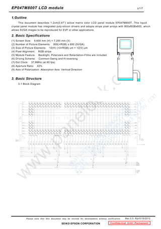
  • 1. This document describes 1.2cm(0.47”) active matrix color LCD panel module EP047M800T. This liquid EP047M800T LCD module p1/7 P l e a s e n o t e t h a t t h i s d o c u m e n t m a y b e r e v i s e d f o r d e v e l o p m e n t w i t h o u t n o t i f i c a t i o n . Rev.0.5 April/15/2013 SEIKO EPSON CORPORATION Confidential Until Permanent 1.Outline crystal panel module has integrated poly-silicon drivers and adopts stripe pixel arrays with 800xRGBx600, which allows SVGA images to be reproduced for EVF or other applications. 2. Basic Specifications (1) Screen Size: 9.600 mm (H) × 7.200 mm (V) (2) Number of Picture Elements: 800(×RGB) x 600 (SVGA) (3) Size of Picture Elements: 12(H) (=4×RGB) um × 12(V) um (4) Pixel Alignment: RGB stripe (5) Module Feature: Backlight, Polarizers and Retardation-Films are included (6) Driving Scheme: Common-Swing and H-reversing (7) Dot Clock: 37.8MHz (at 60 fps) (8) Aperture Ratio: 42% (9) Axis of Polarization: Absorption Axis: Vertical Direction 3. Basic Structure 3.1 Block Diagram w h a t s a p p :   + 8 6   1 8 5 6 6 2 9 4 2 1 8 S k y p e :   p a n o x s h a w n @ o u t l o o k . c o m E m a i l :   s h a w n . l e e @ p a n o x d i s p l a y . c o m
  • 2. p2/7 P l e a s e n o t e t h a t t h i s d o c u m e n t m a y b e r e v i s e d f o r d e v e l o p m e n t w i t h o u t n o t i f i c a t i o n . Rev.0.5 April/15/2013 SEIKO EPSON CORPORATION Confidential Until Permanent 㩷 3.2 Input Pin Description (Panel) No. Name No. Name No. Name No. Name 1 LCCOM 14 DX 27 VID-R12 40 VID-B1 2 VSSY 15 VSSX 28 VID-G1 41 VID-B2 3 DY 16 VID-R1 29 VID-G2 42 VID-B3 4 CLY 17 VID-R2 30 VID-G3 43 VID-B4 5 ENBY 18 VID-R3 31 VID-G4 44 VID-B5 6 DIRY 19 VID-R4 32 VID-G5 45 VID-B6 7 VDD 20 VID-R5 33 VID-G6 46 VID-B7 8 NRG 21 VID-R6 34 VID-G7 47 VID-B8 9 ENBX1 22 VID-R7 35 VID-G8 48 VID-B9 10 ENBX2 23 VID-R8 36 VID-G9 49 VID-B10 11 ENBX3 24 VID-R9 37 VID-G10 50 VID-B11 12 ENBX4 25 VID-R10 38 VID-G11 51 VID-B12 13 CLX 26 VID-R11 39 VID-G12 3.3 Input Pin Description (LED Backlight) No. Name 1 BLC 2 BLC 3 BLA 4 BLA 3.4 Input Pin Number Description Notation Function DX Start Pulse Input of X Shift Register, which is part of the X Driver CLX Input of X Shift Register for the Transfer Clock, which is part of the X Driver ENBX1㨪4 Enable signal inputs for X Shift Register VID-R/G/B1㨪12 Video Signal and Video Noise Reduction Inputs DY Start Pulse Input of Y Shift Register, which is part of the Y Driver CLY Input of Y Shift Register for the Transfer Clock, which is part of the Y Driver ENBY Enable Signal Input for Y Shift Register DIRY Scan Direction Select Input of Y Driver; DIRY=L: Down Shift, DIRY=H: Up Shift NRG Enable Signal Input for Video Noise Reduction LCCOM Input of Opposite Electrode of Liquid Crystal Panel VDD Positive Supply Voltage Input for X Driver and Y Driver 㨄 VSSX Negative Supply Voltage Input for X Driver VSSY Negative Supply Voltage Input for Y Driver BLC Power Supply Input for Backlight (Cathode) BLA Power Supply Input for Backlight (Anode) EP047M800T LCD module w h a t s a p p :   + 8 6   1 8 5 6 6 2 9 4 2 1 8 S k y p e :   p a n o x s h a w n @ o u t l o o k . c o m E m a i l :   s h a w n . l e e @ p a n o x d i s p l a y . c o m
  • 3. p3/7 P l e a s e n o t e t h a t t h i s d o c u m e n t m a y b e r e v i s e d f o r d e v e l o p m e n t w i t h o u t n o t i f i c a t i o n . Rev.0.5 April/15/2013 SEIKO EPSON CORPORATION Confidential Until Permanent 4. Maximum Ratings Item Notation Rated Value Unit Supply Voltage for X driver VDD㧙VSSX -1.0 㨪 +20.0 V Supply Voltage for Y driver VDD㧙VSSY -1.0 㨪 +20.0 V Back Bias VSSY㧙VSSX -5.0 㨪 -2.0 V Voltage of X Driver Input Terminal VIX㧙VSSX -1.0 㨪 VDD+1.0 V Voltage of Y Driver Input Terminal VIY㧙VSSY -1.0 㨪 VDD+1.0 V Forward DC Current of LED Backlight (25ºC) IBL 35 mA Storage Temperature Range Tstg -30~+80 ºC 5. Standard Operation 㩷 㩷 㩷 㩷 㩷 㩷 㩷 㩷 㩷 㩷 㩷 㩷 㩷 5.1 Standard Operation for Panel Item Notation Min. Typ. Max. Unit Supply Voltage for X Driver VDD㧙VSSX 10.0 11.0 12.0 V Supply Voltage for Y Driver VDD㧙VSSY 14.0 15.0 16.0 V Back Bias VSSY㧙VSSX 㧙 -4.0 㧙 V Low-level Voltage of X Driver Inputs DX , CLX, ENBX1㨪4 , NRG VIXL VSSX VSSX+0.4 V High-level Voltage of X Driver Inputs VIXH VDD-0.4 VDD V Low-level Voltage of Y Driver Inputs DY , CLY, DIRY ,ENBY VIYL VSSY VSSY+0.4 V High-level Voltage of Y Driver VIYH VDD-0.4 VDD V Center Voltage of Video Signal Input VVC 2.5 2.6 2.7 V Voltage Range of Video Signal Input VIDR/G/B1..12 VVC±2.5 V High-level Voltage of NRS VNRSH VVC V Low-level Voltage of NRS VNRSL VVC V Center Voltage of Opposite Electrode VCC 1.75 1.82 1.89 V Voltage Range of Opposite Electrode LCCOM VCC±2.5 V Operation Temperature Range 1) Top -10 70 ºC Note1: Not all characteristics in the panel can be guaranteed in this temperature range. 5.2 Standard Operation for Backlight Item Notation Min. Typ. Max. Unit LED Backlight DC Current (25 㧕 IBL 8.9 35 mA LED Backlight DC Voltage (25 㧕 VBL 3.5 V Note2: The numerical values described in Standard Operation are subject to change. EP047M800T LCD module w h a t s a p p :   + 8 6   1 8 5 6 6 2 9 4 2 1 8 S k y p e :   p a n o x s h a w n @ o u t l o o k . c o m E m a i l :   s h a w n . l e e @ p a n o x d i s p l a y . c o m
  • 4. p4/7 P l e a s e n o t e t h a t t h i s d o c u m e n t m a y b e r e v i s e d f o r d e v e l o p m e n t w i t h o u t n o t i f i c a t i o n . Rev.0.5 April/15/2013 SEIKO EPSON CORPORATION Confidential Until Permanent 6. Input Signal Timing㧔Ta = 0~70͠, Dot Clock 37.8MHz, CLX=0.79MHz, CLY=18.75kHz㧕 Item Notation Min. Typ. Max. Unit Timing Chart DX㧘NRG Rise, Fall Time tr㧘tf 50 ns DY Rise, Fall Time tr㧘tf 50 ns ENBX 1㨪4 Rise, Fall Time tr㧘tf 50 ns ENBY 1㧘2 Rise Fall Time tr㧘tf 50 ns CLX Rise Time trCLX 50 ns CLX Fall Time tfCLX 50 ns CLY Rise Time trCLY 100 ns CLY Fall Time tfCLY 100 ns DX Data Set-up Time tDSX 635 ns DX Data Hold Time tDHX 635 ns CLX Fall Time ĺ DX Rise tCLXDX 1.518 ȝs DY Data Set-up Time tDSY 26.5 ȝs DY Data Hold Time tDHY 26.5 ȝs CLY Fall Time ĺ DY Rise Time tCLYDY 503.2 ȝs Horizontal Blanking Period tH 4.9 ȝs VID Disp. End ĺ ENBY Fall 3) tpHLENBY 705 805 905 ns ENBY Fall ĺ VID Polarity Inversion tpLHENBY 1494 1549 1694 ns CLY Rise ĺ VID Polarity Inversion tpCLY -50 0 ns ENBY Rise ĺ NRG Rise tpNRG 0 100 200 ns NRS Insert Starting Point ĺNRG Rise tpLHNRG 0 80 180 ns Pulse Width of NRG tpwNRG 628 728 828 ns NRS Insert Period 4) tpNRS 1020 ns NRG Fall ĺ DX Rise tpDX 244 344 444 ns NRG Fall ĺ VID Start 5) tpstVID 1285 ns EBX2 Fall ĺ CLX Rise Time tDSEBX2 288 ns EBXn Fall ĺEBXn+1 Fall tpdEnEn+1 313 318 323 ns Pulse Width 0f EBX1-4 tpwEBX 171 176 181 ns ENBY Fall ĺ CLY tpLENBY 1540 1640 1740 ns CLY ĺ ENBY Rise tpHENBY 220 320 420 ns ENBY Pulse Interval tpdENBY 1.9 ȝs CLY ĺ LCCOM tCLYCOM 0 ȝs Note3: This describes the VID end for Active Display Area and the timing of the last VID-R/G/B1~4 input to Active Display Area. Note4: This cannot be checked in the waveforms from the driver IC:L3E03100F0A because there is a high impedance period after/before NRS inserting period. This describes a timing set in our register. Note5: This describes the VID start for Active Display Area and the timing of the first VID-R/G/B1~4 input to Active Display Area. 㪚㪣㪰 㪛㪰 㫋㪛㪟㪰 㪌㪇㩼 㫋㪚㪣㪰㪛㪰 㪌㪇㩼 㪌㪇㩼 㫋㪛㪪㪰 㪌㪇㩼 㪚㪣㪯 㪛㪯 㪌㪇㩼 㪌㪇㩼 㪌㪇㩼 㪌㪇㩼 㫋㪚㪣㪯㪛㪯 㫋㪛㪪㪯 㫋㪛㪟㪯 㪐㪇㩼 㫋㫉㪚㪣 㪐㪇㩼 㪈㪇㩼 㪈㪇㩼 㫋㪽㪚㪣 㫋㫉 㫋㪽 㪐㪇㩼 㪈㪇㩼 㪐㪇㩼 㪈㪇㩼 㫋㫇㫊㫋㪭㪠㪛 㪭㪥㪩㪪㪟㪆㪣 㪌㪇㩼 㪌㪇㩼 㪌㪇㩼 㪌㪇㩼 㪌㪇㩼 㪌㪇㩼 㪛㪯 㪥㪩㪞 㪚㪣㪰 㪜㪥㪙㪰 㪌㪇㩼 㪌㪇㩼 㫋㫇HLENBY 㫋㫇㪚㪣㪰 㫋㫇㪣㪟㪥㪩㪞 㫋㫇㪛㪯 㫋㫇㫎㪥㪩㪞 ᳓ᐔᏫ✢ᦼ㑆 㫋㫇LHENBY 㫋㫇㪥㪩㪞 㪭㪠㪛㪄㪩㪆㪞㪆㪙 䵾 䵾 䵾 䵾 㪈 亖 㪈㪉 㪌㪇㩼 㫋㫇㪥㪩㪪 Horizontal Blanking Period 㪣㪚㪚㪦㪤 㫋㫇㪟㪜㪥㪙㪰 㫋㫇㪣㪜㪥㪙㪰 㪌㪇㩼 㪌㪇㩼 㪌㪇㩼 㪌㪇㩼 㪚㪣㪰 㪜㪥㪙㪰 㪭㪠㪛 㪌㪇㩼 㪌㪇㩼 㫋㫇㪻㪣㪜㪥㪙㪰 㫋㫇㪁㪁㪁㪁 㪜㪙㪯㪉 㪜㪙㪯㪋 㪜㪙㪯㪊 㪜㪙㪯㪈 㪚㪣㪯 㪌㪇㩼 㪌㪇㩼 㪌㪇㩼 㪌㪇㩼 㪌㪇㩼 㪌㪇㩼 㪌㪇㩼 㪌㪇㩼 㪌㪇㩼 㪌㪇㩼 㫋㪛㪪㪜㪙㪯㪉 㫋㫇㪻㪜㫅㪜㫅㪂㪈㫋㫇㪻㪜㫅㪜㫅㪂㪈 㫋㫇㪻㪜㫅㪜㫅㪂㪈 㫋㫇㪻㪜㫅㪜㫅㪂㪈 㫋㫇㫎㪜㪙㪯 㫋㫇㫎㪜㪙㪯 㫋㫇㫎㪜㪙㪯 㫋㫇㫎㪜㪙㪯 EP047M800T LCD module w h a t s a p p :   + 8 6   1 8 5 6 6 2 9 4 2 1 8 S k y p e :   p a n o x s h a w n @ o u t l o o k . c o m E m a i l :   s h a w n . l e e @ p a n o x d i s p l a y . c o m
  • 5. p5/7 P l e a s e n o t e t h a t t h i s d o c u m e n t m a y b e r e v i s e d f o r d e v e l o p m e n t w i t h o u t n o t i f i c a t i o n . Rev.0.5 April/15/2013 SEIKO EPSON CORPORATION Confidential Until Permanent 7. Electrical Characteristics VDD㧙VSSX=11.0V‫ޔ‬VDD㧙VSSY=15.0V X Driver Item Symbol Min. Typ. Max. Unit Condition Clock Input Terminal Capacitance 㧯 CLX 7.9 pF f=100KHz Start-Pulse Input Terminal Capacitance 㧯 DX 5.2 pF Video Input Terminal Capacitance R,G, B 㧯 VR 㧯 VG 㧯 VB 15 13 17 pF ENBX Input Terminal Capacitance 㧯 ENBX 8.0 pF NRG Input Terminal Capacitance 㧯 ENB 9.7 pF Y Driver Item Symbol Min. Typ. Max. Unit Condition Clock Input Terminal Capacitance 㧯 CLY 17.5 pF f=100KHz Start-Pulse Input Terminal Capacitance 㧯 DY 26.6 pF DIRY Input Terminal Capacitance 㧯 DIRY 17.9 pF ENBY Input Terminal Capacitance 㧯 ENBY 113.8 pF Panel Current Consumption 6) Item Symbol Min. Typ. Max. Unit Condition Panel Current Consumption 㧼 0.7 1.0 mA Panel Power Consumption 7) Item Symbol Min. Typ. Max. Unit Condition Panel Power Consumption 㧼 7.2 11.5 mW Backlight Power Consumption 26 mW Note6,7: Panel Current/Power Consumption in integrated drivers are described except for the consumption of VID and LCCOM. EP047M800T LCD module w h a t s a p p :   + 8 6   1 8 5 6 6 2 9 4 2 1 8 S k y p e :   p a n o x s h a w n @ o u t l o o k . c o m E m a i l :   s h a w n . l e e @ p a n o x d i s p l a y . c o m
  • 6. p6/7 P l e a s e n o t e t h a t t h i s d o c u m e n t m a y b e r e v i s e d f o r d e v e l o p m e n t w i t h o u t n o t i f i c a t i o n . Rev.0.5 April/15/2013 SEIKO EPSON CORPORATION Confidential Until Permanent 8. Optical Characteristics Standard Item Symbol Min. Typ. Max. Unit Condition Contrast Ratio 25͠ CR 1:180 1:280 㧙 [1] V90(25) 0.85 1.15 1.45 V50(25) 1.43 1.73 2.03 Voltage-Transmittance Characteristic 25͠ V10(25) 2.12 2.42 2.72 V [2] 25͠ ton(25) 3 Response Time toff(25) 10 msec [3] Flicker 25͠ F -26 dB [4] Brightness 25͠ 250 460 nit [5] Color Temperature W 5000 7100 9800 K 䌸㩷 㪉㪌㷄㩷 㪮㫏㩷 㩷 0.300 㩷 㪮㩷 䌹㩷 㪉㪌㷄㩷 㪮㫐㩷 㩷 0.311 㩷 䋭㩷 䌸㩷 㪉㪌㷄㩷 㪩㫏㩷 0.578 0.618 0.658 㪩㩷 䌹㩷 㪉㪌㷄㩷 㪩㫐㩷 0.301 0.341 0.381 䋭㩷 䌸㩷 㪉㪌㷄㩷 㪞㫏㩷 0.266 0.306 0.346 㪞㩷 䌹㩷 㪉㪌㷄㩷 㪞㫐㩷 0.574 0.614 0.654 䋭㩷 䌸㩷 㪉㪌㷄㩷 㪙㫏㩷 0.112 0.152 0.192 Chroma- ticity㩷 㩷 㪙㩷 䌹㩷 㪉㪌㷄㩷 㪙㫐㩷 0.019 0.059 0.099 䋭㩷 [6] Color Gamut (NTSC Ratio) 60 65 % [7] EP047M800T LCD module w h a t s a p p :   + 8 6   1 8 5 6 6 2 9 4 2 1 8 S k y p e :   p a n o x s h a w n @ o u t l o o k . c o m E m a i l :   s h a w n . l e e @ p a n o x d i s p l a y . c o m
  • 7. p7/7 P l e a s e n o t e t h a t t h i s d o c u m e n t m a y b e r e v i s e d f o r d e v e l o p m e n t w i t h o u t n o t i f i c a t i o n . Rev.0.5 April/15/2013 SEIKO EPSON CORPORATION Confidential Until Permanent Condition of Measurement for Optical Characteristics (1) In the condition 1, 5, 6, and 7, these are measured with SR-3AR in room temperature. Attachment Lens AL-6 is used. Detection angle is 2º. These are the characteristics from the vertical direction. (2) In the condition 2 and 3, these are the characteristics from the vertical direction (These are measured with straight ray guided by optical fiber as a light source of Halogen Lamp.) (3) In the condition 4, Flicker is measured at room temperature from the vertical direction with FFT analyzer that can transform in frequency component. (4) 5. Standard Operation and 6 input signal timing are used in the circuit condition. LCCOM is set to be optimum. Condition 1: The center of the display area is measured. L(White, Video voltage 0V) CR= L(Black, Video voltage 5V) Condition 2: The center of the display area is measured. In Fig. a, Normalized Transmittance is defined as 100% when input voltages are given 0V. V90, V50 and V10 represent the voltages at which the transmittance is 90%, 50% and 10%, respectively. Condition 3: The center of the display area is measured. When the video voltage is 0V, the transmittance is defined as 100% Ton represents the optical response time at 10% of the transmittance while the video voltage is changing from 0V to 5V. Toff represents the optical response time at 90% of the transmittance while the video voltage is changing from 5V to 0V. Condition 4: Flicker is measured on a stripe pattern image where black lines (Video voltage 5V) and gray lines (Video voltage 2V) are displayed on every other line. 30Hz Component F = 20 ×log DC Component Condition 5: Brightness is measured at the center of the display area while white image is being displayed. Condition 6: Color Temperature and Chromaticity are measured at the center of the display area while each of white, R, G, and B images is being displayed. Condition 7: Each mono-color image of RGB is measured at the center of the display area. The area that consists of the measured color gamut points is compared with that of NTSC. ࿑㨍ࡄࡀ࡞ࠦࡦ࠻࡜ࠬ࠻ࠞ࡯ࡉ 0% 25% 50% 75% 100% 0.0 1.0 2.0 3.0 4.0 5.0 ࡄࡀ࡞ࡆ࠺ࠝ┵ሶ߳ߩශട㔚࿶=8? ⷙᩰൻㅘㆊ₸ 90 50 10 V(90) V(50) V(10) Normalized Transmittance Applied Voltage at Video Terminals Fig. a㨫 V-T Curve EP047M800T LCD module w h a t s a p p :   + 8 6   1 8 5 6 6 2 9 4 2 1 8 S k y p e :   p a n o x s h a w n @ o u t l o o k . c o m E m a i l :   s h a w n . l e e @ p a n o x d i s p l a y . c o m
  • 8. p8/7 P l e a s e n o t e t h a t t h i s d o c u m e n t m a y b e r e v i s e d f o r d e v e l o p m e n t w i t h o u t n o t i f i c a t i o n . Rev.0.5 April/15/2013 SEIKO EPSON CORPORATION Confidential Until Permanent 9. Reliability Test Test Item Test Method Judgement Criterion 㧝 High Temperature Storage 240 hours storage at 80±2ºC 㧞 High Temperature Operation 240 hours normal* operation at 70±2ºC 㧟 Low Temperature Storage 240 hours storage at -30±2ºC 㧠 High Temperature High Humidity Operation 240 hours normal* operation at 40ºC, 90㧑 㧡 Temperature Cycle -30ºC = 20 ~ 25ºC = 80ºC, 10 cycles (1H) (1H) (1H) 㧢 Static Electricity 100pF㧘1.5kȍ㧘100V 20~25ºC㧘60ºC RH For normal use, major abnormality shall not be found in terms of display/panel appearance. Note: Tests shall be conducted after samples have been left at room temperature for 4 hours. 㧣 Vibration 10㨪55Hz‫ޔ‬1 minute cycle, Amplitude of 1.5mm, for 20 minutes in each of X, Y, and Z directions. 㧤 Package Drop Test in accordance with JIS Z-0202. Drop hight is 70±5cm for Plane, 40±5cm for Corner and Edge. The number of test times is one. 㧥 Shock 490m/sec 2 (50G), once in each of X,Y, and Z directions. For normal use, major abnormality shall not be found in terms of display/panel appearance. *A gray levell (middle) voltage is applied for Video Signals. The value and frequency are decided separately. 10. Outline Image Hook Black Mask Panel Polarizer Cover Glass Substrate Counter Substrate Frame Backlight Hook Mask Polarizer Backlight 㩷 EP047M800T LCD module w h a t s a p p :   + 8 6   1 8 5 6 6 2 9 4 2 1 8 S k y p e :   p a n o x s h a w n @ o u t l o o k . c o m E m a i l :   s h a w n . l e e @ p a n o x d i s p l a y . c o m