1.39 inch Round OLED 454X454 SPI/MIPI
•
0 likes•10 views

Display Type AM-OLED Display Brand BOE Interface SPI,MIPI Screen Size 1.39 inch Orientation Landscape Display Color Full Color Manufacturer BOE Resolution 454x454 Driver IC RM69330 Consumption 50uW~260mW Active Area (mm) ¢35.412 Luminance 800 cd/m2 (Max) Viewing Angle 80/80/80/80 (Typ.)(CR≥10) Color Depth 16.7M Refresh Rate 45 Hz For More Display Photo https://www.panoxdisplay.com/amoled/1-39-inch-round-oled-454x454-spi.html

Recommended
More Related Content
Similar to 1.39 inch Round OLED 454X454 SPI/MIPI
Similar to 1.39 inch Round OLED 454X454 SPI/MIPI (20)
More from Panox Display
More from Panox Display (12)
Recently uploaded
Recently uploaded (20)
1.39 inch Round OLED 454X454 SPI/MIPI
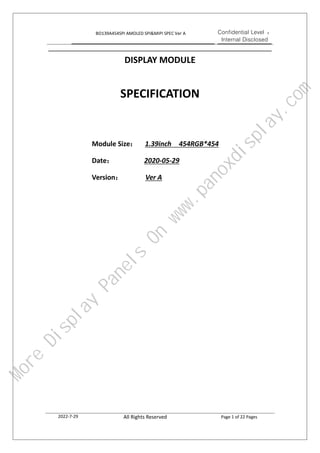
- 1. BO139A454SPI AMOLED SPI&MIPI SPEC Ver A Confidential Level : Internal Disclosed 2022-7-29 All Rights Reserved Page 1 of 22 Pages DISPLAY MODULE SPECIFICATION Module Size: 1.39inch 454RGB*454 Date: 2020-05-29 Version: Ver A M o r e D i s p l a y P a n e l s O n w w w . p a n o x d i s p l a y . c o m
- 2. BO139A454SPI AMOLED SPI&MIPI SPEC Ver A Confidential Level : Internal Disclosed 2022-7-29 All Rights Reserved Page 2 of 22 Pages All rights reserved Revision History Version Revise Date Page Content Prepared by Table of Contents 1 General Specification................................................................................................................. 3 1.1 Features...........................................................................................................................3 1.2 Application..................................................................................................................... 3 1.3 General Specification..................................................................................................... 3 2 Pin Assignments......................................................................................................................... 5 3 Schematic Circuit Diagram........................................................................................................ 6 3.1 MIPI Reference Circuit.................................................................................................. 6 4 Register &Pixel Data Format..................................................................................................... 8 4.1 MIPI 24 bit Data Format................................................................................................ 8 4.2 Graphic memory writing direction.................................................................................7 5 Timing Characteristics................................................................................................................8 5.1 MIPI Interface Characteristics....................................................................................... 8 6 Electrical Specifications........................................................................................................... 11 6.1 DC Characteristics Requirements.............................................................................. 112 6.2 Power Consumption of Panel.......................................................................................11 7 Optical Specifications...............................................................................................................12 8 Mechanical Drawing................................................................................................................ 21 9 Reliability Requirement............................................................................................................22 9.1 General Reliability Requirement..................................................................................22 9.2 Incoming Inspection Requirement...............................................错误!未定义书签。 9.3 Module Unit Reliability Test....................................................... 错误!未定义书签。 M o r e D i s p l a y P a n e l s O n w w w . p a n o x d i s p l a y . c o m
- 3. BO139A454SPI AMOLED SPI&MIPI SPEC Ver A Confidential Level : Internal Disclosed 2022-7-29 All Rights Reserved Page 3 of 22 Pages 1 General Specification 1.1 Features General Specification-- AMOLED --MIPI --COF -- Board to Board Connection --Outline & AA are round 1.2 Application Display terminals for Round Watch. 1.3 General Specification Table 1 General Specification No. Item Specification Unit Remark 1 Display Size 1.39 Inch 2 Array Technology Type LTPS 3 Display Type AMOLED 4 Resolution 454RGB*454(Real RGB or equivalent ) 5 Color Depth 16.7M 6 Viewing Direction All direction Note 1 7 Contrast Ratio 100000:1 Min 8 Luminance 450cd/m2 cd/m 2 Typ 9 Panel Size 39.41(H)+39.61(V)+0.654(T) Mm Note 1 10 Panel Maximum Thickness 0.733(MDL) Mm Note 1 11 Module Outline <=φ42 Mm Include COF bending dimension 12 Panel Active Area ¢35.412 Mm Diameter M o r e D i s p l a y P a n e l s O n w w w . p a n o x d i s p l a y . c o m
- 4. BO139A454SPI AMOLED SPI&MIPI SPEC Ver A Confidential Level : Internal Disclosed 2022-7-29 All Rights Reserved Page 4 of 22 Pages 13 Pixel Size 78*78 Μm 14 Pixel Pitch 78 Μm 15 Pixel Aspect Ratio 1:1 16 Driver IC RM69330 17 Driver IC RAM Size Full RAM or1/2 RAM 18 Light Source OLED 19 Interface MIPI/SPI 20 Operation Temperature -20~70 degC 21 Storage Temperature -30~80 degC 22 Weight 2.48(MDL) Gram ±15% 23 Pixel Per Inch 326 PPI 24 Environmental Protection Requirement RoHS & REACH must be executed 25 Connection Method BM28U-24DP/2-0.35V(86) 26 Gamma Correction R/G/B separation 27 Polarizer Type Hard coat treating 3H Glare 28 Panel gate scan direction Pad to pad Opposite Note 2 29 Warpage Front side warpage value < 0.1mm;Rear side warpage value(w/o foam) < 0.1mm Note 3 30 GSM TDMA Noise Input support 500mV drop Note4 31 Antenna Interference AMOLED can not interference Antenna Note1:Please Refer to the mechanical drawing. Note2:Some GOP panel can not support gate bidirectional scanning , or even some gate bidirectional scanning GOP panel are abnormal working when the gate scanning direction set to be reversed. Note3: Warpage inspected by Manual height/ flatness test instrument.(4 points position is defined Note4: TDMA Frame(4.615ms)Includes 8 time slots(1 time slot=577us) ,1 TDMA Frame has 1 time slot 577us drop 500mV, AMOLED can not display abnormal. M o r e D i s p l a y P a n e l s O n w w w . p a n o x d i s p l a y . c o m
- 5. BO139A454SPI AMOLED SPI&MIPI SPEC Ver A Confidential Level : Internal Disclosed 2022-7-29 All Rights Reserved Page 5 of 22 Pages Fig 1 TDMA Frame 2 Pin Assignments Table 2 PIN Assignments Pin No. Symbol I/O Function 1 XRES I Device reset signal (0 : enable ; 1 : Disable) 2 VCI_EN I VCI enable signal 3 NC(MTP) - Floating 4 GND Power Ground 5 TE O Synchronous signal output from panel to avoid tearing effect 6 DSI_D0N I/O MIPI data negative signal 7 AM_SPI_CSX I SPI interface 8 DSI_D0P I/O MIPI data positive signal 9 AM_SPI_SCL I SPI interface 10 GND Power Ground 11 AM_SPI_DCX I SPI interface 12 DSI_CLKN I MIPI strobe negative signal 13 AM_SPI_SDI I/O SPI interface 14 DSI_CLKP I MIPI strobe positive signal 15 AM_SPI_SDO I/O SPI interface 16 GND Power Ground 17 NC - Floating 18 VDDIO Power Power supply for interface system except MIPI interface 19 VBAT Power AMOLED power 20 VDDIO Power Power supply for interface system except MIPI interface 21 VBAT Power AMOLED power 22 VBAT Power AMOLED power 23 VBAT Power AMOLED power 24 VBAT Power AMOLED power Note ID: This pin definition needs to confirm with hardware engineer before AMOLED FPC fixed. M o r e D i s p l a y P a n e l s O n w w w . p a n o x d i s p l a y . c o m
- 6. BO139A454SPI AMOLED SPI&MIPI SPEC Ver A Confidential Level : Internal Disclosed 2022-7-29 All Rights Reserved Page 6 of 22 Pages 3 Schematic Circuit Diagram 3.1 MIPI Reference Circuit Fig 2 MIPI Reference Circuit M o r e D i s p l a y P a n e l s O n w w w . p a n o x d i s p l a y . c o m
- 7. BO139A454SPI AMOLED SPI&MIPI SPEC Ver A Confidential Level : Internal Disclosed 2022-7-29 All Rights Reserved Page 7 of 22 Pages 4 Register &Pixel Data Format 4.1 MIPI 24 bit Data Format Fig3 MIPI 24 Bit Data Format 4.2 Graphic memory writing direction Fig 4 Graphic Memory Writing Direction M o r e D i s p l a y P a n e l s O n w w w . p a n o x d i s p l a y . c o m
- 8. BO139A454SPI AMOLED SPI&MIPI SPEC Ver A Confidential Level : Internal Disclosed 2022-7-29 All Rights Reserved Page 8 of 22 Pages 5 Timing Characteristics 5.1 MIPI Interface Characteristics Fig 5 MIPI Interface Characteristics M o r e D i s p l a y P a n e l s O n w w w . p a n o x d i s p l a y . c o m
- 9. BO139A454SPI AMOLED SPI&MIPI SPEC Ver A Confidential Level : Internal Disclosed 2022-7-29 All Rights Reserved Page 9 of 22 Pages M o r e D i s p l a y P a n e l s O n w w w . p a n o x d i s p l a y . c o m
- 10. BO139A454SPI AMOLED SPI&MIPI SPEC Ver A Confidential Level : Internal Disclosed 2022-7-29 All Rights Reserved Page 10 of 22 Pages M o r e D i s p l a y P a n e l s O n w w w . p a n o x d i s p l a y . c o m
- 11. BO139A454SPI AMOLED SPI&MIPI SPEC Ver A Confidential Level : Internal Disclosed 2022-7-29 All Rights Reserved Page 11 of 22 Pages 6 Electrical Specifications 6.1 DC Characteristics Requirements Table 3 DC Characteristics Requirements Item Symbol Values Unit Remark Min Typ Max I/O Supply Voltage VDDIO 1.65 1.8 1.95 V Battery power Voltage Vbat 2.9 3.7 4.8 V Input High Voltage VIH 0.8*VDDIO -- VDDIO V Input Low Voltage VIL 0 -- 0.2*VDDIO V Output High Voltage VOH 0.8*VDDIO -- VDDIO V Output Low Voltage VOL 0 -- 0.2*VDDIO V Frame Frequency1 FFRAME 43 45 47 HZ 6.2 Power Consumption of Panel Power Supply: VDDIO=1.8V Vbat=3.7V Table 4 Power Consumption of Panel Display Mode Item Typ Max Remark Power (mW) Power (mW) 100% Pixel On,450nits,45Hz Normal mode 260 All Pixel Off,0nits,45Hz Normal mode 38 All Pixel Off,0nits/Vci on/Vddio on Standby mode 1.2 All Pixel Off,0nits/ Vci off/Vddio on Standby mode <50μW 10% Pixel On,50nits,15Hz Idle mode TBD 100% Pixel On,800nits,45Hz Boost mode TBD Note: Selecting different display mode supported by software setting. M o r e D i s p l a y P a n e l s O n w w w . p a n o x d i s p l a y . c o m
- 12. BO139A454SPI AMOLED SPI&MIPI SPEC Ver A Confidential Level : Internal Disclosed 2022-7-29 All Rights Reserved Page 12 of 22 Pages 7 Optical Specifications Test condition:VDDIO=1.8V , Vbat=3.7V ,Ta=25℃ Table 5 Optical Specifications Item Symbol Condition Min Typ Max Unit Note Luminance Bp θ=0° ɸ=0° TBD 450 TBD cd/m2 CPK>1.3 3 Note8 Boost Bp θ=0° ɸ=0° TBD 800 TBD cd/m2 Uniformity △Bp 85 -- -- % Note9 Viewing Angle2 Left θL Cr≥10 80 -- -- deg Note 10 Right θR 80 -- -- Top ψT 80 -- -- Botto m ψB 80 -- -- Contrast Ratio Cr θ=0° ɸ=0° 100000:1 -- - Note 11 Response Time Tr -- 2 3 ms Note 12 Tf -- 2 3 ms Tgray - 2 3 ms Color Coordinat e of CIE1931 Red x θ=0° ɸ=0° 0.64 0.67 0.70 - Note 13 y 0.290 0.329 0.350 Green x 0.186 0.226 0.266 y 0.675 0.715 0.755 Blue x 0.123 0.138 0.163 y 0.035 0.055 0.075 White x 0.28 0.3 0.32 y 0.29 0.31 0.33 NTSC Ratio NTSC CIE1931 85 100 -- % Note 14 Flicker amount - - -- -30 dB Note 15 Gamma - - 1.9 2.2 2.5 Note 16 Crosstalk △CT - - -- 1.1 Note 17 Reflectance Rf @550nm -- TBD -- % Note 18 Polarization direction of front polarizer PdF -- 135 -- deg Note 19 Luminance decrease ratio of full white θL=30° 35 40 % Note 20 θR=30° 35 40 % ψT=30° 35 40 % ψB=30° 35 40 % M o r e D i s p l a y P a n e l s O n w w w . p a n o x d i s p l a y . c o m
- 13. BO139A454SPI AMOLED SPI&MIPI SPEC Ver A Confidential Level : Internal Disclosed 2022-7-29 All Rights Reserved Page 13 of 22 Pages Color Shift θL=30° --- 5 JNCD Note 21 θR=30° --- 5 JNCD ψT=30° -- 5 JNCD ψB=30° -- 5 JNCD OLED lifetime 1.39* (TYP brightn ess) At25℃,wit h white color pattern 150 hrs Image sticking With 8*8 black-white chess board test image, lighting on with maximum luminance for 12H Light off or gray display for 3 minutes, normal performanc e after the test, without image sticking. Level 1(450nit, 127) White color uniformity B 标: Max △u'v'-A ≤0.014; Max △u'v'-B) ≤0.007 Note 22 Note 8: Luminance measurement The test condition is at 25℃ and measured on the surface of OLED module. The data are measured after OLEDs are lighted on for more than 5 minutes and displays are fully white. The brightness is the average value of 5 measured spots. Measurement equipment CS2000 or similar equipments (Field of view:1deg,Distance:50cm) • Measuring surroundings: Dark room. • Measuring temperature: Ta=25℃. • Adjust operating voltage to get optimum contrast at the center of the display. • Measured value at the center point of panel must be after more than 5 minutes while backlight turning on. M o r e D i s p l a y P a n e l s O n w w w . p a n o x d i s p l a y . c o m
- 14. BO139A454SPI AMOLED SPI&MIPI SPEC Ver A Confidential Level : Internal Disclosed 2022-7-29 All Rights Reserved Page 14 of 22 Pages Note 9: Uniformity • The test condition is at 25℃ and measured on the surface of display module. • Measurement equipment: CS2000 or similar equipments. • The luminance uniformity is calculated by using following formula: • △Bp = Bp (Min.) / Bp (Max.)×100 (%) • Bp (Max.) = Maximum brightness in 5 measured spots • Bp (Min.) = Minimum brightness in 5 measured spots. Note 10: The definition of Viewing Angle Refer to the graph below marked by θ and Ф M o r e D i s p l a y P a n e l s O n w w w . p a n o x d i s p l a y . c o m
- 15. BO139A454SPI AMOLED SPI&MIPI SPEC Ver A Confidential Level : Internal Disclosed 2022-7-29 All Rights Reserved Page 15 of 22 Pages Fig 6 The definition of Viewing Angle Note 11: The definition of Contrast Ratio (Test OLED using CS2000 or similar equipments): Luminance When OLED is at “White” state Contrast Ratio(CR)= Luminance When OLED is at “Black” state (Contrast Ratio is measured in optimum common electrode voltage. Black state display pure black color and luminance<0.003nits.) Note 12: Definition of Response time. (Test OLED using DMS501 or similar equipments): The output signals of photo detector are measured when the input signals are changed from “black” to “white”(Voltage falling time) and from “white” to “black”(Voltage rising time), respectively. The response time is defined as the time interval between the 10% and 90% of amplitudes. Refer to figure as below. M o r e D i s p l a y P a n e l s O n w w w . p a n o x d i s p l a y . c o m
- 16. BO139A454SPI AMOLED SPI&MIPI SPEC Ver A Confidential Level : Internal Disclosed 2022-7-29 All Rights Reserved Page 16 of 22 Pages Response time of gray to gray:(In 8 grays, neighboring gray-scale intensity can not capture, substitute with the brightness of the between level1 ~ level2) • Measurement equipment: DMS501 or similar equipments. • Test method :we define 8 grays L0-L7, the grays of L0-L7 were defined as:0,36,73, 109, 146, 182, 219, 255. The output signals of photo detector are measured when the input signals are changed from “Lx” to “Ly”, x, y= [0, 7]. The response time is defined as the time interval between the 10% and 90% of amplitudes. The result of the test can be noted as below: L0 L1 L2 L3 L4 L5 L6 L7 L0 L1 L2 L3 L4 L5 L6 L7 Note 13: Color Coordinates of CIE 1931 • The test condition is at 25℃ and measured on the surface of display module. • Measurement equipment: CS2000 or similar equipments. • The Color Coordinate (CIE 1931) is the measurement of the center of the display shown in below figure. Note 14: Definition of Color of CIE Coordinate and NTSC Ratio. 100% triangle NTSC of area triangle RGB of area S M o r e D i s p l a y P a n e l s O n w w w . p a n o x d i s p l a y . c o m
- 17. BO139A454SPI AMOLED SPI&MIPI SPEC Ver A Confidential Level : Internal Disclosed 2022-7-29 All Rights Reserved Page 17 of 22 Pages Note 15: Flicker • Measurement equipment :CA-210 or similar equipments • Measuring temperature: Ta=25℃. • Test method: JEITA method • Test pattern : Refer to below(Test Pattern should be full-fill of display screen) 1 L127 2 row 3 cloumn 4 white The point should be marked is, for line and frame inversion, the background of Flicker Test Pattern-“gray “ are defined as middle gray scale .For example, RGB 24bit “gray” defined as below: For Dot inversion, the RGB data for first pixel is (127, 0, 127), the RGB data for the second pixel is (0, 127, 0). • Frame Frequency Requirement:45HZ. • Measurement Point: the center of display active area. • Conversion of Flicker ratio: Flicker[dB] = 10xlog[Px/P0] Where Px: Maximum power spectrum of AC component after passing through integrator P0:Power spectrum of DC component after passing through integrator AC component=b (Refer to below diagram ) DC component=a (Refer to below diagram) M o r e D i s p l a y P a n e l s O n w w w . p a n o x d i s p l a y . c o m
- 18. BO139A454SPI AMOLED SPI&MIPI SPEC Ver A Confidential Level : Internal Disclosed 2022-7-29 All Rights Reserved Page 18 of 22 Pages Note 16: Gamma Curve Control • For gamma curve control, request as below: • 1,the whole curve’s tolerance must control within +/-0.3, will test the gray scale below: 0, 8, 16, 25, 33, 41, 49, 58, 66, 74, 82, 90, 99, 107, 115, 123, 132, 140, 148, 156, 165, 173, 181, 189, 197,206, 214, 222, 230, 239, 247, 255 Note 17: Crosstalk • There should be no visible cross-talk in normal direction of the display when the two ”Cross-talk Test Patterns ” below are loaded. • Measurement equipment: CS2000 or similar equipments • The point should be marked is, the background of Cross-talk Test Pattern-“gray “ are defined as middle gray scale . For example, RGB 24bit “gray” defined as below: • △Bpn = Bpn (gray) / Bpn (white) Which n means the dot No. In the Cross-talk Test Pattern ; Bpn (gray) means the brightness of the No.n spots in Cross-talk Test Pattern; Bpn (white) means the brightness of the No.n spots in Full white Test Pattern; • △Bp (Max.) = Maximum value in △Bp1~△Bp4. • △Bp (Min.) = Minimum value in △Bp1~△Bp4. • △CT=△Bp (Max.)/ △Bp(Min.). • △CT must be less than 1.10 M o r e D i s p l a y P a n e l s O n w w w . p a n o x d i s p l a y . c o m
- 19. BO139A454SPI AMOLED SPI&MIPI SPEC Ver A Confidential Level : Internal Disclosed 2022-7-29 All Rights Reserved Page 19 of 22 Pages Fig 7 Cross-talk Test Pattern Note 18:Reflectance Ratio • Measurement equipment : X-rite SP64 • Measurement parameter:Reflectance Ratio @550nm Note 19: Polarization Direction Definition • Viewing direction is normal user viewing direction which is vertical to the display surface • The polarizer which is closer to viewer is defined as Front Polarizer • The polarizer which is on the rear side of viewer is defined as Rear Polarizer • The X axis is defined as parallel line to top&bottom sidelines of the Active Area • PdF which is marked in blue arrow is polarization degree of Front polarizer • The polarization degree parameter must be indicated in range of 0deg to 180deg according to above definition • • Fig 8 Absorption axis Definition M o r e D i s p l a y P a n e l s O n w w w . p a n o x d i s p l a y . c o m
- 20. BO139A454SPI AMOLED SPI&MIPI SPEC Ver A Confidential Level : Internal Disclosed 2022-7-29 All Rights Reserved Page 20 of 22 Pages Note 20: Definition of Luminance Decrease Ratio • Refer to the graph of note 9. • Test pattern : Full White • The luminance decrease ratio is calculated by using following formula: Luminance test at θL/θR/ψT/ψB=30° Luminance decrease Ratio=1- Luminance test at θL/θR/ψT/ψB=0° Note 21: Color Shift JNCD • For JNCD measure: • Fix on one pattern like white pattern, • On the condition θ=0 F=0°, we can get the color coordinate (u1', v1') and onθL=30° we can get another color coordinate (u2', v2') • Delta = Square Root( (u2' - u1')^2 + (v2' - v1')^2 ) • JNCD stands for "Just Noticeable Color Difference" • For the (u', v') color space JNCD=0.0040. • 2JNCD means Delta u’v’<0.0080 • For color shift we need to measure white/red/green/blue pattern. • This Requirement is from our customer and we have test some of our phone display and the result is OK. Note 22: White Color Uniformity • The test condition is at 25℃ and measured on the surface of display module, The test location is same with uniformity • Measurement equipment: CS2000 or similar equipments. • The luminance uniformity is calculated by using following formula: • All measurements are color between any two points:△ u’v’-A=sqrt((um-un)2+(vm-vn) 2) • All measurements are color between any two adjacent points: △ u’v’-B=sqrt( (ui-uj) 2+ (vi-vj) 2) M o r e D i s p l a y P a n e l s O n w w w . p a n o x d i s p l a y . c o m
- 21. BO139A454SPI AMOLED SPI&MIPI SPEC Ver A Confidential Level : Internal Disclosed 2022-7-29 All Rights Reserved Page 21 of 22 Pages 8 Mechanical Drawing——PDF M o r e D i s p l a y P a n e l s O n w w w . p a n o x d i s p l a y . c o m
- 22. BO139A454SPI AMOLED SPI&MIPI SPEC Ver A Confidential Level : Internal Disclosed 2022-7-29 All Rights Reserved Page 22 of 22 Pages 9 Reliability Requirement 9.1 General Reliability Requirement Table 6 General Reliability Requirement Test item Test condition No. of failures /No. of examinations Vibration test Amplitude 1.5mm,f=10 to 55 Hz, 2 hours each in the X,Y and Z direction 0/3 Packing shock test Apply 1g for operation time 6ms, 3 times each in X,Y and Z direction 0/3 Packing vibration-proof test 2g, f=10->55->10Hz apply in each of X, Y, and Z direction for 30 min 0/3 Packing drop test Drop the packing from 75cm height, 3 times for 6-faces, 3-edges and 1-corner -- M o r e D i s p l a y P a n e l s O n w w w . p a n o x d i s p l a y . c o m