5.0 inch OLED 720x1280 MIPI Interface
•
0 likes•29 views

Model Name H497TLB01 Display Type AMOLED Display Brand AUO Interface MIPI Screen Size 5.0 Orientation Portrait Display Color Full Color Manufacturer AUO Resolution 720(RGB)×1280 Driver IC RM69052 Active Area (mm) 61.92(H)×110.08(V) mm Luminance 250 cd/m² (Typ.) Viewing Angle 80/80/80/80 (Min.)(CR≥200) Color Depth 16.7M 100% (CIE1931) Refresh Rate 60Hz Signal Type MIPI DSI,39 pin Voltage Supply Operating Temp -30 ~ 60 °C Storage Temp -40 ~ 70 °C Aspect Ratio 9:16 (H: V) Screen Type AM-OLED, OLED Arrangement RGB Vertical Stripe https://www.panoxdisplay.com/amoled/5-0-amoled-720x1280-full-color.html

Recommended
Recommended
More Related Content
Similar to 5.0 inch OLED 720x1280 MIPI Interface
Similar to 5.0 inch OLED 720x1280 MIPI Interface (20)
More from Panox Display
More from Panox Display (10)
Recently uploaded
Recently uploaded (20)
5.0 inch OLED 720x1280 MIPI Interface
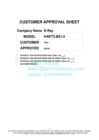
- 1. 1 ALL RIGHTS STRICTLY RESERVED. ANY PORTION OF THIS PAPER SHALL NOT BE REPRODUCED, COPIED, OR TRANSFORMED TO ANY OTHER FORMS WITHOUT PERMISSION FROM AU OPTRONICS CORP. CUSTOMER APPROVAL SHEET Company Name E-Ray MODEL H497TLB01.4 CUSTOMER APPROVED Title : Name : □ APPROVAL FOR SPECIFICATIONS ONLY (Spec. Ver. ) □ APPROVAL FOR SPECIFICATIONS AND ES SAMPLE (Spec. Ver. ) □ APPROVAL FOR SPECIFICATIONS AND CS SAMPLE (Spec. Ver. ) □ CUSTOMER REMARK : Panox Display sales@panoxdisplay.com skype: panoxwesley More LCD Displays On WWW.PANOXDISPLAY.COM
- 2. 2 ALL RIGHTS STRICTLY RESERVED. ANY PORTION OF THIS PAPER SHALL NOT BE REPRODUCED, COPIED, OR TRANSFORMED TO ANY OTHER FORMS WITHOUT PERMISSION FROM AU OPTRONICS CORP. Doc. version : 1.8 Total pages : 28 Date : 2015/07/21 Product Specification 5.0" Color AMOLED w/t On-Cell Touch Module MODEL NAME: H497TLB01.4 AUO Product P/N: 95.04H60.400 < >Preliminary Specification ◆ < >Final Specification Note: The content of this specification is subject to change. © AU Optronics All Rights Reserved, Do Not Copy. Panox Display sales@panoxdisplay.com skype: panoxwesley More LCD Displays On WWW.PANOXDISPLAY.COM
- 3. Version 1.8 Page: 3/31 3 ALL RIGHTS STRICTLY RESERVED. ANY PORTION OF THIS PAPER SHALL NOT BE REPRODUCED, COPIED, OR TRANSFORMED TO ANY OTHER FORMS WITHOUT PERMISSION FROM AU OPTRONICS CORP. Record of Revision Version Revise Date Page Content 0.0 Aug. 23, 2013 First Draft 0.1 Aug. 28, 2013 Add EE setting 0.2 Oct. 16, 2013 Spec. modified. 0.3 Nov. 6, 2013 15,16,18,21 Change Power on sequence and Power off sequence. 0.4 Nov. 28, 2013 18 ~ 21 Change Initial code. 0.5 Dec. 13, 2013 18 ~ 21 Add VESA standard / Change power consumption & initial code/ Module 0.6 Jan. 08, 2014 6 Revised pin 27 MIPI DSI data3+, pin 28 MIPI DSI data3- 0.7 Apr, 02, 2014 21 Add description on Display Timing 0.8 Nov. 06, 2014 4 Add VIDEO mode on Driver IC remark 0.8 Nov. 06, 2014 28 Add Precaution 0.9 Dec. 30, 2014 8 Update white pattern current & max current 4 Touch IC supports wakeup gesture (double click and swipe) 22 Revised optical Spec: color temperature 1.0 Jan. 09, 2015 27 Revised reliability test condition 1.1 Jan. 14, 2015 5~7 Add TP Spec 5 Add TP discription. 20 Modified initial code 1.2 Jan. 23, 2015 34~35 Glass thickness tolerance 1.3 Mar.09, 2015 Modified format, add uniformity Spec. 1.4 Mar.12, 2015 20 Add color temperature. 1.5 Mar.19, 2015 5 Modified connector model name 1.6 May. 08, 2015 27, 28 Add Main FPC silver ink, alignment mark, and EMI tape. 4 Add description of NC May. 19, 2015 20 Modifed viewing angle CR, cross talk description May. 28, 2015 6 Modified Pin assignment: OVDD Detect 1.7 May.29. 2015 15 Add more discription of power-on sequence 20~22 Add Touch Panel IIC address 6 Modified Pin assignment (Pin 32) 17 Modified initial code 1.8 Jul., 21, 2015 30~31 Drawing: modifed EMI tape Panox Display sales@panoxdisplay.com skype: panoxwesley More LCD Displays On WWW.PANOXDISPLAY.COM
- 4. Version 1.8 Page: 4/31 4 ALL RIGHTS STRICTLY RESERVED. ANY PORTION OF THIS PAPER SHALL NOT BE REPRODUCED, COPIED, OR TRANSFORMED TO ANY OTHER FORMS WITHOUT PERMISSION FROM AU OPTRONICS CORP. Contents A. General Specification ..................................................................................................................................5 1. AMOELD Panel Physical Specifications ...............................................................................................5 2. FPC Pin Assignment .............................................................................................................................5 3. Absolute Maximum Ratings...................................................................................................................6 B. DC Characteristics.......................................................................................................................................7 A. Operation Conditions.............................................................................................................................7 B. Display Current Consumption ...............................................................................................................7 C. Touch Panel Current Consumption .......................................................................................................8 C. AC Characteristics.......................................................................................................................................9 1. Display AC Characteristics....................................................................................................................9 2. Display RESET Timing Characteristics ...............................................................................................12 3. Touch Panel Timing Characteristics ....................................................................................................13 4. Operating Sequence ...........................................................................................................................15 D. Touch Specifications .................................................................................................................................19 E. Touch Panel IIC address............................................................................................................................20 F. Optical Specifications................................................................................................................................22 G. Reliability Test Items..................................................................................................................................27 H. Precaution...................................................................................................................................................28 I. Packing .......................................................................................................................................................29 J. Outline Demension ....................................................................................................................................30 Panox Display sales@panoxdisplay.com skype: panoxwesley More LCD Displays On WWW.PANOXDISPLAY.COM
- 5. Version 1.8 Page: 5/31 5 ALL RIGHTS STRICTLY RESERVED. ANY PORTION OF THIS PAPER SHALL NOT BE REPRODUCED, COPIED, OR TRANSFORMED TO ANY OTHER FORMS WITHOUT PERMISSION FROM AU OPTRONICS CORP. A. General Specification 1. AMOELD Panel Physical Specifications 2. FPC Pin Assignment Recommended connector: 39pins ZIF connector P/N: FF20-39A-R11A-B-3H # Pin_name I/O Description 1 GND Power Ground 2 NC No connection 3 TP_RESX I Touch panel reset 4 TP_SCL I/O Touch panel I2C clock 5 TP_SDA I/O Touch panel I2C data 6 TP_INT I/O Touch panel interrupt output 7 TP_VDDI Power Touch panel digital supply 8 TP_VCC Power Touch panel analog supply 9 NC No connection 10 VCI Power Driver IC analog supply 11 GND Power Ground 12 D3N I MIPI DSI data3- 13 D3P I MIPI DSI data3+ 14 GND Power Ground 15 D0N I/O MIPI DSI data0- 16 D0P I/O MIPI DSI data0+ 17 GND Power Ground 18 CKN I MIPI DSI clock- 19 CKP I MIPI DSI clock+ 20 GND Power Ground 21 D1N I MIPI DSI data0- 22 D1P I MIPI DSI data0+ 23 GND Power Ground 24 D2N I MIPI DSI data2- 25 D2P I MIPI DSI data2+ No. Item Spec. Remark 1 Screen Size (inch) 4.97” 2 Display Resolution (dot) 720xRGBx1280 3 Active Area (mm) 61.92 (H)×110.08(V) 4 Pixel Configuration Real R.G.B 5 Display Color 16.7M 6 Interface MIPI DSI VIDEO mode 7 Outline Dimension (mm) 65.92 (H) × 118.64(V) × 1.00(T) AMOLED w/ on-cell touch function 8 Touch IC S3402 Synaptics 9 Multi-Finger Touch 10 Panox Display sales@panoxdisplay.com skype: panoxwesley More LCD Displays On WWW.PANOXDISPLAY.COM
- 6. Version 1.8 Page: 6/31 6 ALL RIGHTS STRICTLY RESERVED. ANY PORTION OF THIS PAPER SHALL NOT BE REPRODUCED, COPIED, OR TRANSFORMED TO ANY OTHER FORMS WITHOUT PERMISSION FROM AU OPTRONICS CORP. 26 GND Power Ground 27 VDDI Power Driver IC digital supply 28 RESX I This signal will reset the device and must be applied to properly initialize the chip. Signal is active low. 29 TE O Sync signal from driver IC 30 OTP_PWR Power Driver IC R/W use only,system side must floating 31 NC No connection 32 NC No connection 33 NC No connection 34 VBAT Power panel power supply 35 VBAT Power panel power supply 36 VBAT Power panel power supply 37 VBAT Power panel power supply 38 VBAT Power panel power supply 39 GND Power Ground Note. I:Input pin; O: Output pin; P:Power pin; NC: No connection n; I/O: In-out pin 3. Absolute Maximum Ratings Item Symbol Min. Max. Unit Power IC Power supply VBAT - +4.5 V Digital Power supply VDDI -0.3 +2.0 V Analog Power supply VCI -0.3 +4.0 V Touch analog power supply TP_VCC -0.3 +4.0 V Touch digital power supply TP_VDDI -0.3 +2.0 V Note : If the module exceeds the absolute maximum ratings, it may be damaged permanently. Panox Display sales@panoxdisplay.com skype: panoxwesley More LCD Displays On WWW.PANOXDISPLAY.COM
- 7. Version 1.8 Page: 7/31 7 ALL RIGHTS STRICTLY RESERVED. ANY PORTION OF THIS PAPER SHALL NOT BE REPRODUCED, COPIED, OR TRANSFORMED TO ANY OTHER FORMS WITHOUT PERMISSION FROM AU OPTRONICS CORP. B. DC Characteristics A. Operation Conditions Item Symbol Min. Typ. Max. Unit Remark Panel Power supply VBAT 2.9 3.7 4.5 V Digital Power supply VDDI 1.65 1.8 1.95 V Analog Power supply VCI 2.7 3.1 3.6 V H Level VIH 0.8*VDDI - VDDI V Input Signal Voltage L Level VIL 0 - 0.2*VDDI V RESX H Level VOH 0.7*VDDI - VDDI V Output Signal Voltage L Level VOL 0 - 0.3*VDDI V TE Touch analog power supply TP_VCC 2.7 3.1 3.6 V Touch digital power supply TP_VDDI 1.65 1.8 1.95 V Note 1: The operation is guaranteed under the recommended operating conditions only. The operation is not guaranteed if a quick voltage change occurs during the operation. To prevent the noise, a bypass capacitor must be inserted into the line closed to the power pin. B. Display Current Consumption Note 1: VBAT input 2.9V, IBAT maximum current enhance to 460mA. Note 2: Based on white pattern. MIPI-DSI frame rate 60Hz video mode. Note 3: Display off. RESX = high Mode Symbol Condition Min. Typ. Max. Unit Remark IBAT - 300 360 mA Note1 IVCI - 60 80 mA Note2 Normal IVDDI - 1 10 mA Note2 IOVDD/OVS S - - <1 mA Note3 IVCI - - <1 mA Note3 Deep Standby (DSTB=1) IVDDI VBAT = 3.7V VCI = 3.1V VDDI = 1.8V - - <1 µA Note3 Panox Display sales@panoxdisplay.com skype: panoxwesley More LCD Displays On WWW.PANOXDISPLAY.COM
- 8. Version 1.8 Page: 8/31 8 ALL RIGHTS STRICTLY RESERVED. ANY PORTION OF THIS PAPER SHALL NOT BE REPRODUCED, COPIED, OR TRANSFORMED TO ANY OTHER FORMS WITHOUT PERMISSION FROM AU OPTRONICS CORP. C. Touch Panel Current Consumption Mode Symbol Condition min Typ. Max Unit ITP_VDDI - 13 14.3 mA Active (1 finger) ITP_VCC - 12.5 13.75 mA ITP_VDDI - 18.5 20.35 mA Active (10 finger) ITP_VCC - 12.5 13.75 mA ITP_VDDI - 0.4 0.44 mA Normal Operation ITP_VCC - 0.35 0.39 mA ITP_VDDI - 13.3 14.6 µA Sensor Sleep (Deep sleep) ITP_VCC TP_VDDI = 1.8V TP_VCC=3.1V Report Rate: 100Hz Doze Interval: 30 ms (26Rx x 15Tx) - 8 8.8 µA Panox Display sales@panoxdisplay.com skype: panoxwesley More LCD Displays On WWW.PANOXDISPLAY.COM
- 9. Version 1.8 Page: 9/31 9 ALL RIGHTS STRICTLY RESERVED. ANY PORTION OF THIS PAPER SHALL NOT BE REPRODUCED, COPIED, OR TRANSFORMED TO ANY OTHER FORMS WITHOUT PERMISSION FROM AU OPTRONICS CORP. C. AC Characteristics 1. Display AC Characteristics HS Data Transmission Burst HS clock transmission Turnaround Procedure Panox Display sales@panoxdisplay.com skype: panoxwesley More LCD Displays On WWW.PANOXDISPLAY.COM
- 10. Version 1.8 Page: 10/31 10 ALL RIGHTS STRICTLY RESERVED. ANY PORTION OF THIS PAPER SHALL NOT BE REPRODUCED, COPIED, OR TRANSFORMED TO ANY OTHER FORMS WITHOUT PERMISSION FROM AU OPTRONICS CORP. Timing Parameters Symbol Description Min Typ Max Unit TCLK-POST Time that the transmitter continues to send HS clock after the last associated Data Lane has transitioned to LP Mode. Interval is defined as the period from the end of THS-TRAIL to the beginning of TCLK- TRAIL . 60ns + 52*UI ns TCLK-TRAIL Time that the transmitter drives the HS-0 state after the last payload clock bit of a HS transmission burst. 60 ns THS-EXIT Time that the transmitter drives LP- 11 following a HS burst. 300 ns TCLK-TERM- EN Time for the Clock Lane receiver to enable the HS line termination, starting from the time point when Dn crosses VIL,MAX . Time for Dn to reach VTERM-EN 38 ns TCLK- PREPARE Time that the transmitter drives the Clock Lane LP-00 Line state immediately before the HS-0 Line state starting the HS transmission. 38 95 ns TCLK-PRE Time that the HS clock shall be driven by the transmitter prior to any associated Data Lane beginning the transition from LP to HS mode. 8 UI TCLK- PREPARE + TCLK- ZERO TCLK-PREPARE + time that the transmitter drives the HS-0 state prior to starting the Clock. 300 ns TD-TERM-EN Time for the Data Lane receiver to enable the HS line termination, starting from the time point when Dn crosses VIL,MAX . Time for Dn to reach VTERM-EN 35 ns +4*UI THS- PREPARE Time that the transmitter drives the Data Lane LP-00 Line state immediately before the HS-0 Line state starting the HS transmission 40ns + 4*UI 85 ns + 6*UI ns Panox Display sales@panoxdisplay.com skype: panoxwesley More LCD Displays On WWW.PANOXDISPLAY.COM
- 11. Version 1.8 Page: 11/31 11 ALL RIGHTS STRICTLY RESERVED. ANY PORTION OF THIS PAPER SHALL NOT BE REPRODUCED, COPIED, OR TRANSFORMED TO ANY OTHER FORMS WITHOUT PERMISSION FROM AU OPTRONICS CORP. THS- PREPARE + THS-ZERO THS-PREPARE + time that the transmitter drives the HS-0 state prior to transmitting the Sync sequence. 145ns + 10*UI ns THS-TRAIL Time that the transmitter drives the flipped differential state after last payload data bit of a HS transmission burst 60ns + 4*UI ns TLPX(M) Transmitted length of any Low-Power state period of MCU to display module 50 150 ns TTA-SURE(M) Time that the display module waits after the LP-10 state before transmitting the Bridge state (LP-00) during a Link Turnaround. TLPX(M) 2*TLPX( M) ns TLPX(D) Transmitted length of any Low-Power state period of display module to MCU 50 150 ns TTA-GET(D) Time that the display module drives the Bridge state (LP-00) after accepting control during a Link Turnaround. 5*TLPX(D) ns TTA-GO(D) Time that the display module drives the Bridge state (LP-00) before releasing control during a Link Turnaround. 4*TLPX(D) ns TTA-SURE(D) Time that the MPU waits after the LP-10 state before transmitting the Bridge state (LP-00) during a Link Turnaround. TLPX(D) 2*TLPX( D) ns Panox Display sales@panoxdisplay.com skype: panoxwesley More LCD Displays On WWW.PANOXDISPLAY.COM
- 12. Version 1.8 Page: 12/31 12 ALL RIGHTS STRICTLY RESERVED. ANY PORTION OF THIS PAPER SHALL NOT BE REPRODUCED, COPIED, OR TRANSFORMED TO ANY OTHER FORMS WITHOUT PERMISSION FROM AU OPTRONICS CORP. 2. Display RESET Timing Characteristics Reset input timing Internal Status !RES tRESW tREST Resetting Initial Condition (Default for H/W reset) Shorter than 15µs Normal Operation RESX Timing Parameters Symbol Parameter Related Pins MIN TYP MAX Note Unit tRESW *1) Reset low pulse width RESX 15 - - - µs - - - 5 When reset applied during Sleep in mode ms tREST *2) Reset complete time - - 120 When reset applied during Sleep out mode ms Note 1. Spike due to an electrostatic discharge on RESX line does not cause irregular system reset according to the table below. RESX Pulse Action Shorter than 5µs Invalid Reset Longer than 15µs Valid Reset Between 5µs and 15µs Reset Initialization Precedure Note 2. During the resetting period, the display will be blanked (The display is entering blanking sequence, which maximum time is 120 ms, when Reset Starts in Sleep Out –mode. The display remains the blank state in Sleep In –mode) and then return to Default condition for H/W reset. Note 3. During Reset Complete Time, data in OTP will be latched to internal register during this period. This loading is done every time when there is H/W reset complete time (tREST) within 5ms after a rising edge of RESX. Note 4. Spike Rejection also applies during a valid reset pulse as shown below: Note 5. It is necessary to wait 5msec after releasing RESX before sending commands. Also Sleep Out command cannot be sent for 120msec. More LCD Displays On WWW.PANOXDISPLAY.COM
- 13. Version 1.8 Page: 13/31 13 ALL RIGHTS STRICTLY RESERVED. ANY PORTION OF THIS PAPER SHALL NOT BE REPRODUCED, COPIED, OR TRANSFORMED TO ANY OTHER FORMS WITHOUT PERMISSION FROM AU OPTRONICS CORP. 3. Touch Panel Timing Characteristics I2C timing Timing Parameters Standard- Mode Host Fast-Mode Host Symbol Parameter Min. Max. Min. Max. Unit fSCL SCL clock frequency - 100 - 400 kHz Tcstr Stretch time - 25 - 25 µs Thd;sta Hold time (repeated) START condition. After this period, the first clock pulse is generated. 4.0 - 0.6 - µs Tlow LOW period of the SCL clock 4.7 - 1.3 - µs Thigh HIGH period of the SCL clock 4.0 - 0.6 - µs Tsu;sta Set-up time for a repeated START condition 4.7 - 0.6 - µs Thd;dat Data hold time 0 3.45 0 0.9 µs Thd;dato Data out hold time - 0 - 0 µs Tsu;dat Data set-up time 250 - 100 - ns Tr Rise time of both SDA and SCL signals - 1000 20 + 0.1 Cb 300 ns Tf Fall time of both SDA and SCL signals - 3000 20 + 0.1 Cb 300 ns Tsu;sto Set-up time for STOP condition 4.0 - 0.6 - µs Tbuf Bus free time between a STOP and START condition 4.7 - 1.3 - µs Cb Capacitive load for each bus line - 400 - 400 pF VnL Noise margin at the LOW level for each connected device (including hysteresis) 0.1 TP_VDDI 0.1 TP_VDDI V VnH Noise margin at the HIGH level for each connected device (including hysteresis) 0.2 TP_VDDI - 0.2 TP_VDDI - V TP_SDA TP_SCL More LCD Displays On WWW.PANOXDISPLAY.COM
- 14. Version 1.8 Page: 14/31 14 ALL RIGHTS STRICTLY RESERVED. ANY PORTION OF THIS PAPER SHALL NOT BE REPRODUCED, COPIED, OR TRANSFORMED TO ANY OTHER FORMS WITHOUT PERMISSION FROM AU OPTRONICS CORP. Touch Panel RESET Timing Characteristics Reset input timing Timing Parameters Symbol Min. Max. Unit Treset (TP_RESX) 100 - ns Tbl_start - 2 ms Tbl_active - 11 ms Treboot - 16 ms TP_RESX TP_INT More LCD Displays On WWW.PANOXDISPLAY.COM
- 15. Version 1.8 Page: 15/31 15 ALL RIGHTS STRICTLY RESERVED. ANY PORTION OF THIS PAPER SHALL NOT BE REPRODUCED, COPIED, OR TRANSFORMED TO ANY OTHER FORMS WITHOUT PERMISSION FROM AU OPTRONICS CORP. 4. Operating Sequence State Diagram Display Power on / off Sequence IC setting Reset VBAT VDDI VCI Initial setting sleep out display on >5ms >5ms >30ms >5ms Power On Sequence: >0ms >130ms More LCD Displays On WWW.PANOXDISPLAY.COM
- 16. Version 1.8 Page: 16/31 16 ALL RIGHTS STRICTLY RESERVED. ANY PORTION OF THIS PAPER SHALL NOT BE REPRODUCED, COPIED, OR TRANSFORMED TO ANY OTHER FORMS WITHOUT PERMISSION FROM AU OPTRONICS CORP. Touch Panel Power on Sequence Symbol Min. Max. Unit Tpowerupt - 60 ms Tbl_start (bootloader start) - 46 ms Tbl_active (bootloader active) - 11 ms TP_SDA TP_SCL TP_INT More LCD Displays On WWW.PANOXDISPLAY.COM
- 17. Version 1.8 Page: 17/31 17 ALL RIGHTS STRICTLY RESERVED. ANY PORTION OF THIS PAPER SHALL NOT BE REPRODUCED, COPIED, OR TRANSFORMED TO ANY OTHER FORMS WITHOUT PERMISSION FROM AU OPTRONICS CORP. Display Initial Setting Item Parameter qt'y address P0 P1 P2 P3 P4 P5 P6 P7 P8 P9 P10 1 5 F0 55 AA 52 08 00 2 3 B0 00 10 10 3 1 BA 60 4 7 BB 00 00 00 00 00 00 00 5 8 C0 C0 04 00 20 02 E4 E1 C0 6 8 C1 C0 04 00 20 04 E4 E1 C0 7 5 F0 55 AA 52 08 02 8 5 EA 7F 20 00 00 00 9 1 CA 04 10 1 E1 00 11 1 E2 0A 12 1 E3 40 13 4 E7 00 00 00 00 14 8 ED 48 00 E0 13 08 00 91 08 15 6 FD 00 08 1C 00 00 01 16 11 C3 11 24 04 0A 02 04 00 1C 10 F0 00 17 5 F0 55 AA 52 08 03 18 1 E0 00 19 6 F1 00 00 00 00 00 15 20 1 F6 08 21 5 F0 55 AA 52 08 05 22 5 C3 00 10 50 50 50 23 2 C4 00 14 24 1 C9 04 25 5 F0 55 AA 52 08 01 26 3 B0 06 06 06 27 3 B1 14 14 14 28 3 B2 00 00 00 29 3 B4 66 66 66 30 3 B5 44 44 44 31 3 B6 54 54 54 32 3 B7 24 24 24 33 3 B9 04 04 04 34 3 BA 14 14 14 35 3 BE 22 38 78 36 1 35 00 More LCD Displays On WWW.PANOXDISPLAY.COM
- 18. Version 1.8 Page: 18/31 18 ALL RIGHTS STRICTLY RESERVED. ANY PORTION OF THIS PAPER SHALL NOT BE REPRODUCED, COPIED, OR TRANSFORMED TO ANY OTHER FORMS WITHOUT PERMISSION FROM AU OPTRONICS CORP. Display Timing More LCD Displays On WWW.PANOXDISPLAY.COM
- 19. Version 1.8 Page: 19/31 19 ALL RIGHTS STRICTLY RESERVED. ANY PORTION OF THIS PAPER SHALL NOT BE REPRODUCED, COPIED, OR TRANSFORMED TO ANY OTHER FORMS WITHOUT PERMISSION FROM AU OPTRONICS CORP. D. Touch Specifications No. Item Spec. Remark 1 Touch IC S3402 Synaptics 2 Multi-Finger 10 3 Report Rate 100Hz ≧ Accuracy. 2.0mm ≦ 4 Performance Linearity 2.0mm ≦ Note 1 Double tape 0.6se >∆t >(1/ report rate) ∆t=Ttape1-Ttape2 5 Wakeup Gesture Swipe ∆S > 20mm & 50mm/sec>V>20mm/sec ∆S :swipe distance V :swipe velocity Note 1: Draw straight lines on the X axis, Y axis and diagonal axis with 6mm diameter copper slug at 50mm/sec drawing speed. And, drawing area is defined as below figure shown, which according to AA area and slig size. Accuracy= Max{|(y-m0x-b)/(m0^2+1)^0.5|} Linearity= Max{|(y-m0’x-b’)/(m0’^2+1)^0.5|} where (x,y)s are the TP IC reported coordinates, Y=m0X+b Real Line Equation Y’ =m0’ X’ +b’ Fitting Line Equation 1 2 3 4 5 6 7 8 9 1 0 1 1 1 2 Real Line Fitting line Reported points to fit a line. (3,3) (107.58, 59.42) Unit: mm More LCD Displays On WWW.PANOXDISPLAY.COM
- 20. Version 1.8 Page: 20/31 20 ALL RIGHTS STRICTLY RESERVED. ANY PORTION OF THIS PAPER SHALL NOT BE REPRODUCED, COPIED, OR TRANSFORMED TO ANY OTHER FORMS WITHOUT PERMISSION FROM AU OPTRONICS CORP. E. Touch Panel IIC address Reading Manufacturer ID: IIC address (7 bits) = 0x20 Although a host would not normally need to read the Manufacturer ID register provided by the RMI4 interface, reading this register is a good first step in verifying that the host and Touch Controller are communicating. The Manufacturer ID register belongs to the group of Function $01 query registers. The addresses of these registers vary between different Synaptics RMI4-over-I2C Touch Controllers. The Manufacturer ID register always returns data $01. Figure A gives an example of the resulting bus transaction, in the format typically used to describe I2C transactions. The symbol meanings are listed in Table A. The shaded areas indicate bus activity by the Touch Controller. In this example, assume the slave address of the device is $20, with the Manufacturer ID register at $E1. Tabel A. Symbol Meaning S I2C bus Start condition. This is a falling edge on SDA while SCL is high. Sr Repeated Start condition. Same as S. Note that hosts that cannot generate Repeated Starts may use a Stop condition (P) followed by a another Start (S) instead. P I2C Stop condition. This is a rising edge on SDA while SCL is high. A I2C acknowledge (ACK). The data receiver pulls SDA low during a high pulse on SCL driven by the transmitter. N I2C not acknowledge (NACK). The data receiver lets SDA remain high during a high pulse on SCL driven by the transmitter. Wr ‘Write’ bit. This has a value of 0. Rd ‘Read’ bit. This has a value of 1. Using register: A. Page Select Addr Name Bit7 Bit6 Bit5 Bit4 Bit3 Bit2 Bit1 Bit0 Access 0x00FF Page Select Page W Description Set Page 0=0x00 S Slave Address $20 Wr 0 A Register Address $E1 A Sr Slave Address $20 Rd 1 A Data $01 N P Figure A. Read Manufacturer ID command 7 bits 7 bits 8 bits 1 bit 1 bit 8 bits More LCD Displays On WWW.PANOXDISPLAY.COM
- 21. Version 1.8 Page: 21/31 21 ALL RIGHTS STRICTLY RESERVED. ANY PORTION OF THIS PAPER SHALL NOT BE REPRODUCED, COPIED, OR TRANSFORMED TO ANY OTHER FORMS WITHOUT PERMISSION FROM AU OPTRONICS CORP. B. Communicating: Address=0x0006 is used to read coordinate. It must continue to read 10 fingers data every time Page 0x00 Registers Addr Name Bit7 Bit6 Bit5 Bit4 Bit3 Bit2 Bit1 Bit0 Access F12_2D_DATA01(00)/00 Object Type and Status 0 Object Type and Status R W F12_2D_DATA01(00)/01 Object Data 0 X LSB R W F12_2D_DATA01(00)/02 Object Data 0 X MSB R W F12_2D_DATA01(00)/03 Object Data 0 Y LSB R W F12_2D_DATA01(00)/04 Object Data 0 Y MSB R W F12_2D_DATA01(00)/05 Object Data 0 Z R W F12_2D_DATA01(00)/06 Object Data 0 Wx R W 0x0006 F12_2D_DATA01(00)/07 Object Data 0 Wy R W Description Object Type and Status (F12_2D_Data1(N)/0) ○ 0x00 = No object ○ 0x01 = Finger ○ 0x02 = Stylus ○ 0x03 = Palm ○ 0x04 = Unclassified ○ 0x05 = Reserved ○ 0x06 = Gloved Finger X and Y position data (MSB) These registers report the most-significant bits of the absolute X and Y position data. X and Y position data (LSB) This register contains the least-significant bits for both the X and Y absolute position information. Z This field reports the amount of finger contact or finger signal strength, which often serves as a rough estimate of finger pressure. When Z = 0, the More LCD Displays On WWW.PANOXDISPLAY.COM
- 22. Version 1.8 Page: 22/31 22 ALL RIGHTS STRICTLY RESERVED. ANY PORTION OF THIS PAPER SHALL NOT BE REPRODUCED, COPIED, OR TRANSFORMED TO ANY OTHER FORMS WITHOUT PERMISSION FROM AU OPTRONICS CORP. position cannot be measured and the X and Y Position registers are left unchanged. By default Z is taken as 0 whenever the device’s built-in algorithms determine that no finger is present. Wx, Wy These fields report the estimated finger width as an unsigned integer, where 0 represents an extremely narrow finger and 15 represents an extremely wide contact such as a palm laid flat on the sensor. The ratio of Wx and Wy provides an estimate of the finger contact aspect ratio. F. Optical Specifications More LCD Displays On WWW.PANOXDISPLAY.COM
- 23. Version 1.8 Page: 23/31 23 ALL RIGHTS STRICTLY RESERVED. ANY PORTION OF THIS PAPER SHALL NOT BE REPRODUCED, COPIED, OR TRANSFORMED TO ANY OTHER FORMS WITHOUT PERMISSION FROM AU OPTRONICS CORP. Item Min. Typ. Max. Unit Remark Brightness 250 275 300 nits Note 3 Contrast Ratio @25deg 10000 -- -- Note 5 Color Temperature 7000 7500 8000 K Note 3 Top 80° -- -- deg Bottom 80° -- -- deg Left 80° -- -- deg Viewing Angle CR1600 Right 80° -- -- deg Note 7 Brightness Uniformity 275nits 70% -- -- Note 6 Optical Switching Time +25° B/W(Tr+Tf)/2 -- -- 1 ms Note 4 CIE1931 x 0.28 0.30 0.32 W CIE1931 y 0.29 0.31 0.33 CIE1931 x 0.645 0.675 0.705 R CIE1931 y 0.295 0.325 0.355 CIE1931 x 0.186 0.236 0.286 G CIE1931 y 0.661 0.711 0.761 CIE1931 x 0.090 0.130 0.170 Color B CIE1931 y 0.025 0.065 0.105 NTSC CIE x , y 80 100 -- % Delt x 0.015 Color Uniformity @ White Pattern Delt y 0.015 Note 6 Life time LT95 25C° 100 -- -- hrs Note 9 Flicker -- -- -30 db Note 8 Crosstalk Max (V, H) -- -- 5.0 % Note 10 Gamma γ 2.0 2.2 2.4 Note 11 Note 1: Ambient temperature =25 ±2 , mea ℃ ℃ sured by CA-310. Note 2: To be measured in the dark room. Note 3: The brightness measurement shall be done at the center of the display with a full white image. Note 4: Optical Switching Time: The optical switching time measurements should be performed at driven BLACK and driven WHITE at typ. brightness setting by the driving techniques specified. The luminance should be measured with the emitting display and the detector at More LCD Displays On WWW.PANOXDISPLAY.COM
- 24. Version 1.8 Page: 24/31 24 ALL RIGHTS STRICTLY RESERVED. ANY PORTION OF THIS PAPER SHALL NOT BE REPRODUCED, COPIED, OR TRANSFORMED TO ANY OTHER FORMS WITHOUT PERMISSION FROM AU OPTRONICS CORP. θ=0° and ψ=90° . The rise time tr is the time between a 10% optically response of the display and a 90% optically response of the display. The fall time tf is the time between a 10% optically response of the display and a 90% optically response to the display. The response time is defined as the average of the rise time and the fall time. Note 5: Definition of contrast ratio: Contrast ratio is calculated with the following formula: Contrast ratio (CR)= Note 6: Uniformity. Refer to figure as below Delt x = (Maximum value of CIEx from S0 to S8) – (Minimum value of CIEx from S0 to S8) Delt y = (Maximum value of CIEy from S0 to S8) – (Minimum value of CIEy from S0 to S8) Photo detector output when OLED is at “White” Photo detector output when OLED is at “Black More LCD Displays On WWW.PANOXDISPLAY.COM
- 25. Version 1.8 Page: 25/31 25 ALL RIGHTS STRICTLY RESERVED. ANY PORTION OF THIS PAPER SHALL NOT BE REPRODUCED, COPIED, OR TRANSFORMED TO ANY OTHER FORMS WITHOUT PERMISSION FROM AU OPTRONICS CORP. Note 7: Definition of viewing angle : The optical performance is specified as the driver IC located at =270° Note 8: Flicker The flicker level is defined using Fast Fourier Transformation (FTT) as follows: where fFFTC(n) is the nth FFT coefficient, and fFFTC(0) is the 0th FFT coefficient which is DC component. FS(Hz) is the flicker sensitivity as a function of frequency. The flicker level shall be measured with the test pattern in below. The gray leves of test pattern is 128. Note 9: Time to 95% Luminance Test @ full white pattern, the brightness decay from 100% to 95%. More LCD Displays On WWW.PANOXDISPLAY.COM
- 26. Version 1.8 Page: 26/31 26 ALL RIGHTS STRICTLY RESERVED. ANY PORTION OF THIS PAPER SHALL NOT BE REPRODUCED, COPIED, OR TRANSFORMED TO ANY OTHER FORMS WITHOUT PERMISSION FROM AU OPTRONICS CORP. Note 10: Cross-talk Note 11: Gamma spec. is based on Gray level 255, 250, 244, 240, 232, 224, 206, 192, 160, 128, 95, 63, 47 31. Gray128 Gray128 Gray128 Gray 255 Gray 0 More LCD Displays On WWW.PANOXDISPLAY.COM
- 27. Version 1.8 Page: 27/31 27 ALL RIGHTS STRICTLY RESERVED. ANY PORTION OF THIS PAPER SHALL NOT BE REPRODUCED, COPIED, OR TRANSFORMED TO ANY OTHER FORMS WITHOUT PERMISSION FROM AU OPTRONICS CORP. G. Reliability Test Items Category No. Test items Conditions Remark 1 High Temp. Operation Ta= 70℃ 168hrs 2 High Temp. Storage Ta= 70℃ 168hrs 3 Low Temp. Operation Ta= -40℃ 168hrs 4 Low Temp. Storage Ta= -40℃ 168hrs 5 High Temp./Humi. Operation Ta= 40 . 95% RH ℃ 168hrs 6 Thermal Shock -40 ~70 , Dwell for 30 min. 30 ℃ ℃ cycles. Non-operation Judge criteria: No function defect Reliability (Environment) 7 Low Pressure Storage Condition: 40,000 ft, room temperature, 48hrs. Criterion: Normal performance after recovery time. Non- operation 8 Shock Test Half Sine, 400G, duration time 2 ms, One shock for each surfaces,total 6 shocks Non- operation 9 Random Vibration Test 0.025G2/Hz, 10~500Hz Nominal 3.5Grms in each axis, 30 minutes each axis Non- operation 10 Sinusoidal Vibration Test 0.5 octave / minutes sweep rate One sweep, 10 to 500Hz, all 3 axes (X, Y, Z) Fixture used: Fasten the specimen to the vibration table Power is OFF Non- operation 11 FPC Bending Connector side: Bending FPC with 180°both clockwise and counterclockwise OLED side: Bending FPC with 180°both clockwise and counterclockwise minimum 30 cycles for every side. Non- operation Reliability (Mechanical) 12 FPC connection insert/ Remove Insert/Remove Panel’s FPC for 15 cycles. IEC 61000-4-2 Air Discharge ±8KV ESD 13 Contact Discharge ±4KV There is no degradation of OLED performance after this test. Panel level. Grounding 15 Metal frame grounding The resistance between FPC ground pin and metal frame should be less than 1 Ohm before/after all reliability test More LCD Displays On WWW.PANOXDISPLAY.COM
- 28. Version 1.8 Page: 28/31 28 ALL RIGHTS STRICTLY RESERVED. ANY PORTION OF THIS PAPER SHALL NOT BE REPRODUCED, COPIED, OR TRANSFORMED TO ANY OTHER FORMS WITHOUT PERMISSION FROM AU OPTRONICS CORP. H. Precaution Please pay attention to the following items when you use the OLED Modules(Panel): 1. Do not twist or bend the module(panel) and prevent the unsuitable external force for display during assembly. 2. Adopt measures for good heat radiation. Be sure to use the module(panel) with in the specified temperature. 3. Avoid dust or oil mist during assembly. 4. Follow the correct power sequence while operating. Do not apply the invalid signal, otherwise, it will cause improper shut down and damage the module(panel). 5. Less EMI: it will be more safety and less noise. 6. Please operate module(panel) in suitable temperature. The response time brightness will drift by different temperature. 7. Avoid to display the fixed pattern (exclude the white pattern) in a long period, otherwise, it will cause image sticking. 8. Please be sure to turn-off the power when connecting or disconnecting the circuit. 9. Polarizer scratches easily, please handle it carefully. 10. Display surface never likes dirt or stains. 11. A dew drop may lead to destruction. Please wipe off any moisture before using module(panel). 12. Sudden temperature changes cause condensation, and it will cause polarizer damaged. 13. High temperature and humidity may degrade performance. Please do not expose the module(panel) to the direct sunlight and so on. 14. Acetic acid or chlorine compounds are not friends with AMOLED display module(panel). 15. Static electricity will damage the module(panel), please do not touch the module(panel) without any grounded device. 16. Please avoid any static electricity damage (ESD) during producing and operating. 17. Do not disassemble and reassemble the module(panel) by self. 18. Be careful do not touch the rear side directly. 19. No strong vibration or shock. It will cause module(panel) broken. 20. Storage the modules(panel) in suitable environment with regular packing. 21. Be careful of injury from a broken display module(panel). 22. Please avoid the pressure adding to the surface (front or rear side) of modules(panel), because it will cause the display non-uniformity or other function issue. 23. Touch code is decided by (1) cover lens type, (2) lens lamination parameters, and (3) customers’ hardware/software setting. Please be noted if above factors was changed, AUO need new samples to re-adjusted touch code. More LCD Displays On WWW.PANOXDISPLAY.COM
- 29. Version 1.8 Page: 29/31 29 ALL RIGHTS STRICTLY RESERVED. ANY PORTION OF THIS PAPER SHALL NOT BE REPRODUCED, COPIED, OR TRANSFORMED TO ANY OTHER FORMS WITHOUT PERMISSION FROM AU OPTRONICS CORP. I. Packing 紙箱尺寸:546mm x 406mm x 278mm 棧板尺寸:1150mmx840mmx132mm 1set for 20 tray (8pcs) +1 tray(空) =160pcs module 5 layer x4 boxes =20 boxes More LCD Displays On WWW.PANOXDISPLAY.COM
- 30. Version 1.8 Page: 30/31 30 ALL RIGHTS STRICTLY RESERVED. ANY PORTION OF THIS PAPER SHALL NOT BE REPRODUCED, COPIED, OR TRANSFORMED TO ANY OTHER FORMS WITHOUT PERMISSION FROM AU OPTRONICS CORP. J. Outline Demension More LCD Displays On WWW.PANOXDISPLAY.COM
- 31. Version 1.8 Page: 31/31 31 ALL RIGHTS STRICTLY RESERVED. ANY PORTION OF THIS PAPER SHALL NOT BE REPRODUCED, COPIED, OR TRANSFORMED TO ANY OTHER FORMS WITHOUT PERMISSION FROM AU OPTRONICS CORP. More LCD Displays On WWW.PANOXDISPLAY.COM