1.63 inch OLED 320X320 MIPI Square OLED
•
0 likes•18 views

Display Type AMOLED Display Brand AUO Interface MIPI Screen Size 1.63 Orientation Landscape Display Color Full Color Manufacturer AUO Resolution 320(RGB)×320 Driver IC COG Built-in RM69032 Consumption 138.4mW (Max.) Active Area (mm) 29.28(H)×29.28(V) mm Luminance 300 cd/m² (Typ.) Viewing Angle 80/80/80/80 (Min.)(CR≥1600) Color Depth 16.7M 103% Product Page https://www.panoxdisplay.com/amoled/1-63-amoled-full-color-320x320.html

Recommended
Recommended
More Related Content
Similar to 1.63 inch OLED 320X320 MIPI Square OLED
Similar to 1.63 inch OLED 320X320 MIPI Square OLED (20)
More from Panox Display
More from Panox Display (11)
Recently uploaded
Recently uploaded (20)
1.63 inch OLED 320X320 MIPI Square OLED
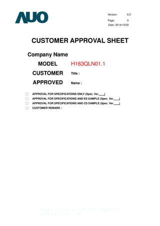
- 1. Version: 6.0 Page: 0 Date: 2014/10/02 CUSTOMER APPROVAL SHEET Company Name MODEL H163QLN01.1 CUSTOMER APPROVED Title : Name : □ APPROVAL FOR SPECIFICATIONS ONLY (Spec. Ver. ) □ APPROVAL FOR SPECIFICATIONS AND ES SAMPLE (Spec. Ver. ) □ APPROVAL FOR SPECIFICATIONS AND CS SAMPLE (Spec. Ver. ) □ CUSTOMER REMARK : Panox Dsipaly OLED/LCD Supplier panoxdisplay.com
- 2. ALL RIGHTS STRICTLY RESERVED. ANY PORTION OF THIS PAPER SHALL NOT BE REPRODUCED, COPIED, OR TRANSFORMED TO ANY OTHER FORMS WITHOUT PERMISSION FROM AU OPTRONICS CORP. Doc. version : 6.0 Total pages : Date : 2014/10/2 Product Specification 1.63" COLOR AMOLED MODULE MODEL NAME: H163QLN01 AUO Product P/N: 95.01H72.101 < >Preliminary Specification ◆ < >Final Specification Note: The content of this specification is subject to change. © 2014 AU Optronics All Rights Reserved, Do Not Copy. Panox Dsipaly OLED/LCD Supplier panoxdisplay.com
- 3. Version 6.0 Page: 2/25 2 ALL RIGHTS STRICTLY RESERVED. ANY PORTION OF THIS PAPER SHALL NOT BE REPRODUCED, COPIED, OR TRANSFORMED TO ANY OTHER FORMS WITHOUT PERMISSION FROM AU OPTRONICS CORP. Record of Revision Version Revise Date Page Content 0.0 Mar. 5, 2014 First Draft 1.0 Mar.18,2014 17 21 22 23 Revise H. Specifications_Optical characteristics Add I. Reliability test items_Vibration test Add J.packing Revise K.2D/3D drawing; 2.0 Apr.16,2014 7 11 14, 15 16 24 Add Idle power consumption & revise panel power Revise TE description Revise Initial Code for display optimization B500=0x05 -> 0x03; B501=0x05 -> 0x03; B502=0x05 -> 0x03 BA00=0x13 -> 0x03; BA01=0x13 -> 0x03; BA02=0x13 -> 0x03 BE00=0x22 -> 0x32 Revise CF description Revise K. 2D drawing 3.0 July.3,2014 24 Revise K. 2D drawing 4.0 July.17,2014 24 Revie 2D drawing for foam tape modified. 5.0 Aug.7,2014 25 Add Precaution 6.0 Oct. 6,2014 13 14 15 24 Revise Initial Code for display optimization BD00~BD04 =0x03 20 14 4B 00 BE00~BE04 =0x03 20 14 4B 01 BF00~BF04 =0x03 20 14 4B 00 EB00=0x02 E900~E902 = 0x00 36 38 B600=0x53 -> 0x55; B601=0x53 -> 0x55; B602=0x53 -> 0x55 B700=0x33 -> 0x36; B701=0x33 -> 0x36; B702=0x33 -> 0x36 CF03=0xEF -> 0XE8 Revie 2D drawing for foam tape modified. Panox Dsipaly OLED/LCD Supplier panoxdisplay.com
- 4. Version 6.0 Page: 3/25 3 ALL RIGHTS STRICTLY RESERVED. ANY PORTION OF THIS PAPER SHALL NOT BE REPRODUCED, COPIED, OR TRANSFORMED TO ANY OTHER FORMS WITHOUT PERMISSION FROM AU OPTRONICS CORP. Contents A. General Specification ..................................................................................................................................4 1. Physical Specifications..........................................................................................................................4 2. Module Block Diagram ..........................................................................................................................4 3. Panel Scan direction .............................................................................................................................4 B. Electrical Specifications..............................................................................................................................5 1. Main FPC Pin assignment — AMOLED Panel Input/Output Signal Interface.......................................5 2. Absolute maximum ratings....................................................................................................................6 C. Electrical Characteristics ............................................................................................................................7 1. DC Operating Conditions ......................................................................................................................7 2. Display Current Consumption ...............................................................................................................7 D. AC Characteristics.......................................................................................................................................8 1. MIPI Interface Characteristics ...............................................................................................................8 2. Display RESET Timing Characteristics ...............................................................................................10 3. TE Timing Characteristics ...................................................................................................................11 E. Recommended Operating Sequence .......................................................................................................12 1. Display Power on / off Sequence ........................................................................................................12 2. Display Initial code ..............................................................................................................................13 F. Brightness Control.....................................................................................................................................16 G. Application Circuit .....................................................................................................................................17 H. Specifications.............................................................................................................................................18 I. Reliability Test Items..................................................................................................................................22 J. Packing .......................................................................................................................................................23 K. Outline Demension (Tentative) .................................................................................................................24 Panox Dsipaly OLED/LCD Supplier panoxdisplay.com
- 5. Version 6.0 Page: 4/25 4 ALL RIGHTS STRICTLY RESERVED. ANY PORTION OF THIS PAPER SHALL NOT BE REPRODUCED, COPIED, OR TRANSFORMED TO ANY OTHER FORMS WITHOUT PERMISSION FROM AU OPTRONICS CORP. A. General Specification 1. Physical Specifications Item Description Remark 1 Screen Size (inch) 1.63” 2 Display Mode AMOLED 3 Display Resolution (dot) 320xRGBx320 4 Active Area (mm*mm) 29.28 (H)×29.28(V) 5 Pixel Configuration Hyper R.G.B 6 Display Color (M) 16.7 7 Brightness (nits) 300 8 Interface MIPI DSI 9 Outline Dimension (mm*mm*mm) 32.08 (H) × 36.48(V) × 0.7(T) cell+foam 2. Module Block Diagram 3. Panel Scan direction Driver IC Side (0,0) AMOLED Panel 320xRGBx320 GOA Driver IC GOA Panox Dsipaly OLED/LCD Supplier panoxdisplay.com
- 6. Version 6.0 Page: 5/25 5 ALL RIGHTS STRICTLY RESERVED. ANY PORTION OF THIS PAPER SHALL NOT BE REPRODUCED, COPIED, OR TRANSFORMED TO ANY OTHER FORMS WITHOUT PERMISSION FROM AU OPTRONICS CORP. B. Electrical Specifications 1. Main FPC Pin assignment — AMOLED Panel Input/Output Signal Interface Recommended connector: AXE520127 (Panasonic) FPC Pin_name I/O Description 1 ELVSS P AMOLED power Negative 2 ELVSS P AMOLED power Negative 3 ELVSS P AMOLED power Negative 4 VDD P Power supply for analog 5 IOVDD P Power supply for Interface system excep MIPI interface 6 GND P GND 7 TE O Vsync(vertical sync)signal output from panel to avoid tearing effect 8 MTP I MTP(need to indicate to connect GND or NC) 9 RESX I Device reset signal (0 : Enable ; 1: Disable ) 10 SWIRE O SWIRE signal for PWR IC control 11 ELVDD P AMOLED power positive 12 ELVDD P AMOLED power positive 13 ELVDD P AMOLED power positive 14 GND P GND 15 DSI_D0N I/O MIPI data negative signal 16 DSI_D0P I/O MIPI data positive signal 17 GND P GND 18 DSI_CLKN I MIPI strobe negative signal 19 DSI_CLKP I MIPI strobe postive signal 20 GND P GND Note: I = input ; O = output ; P = Power ; I/O = input / Output Panox Dsipaly OLED/LCD Supplier panoxdisplay.com
- 7. Version 6.0 Page: 6/25 6 ALL RIGHTS STRICTLY RESERVED. ANY PORTION OF THIS PAPER SHALL NOT BE REPRODUCED, COPIED, OR TRANSFORMED TO ANY OTHER FORMS WITHOUT PERMISSION FROM AU OPTRONICS CORP. 2. Absolute maximum ratings Item Symbol Min. Max. Unit Remark Digital Power supply IOVDD -0.3 5.5 V Analog Power supply VDD -0.3 5.5 V ELVDD power supply ELVDD - 5.0 V ELVSS power supply ELVSS -5.0 - V Note : If the module exceeds the absolute maximum ratings, it may be damaged permanently. Also, if the module operates with the absolute maximum ratings for a long time, the reliability may drop. Panox Dsipaly OLED/LCD Supplier panoxdisplay.com
- 8. Version 6.0 Page: 7/25 7 ALL RIGHTS STRICTLY RESERVED. ANY PORTION OF THIS PAPER SHALL NOT BE REPRODUCED, COPIED, OR TRANSFORMED TO ANY OTHER FORMS WITHOUT PERMISSION FROM AU OPTRONICS CORP. C. Electrical Characteristics 1. DC Operating Conditions Item Symbol Min. Typ. Max. Unit Remark Digital Power supply IOVDD 1.65 1.8 1.95 V Note1 Analog Power supply VDD 2.8 3.0 3.1 V Note1 ELVDD power supply ELVDD 4.57 4.60 4.63 V Note1,2 ELVSS power supply ELVSS -3.35 -3.40 -3.45 V Note1 H Level VIH 0.8*IOVDD - IOVDD V Input Signal Voltage L Level VIL 0 - 0.2*IOVDD V Note1 H Level VOH 0.8*IOVDD - IOVDD V Note1 Output Signal Voltage L Level VOL 0 - 0.2*IOVDD V Note1 Note 1: The operation is guaranteed under the recommended operating conditions only. The operation is not guaranteed if a quick voltage change occurs during the operation. To prevent the noise, a bypass capacitor must be inserted into the line closed to the power pin. Note 2 : TPS65631W Positive output voltage = 4.6V ± 0.8% at -40° C ≦ Ta ≦ +85 ° C 2. Display Current Consumption Item Symbol Condition Min. Typ. Max. Unit Remark PNL -- -- 138.4 mW Note1,2, Panel Power INL ELVDD:4.6V ELVSS:-3.4V -- -- 17.3 mA Note1,2, PVDD -- 25.2 39.3 mW Note2, IVDD VDD : 3.0V -- 8.4 13.1 mA Note2, PIOVDD -- 18.0 19.8 uW Note2, Normal IIOVDD IOVDD :1.8V -- 10.0 11.0 uA Note2, PVDD -- 12.0 15.3 mW Note3, IVDD VDD : 3.0V -- 4.0 5.1 mA Note3, PIOVDD -- 18.0 19.8 uW Note3, IC Idle IIOVDD IOVDD :1.8V -- 10.0 11.0 uA Note3, Note 1: Based on L255 (300nits) full white pattern Note 2: Testing in MIPI-DSI frame rate 60Hz CMD mode. Note 3: Testing in MIPI-DSI frame rate 30Hz CMD mode. Panox Dsipaly OLED/LCD Supplier panoxdisplay.com
- 9. Version 6.0 Page: 8/25 8 ALL RIGHTS STRICTLY RESERVED. ANY PORTION OF THIS PAPER SHALL NOT BE REPRODUCED, COPIED, OR TRANSFORMED TO ANY OTHER FORMS WITHOUT PERMISSION FROM AU OPTRONICS CORP. D. AC Characteristics 1. MIPI Interface Characteristics HS Data Transmission Burst HS clock transmission Turnaround Procedure Panox Dsipaly OLED/LCD Supplier panoxdisplay.com
- 10. Version 6.0 Page: 9/25 9 ALL RIGHTS STRICTLY RESERVED. ANY PORTION OF THIS PAPER SHALL NOT BE REPRODUCED, COPIED, OR TRANSFORMED TO ANY OTHER FORMS WITHOUT PERMISSION FROM AU OPTRONICS CORP. Timing Parameters Symbol Description Min Typ Max Unit TCLK-POST Time that the transmitter continues to send HS clock after the last associated Data Lane has transitioned to LP Mode. Interval is defined as the period from the end of THS- TRAIL to the beginning of TCLK-TRAIL . 60ns + 52*UI ns TCLK-TRAIL Time that the transmitter drives the HS-0 state after the last payload clock bit of a HS transmission burst. 60 ns THS-EXIT Time that the transmitter drives LP-11 following a HS burst. 300 ns TCLK-TERM-EN Time for the Clock Lane receiver to enable the HS line termination, starting from the time point when Dn crosses VIL,MAX . Time for Dn to reach VTERM- EN 38 ns TCLK-PREPARE Time that the transmitter drives the Clock Lane LP-00 Line state immediately before the HS-0 Line state starting the HS transmission. 38 95 ns TCLK-PRE Time that the HS clock shall be driven by the transmitter prior to any associated Data Lane beginning the transition from LP to HS mode. 8 UI TCLK-PREPARE + TCLK-ZERO TCLK-PREPARE + time that the transmitter drives the HS-0 state prior to starting the Clock. 300 ns TD-TERM-EN Time for the Data Lane receiver to enable the HS line termination, starting from the time point when Dn crosses VIL,MAX . Time for Dn to Reach VTERM- EN 35 ns +4*UI THS-PREPARE Time that the transmitter drives the Data Lane LP-00 Line state immediately before the HS-0 Line state starting the HS transmission 40ns + 4*UI 60 ns + 6*UI ns THS-PREPARE + THS-ZERO THS-PREPARE + time that the transmitter drives the HS-0 state prior to transmitting the Sync sequence. 145ns + 10*UI ns THS-TRAIL Time that the transmitter drives the flipped differential state after last payload data bit of a HS transmission burst 96*UI ns TLPX(M) Transmitted length of any Low-Power state 100 150 ns Panox Dsipaly OLED/LCD Supplier panoxdisplay.com